
Numerical Simulation-Based Study of Controlled Particle Deposition Technology for Wafer Surfaces

Abstract
1. Introduction
- The system’s inability to provide direct defect imaging necessitates establishing a reference correlation between standard particle sizes and scattering intensities, requiring subsequent conversion of measured signals into equivalent standard dimensions [8].
2. Materials and Methods
2.1. Numerical Simulation Methods
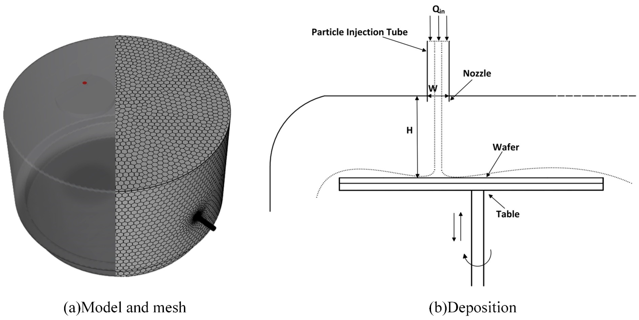
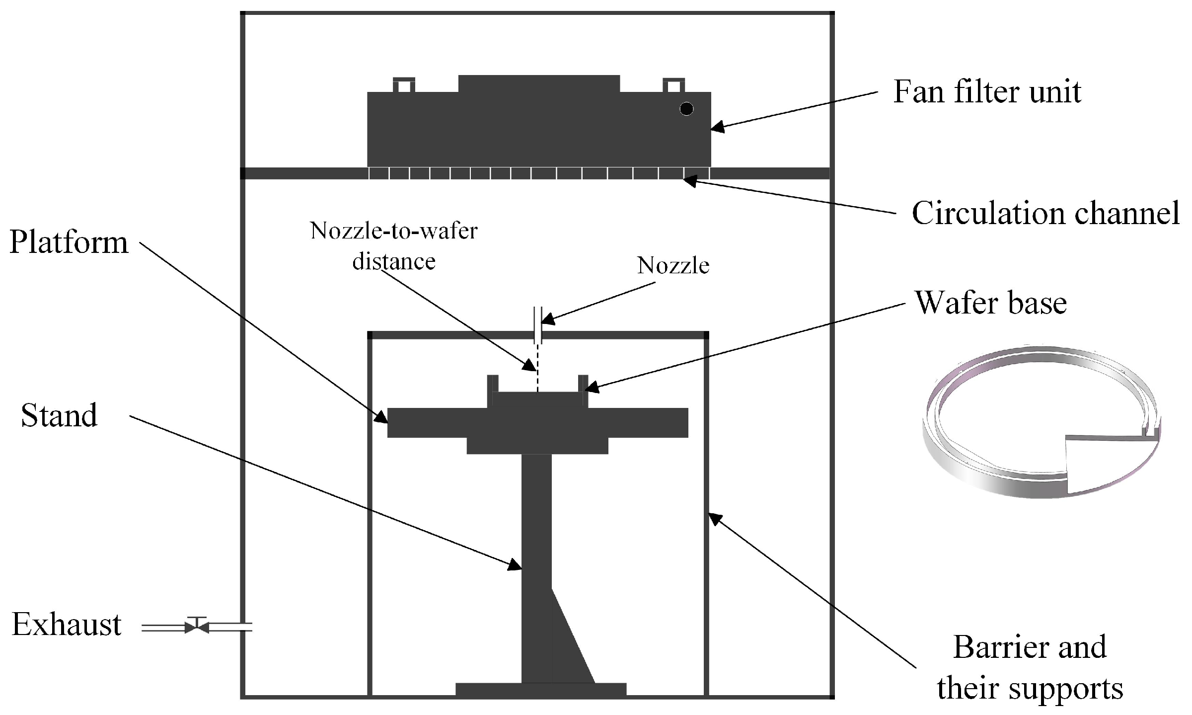
2.1.1. Modeling and Parameters
2.1.2. Solver Settings
- Viscous model: To compute non-uniform, high-curvature rotating flow fields, the realizable k-ε model is employed as the turbulence model. For near-wall treatment, the enhanced wall model is chosen to ensure compatibility with both boundary layer conditions, balancing computational efficiency and accuracy. Additionally, the curvature correction option is enabled to achieve a more accurate simulation of velocity and shear stress distribution.
- Fluid boundary conditions: The inlet is defined as a velocity inlet with a flow velocity of 0.4 m/s, a turbulence intensity of 4%, and a hydrodynamic diameter of 4 mm. The outlet is set as a pressure outlet with a gauge pressure of 100 Pa. All wall surfaces are specified as static, no-slip boundaries with a roughness height of 0 m and a roughness constant of 0.5.
- DPM boundary conditions: The particles are monodisperse, spherical, and inert, with a density of 1050 kg/m3, and their initial velocity at the inlet is synchronized with the airflow (0.4 m/s). The interaction rules between particles and walls are defined as follows: the wafer surface adopts the Trap condition, the inlet and outlet are set as Escape, and all other walls are set as Reflect. The forces acting on the particles include gravity, Saffman force, trailing force, and rotational shear. The discrete random walk (DRW) model is employed to simulate diffusion and vortex effects.
- Numerical solution strategy: The transient pressure-based solver is employed, utilizing the “SIMPLE” algorithm for pressure–velocity coupling with a convergence residual of 10−4. The “PRESTO!” (Pressure Staggering Option) and “Standard” schemes are both interpolation options in ANSYS 2022 Fluent used to calculate pressure values on control volume faces. For pressure term discretization, the “PRESTO!” scheme is applied in rotational cases, while the “Standard” scheme is used for non-rotational cases. The momentum, turbulence, and convection terms are discretized using the “Second-Order Upwind scheme”.
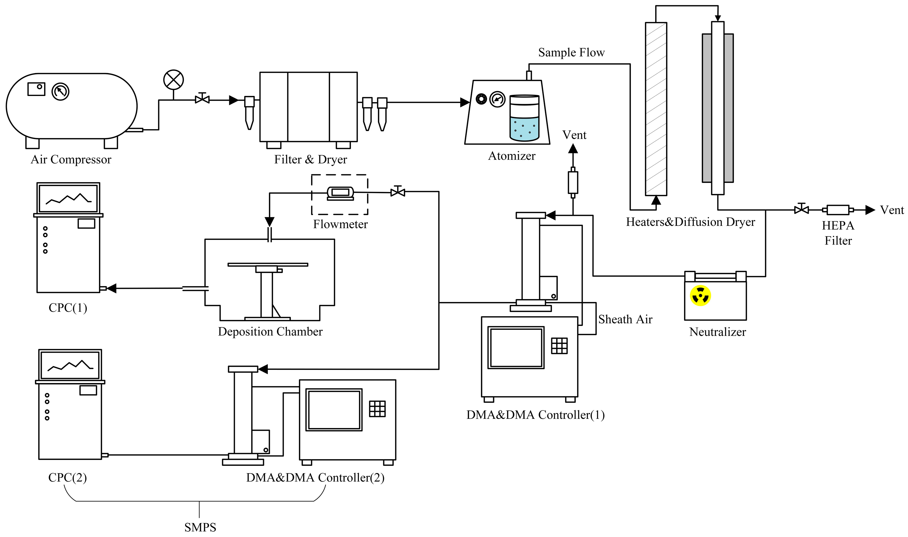
2.2. Experimental Materials and Methods
3. Results and Discussion
3.1. Simulation Results and Analysis
3.1.1. Nozzle Diameter
3.1.2. Nozzle-to-Wafer Distance
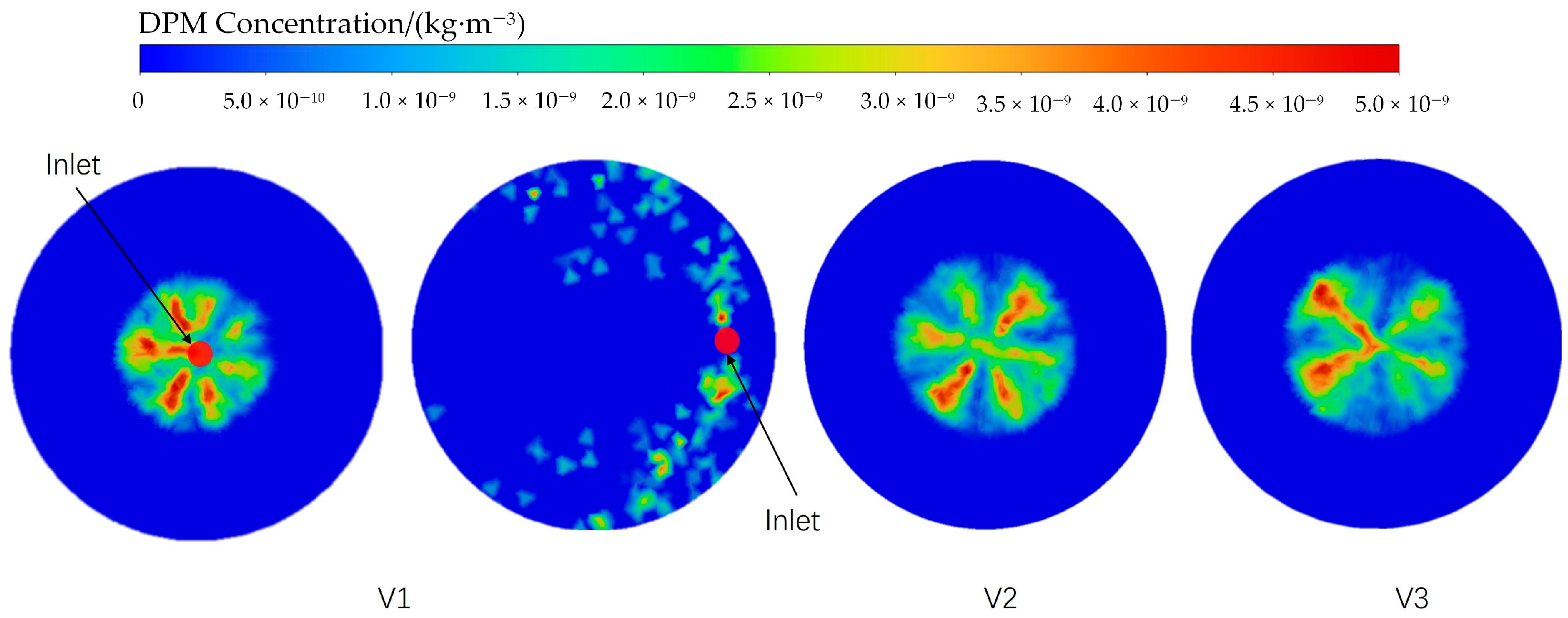
3.1.3. Chamber Volume
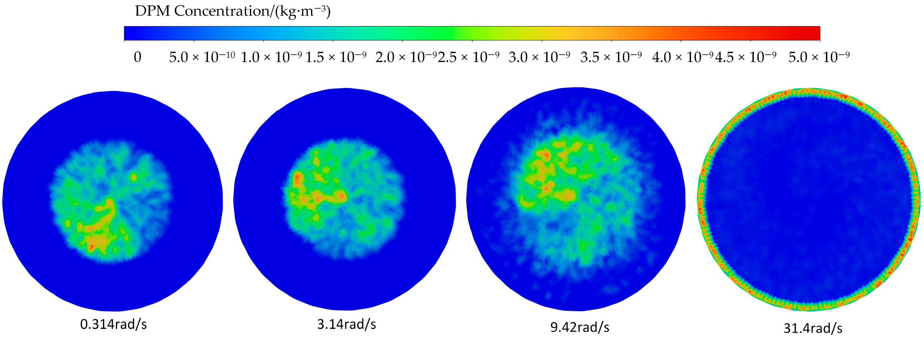
3.1.4. Rotation Speed
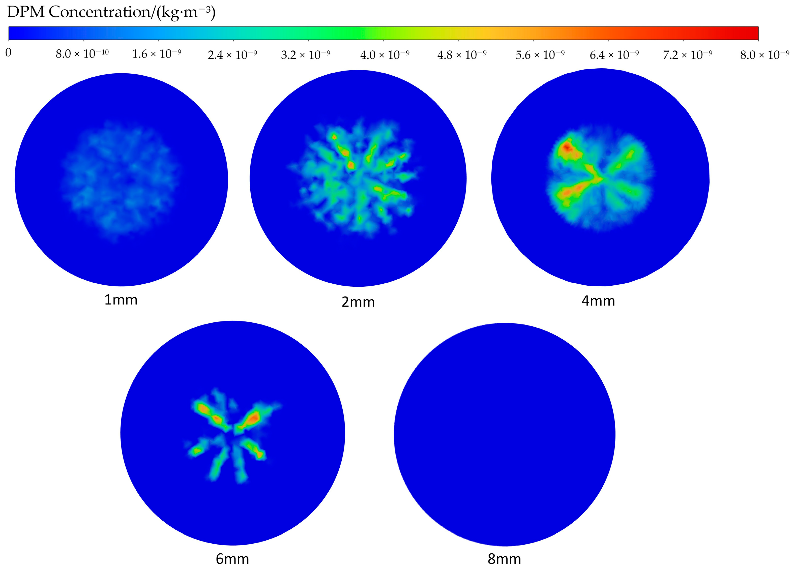
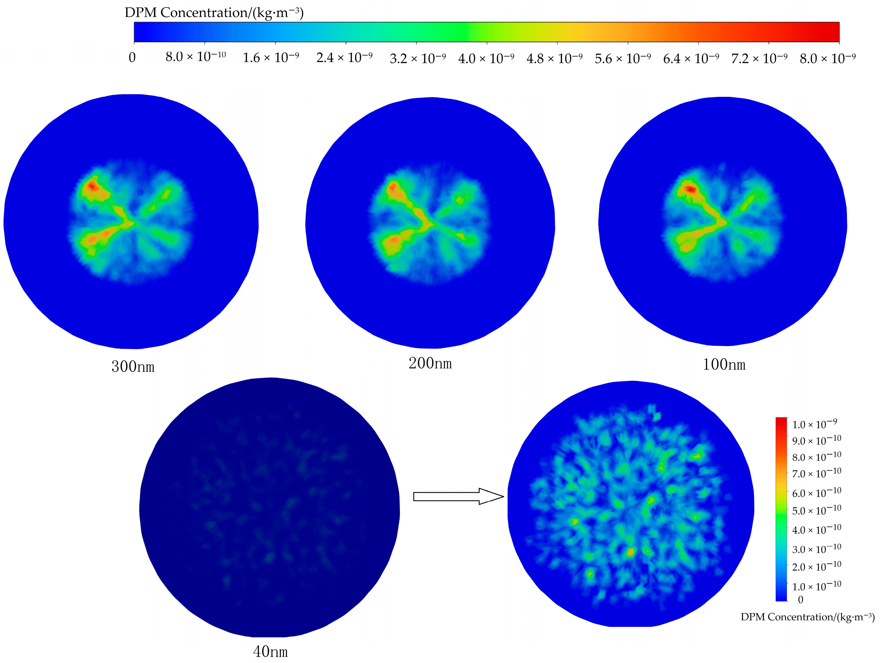
3.1.5. Particle Size
- For smaller particles, diffusion was the dominant deposition mechanism, while inertial effects were insufficient. As a result, fewer particles were deposited directly beneath the nozzle, and most gradually diffused into lower-concentration regions further away.
- Vortices formed by the airflow near the wafer surface significantly influenced smaller particles. The lower the particle mass, the more susceptible it was to turbulence-induced vortex effects, which enhanced particle–surface contact and deposition. Since the experiment considered any particle contacting the wafer as captured, small particles exhibited a broader deposition area.
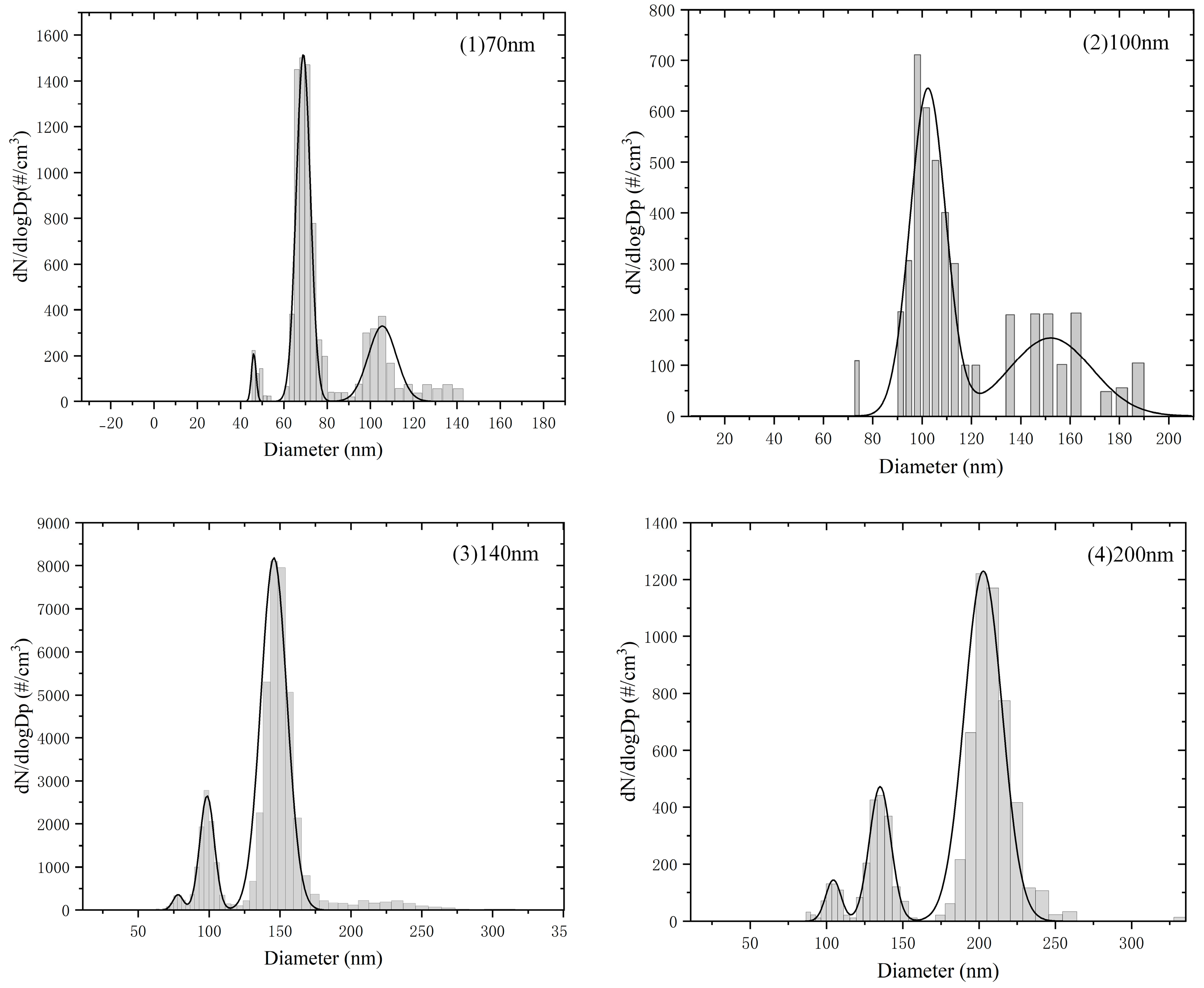
3.2. Aerosol Sample Monodispersity
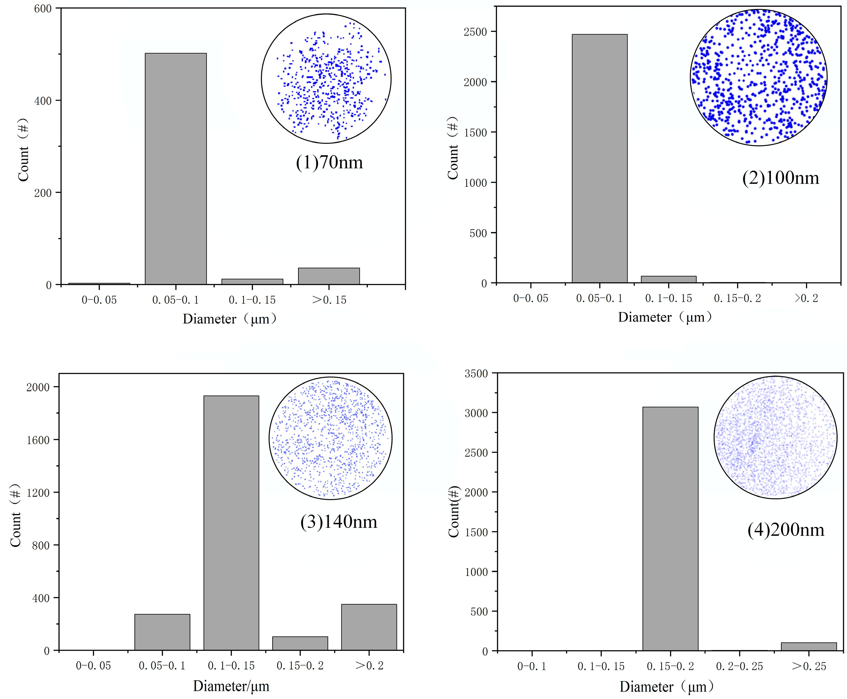
3.3. Standard Wafer Sample
4. Conclusions
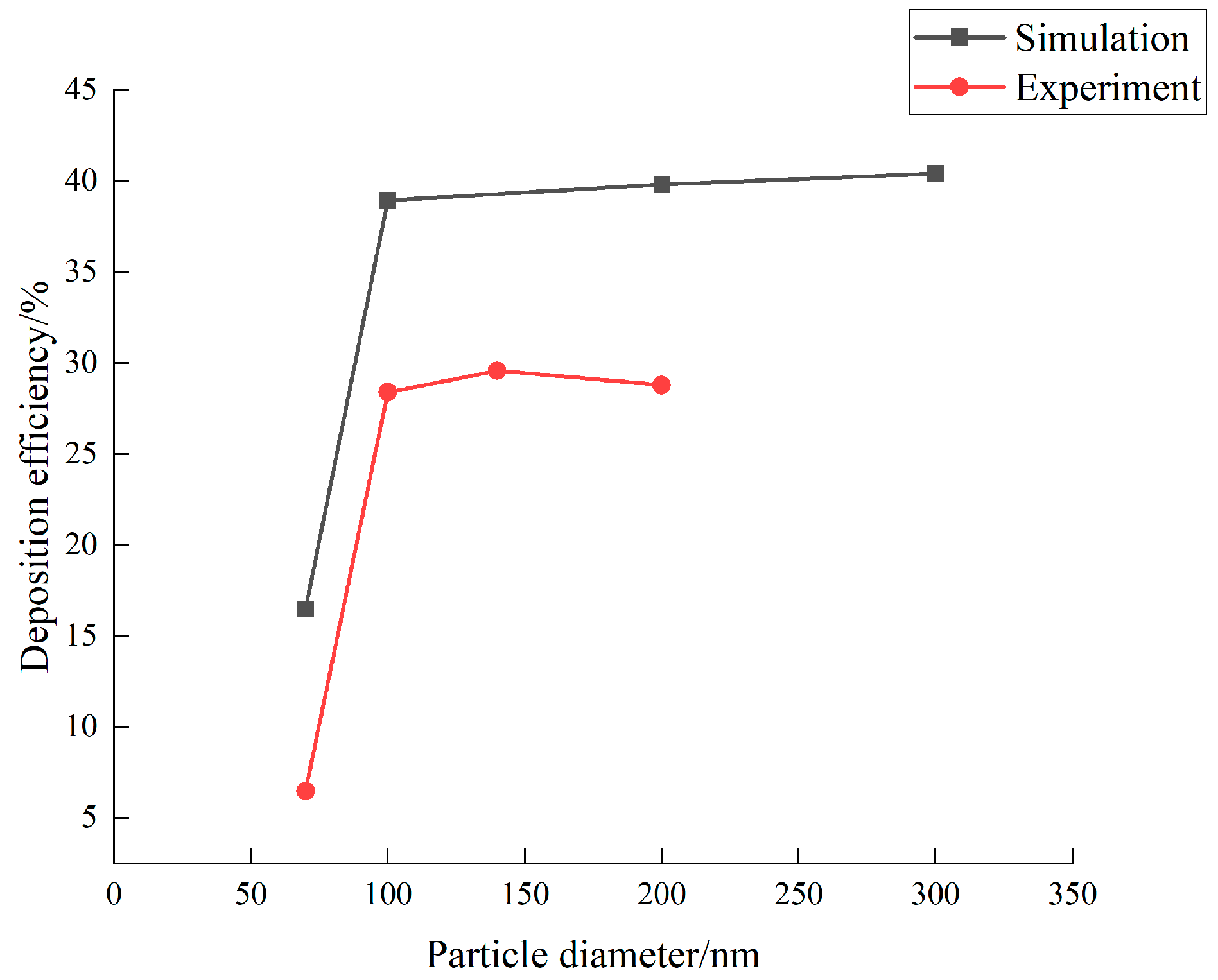
- Fluent simulations identified the optimal parameters for area deposition as a 4 mm nozzle diameter, 15 mm nozzle-to-wafer distance, deposition chamber volume greater than 657 cm3, and a rotation speed of 0.314 rad/s. Under these conditions, uniform deposition can be achieved with a spot diameter of 23.7 mm and a deposition efficiency of 33.1%. Particles ≥100 nm can be stably deposited under standardized parameters, whereas particles <100 nm require adjustments to other parameters to improve deposition efficiency.
- SEM analysis confirmed that the standard PSL suspension used in the experiment aligns with the nominal particle size, making it a suitable raw material for monodisperse aerosol generation. Although multiple particle size peaks were observed in the SMPS scan spectrum, the number concentration at the main peak corresponding to the target particle size was significantly higher than that of the other peaks. Analysis of this phenomenon indicates that SMPS scanning data can serve as a reliable basis for particle size distribution measurement.
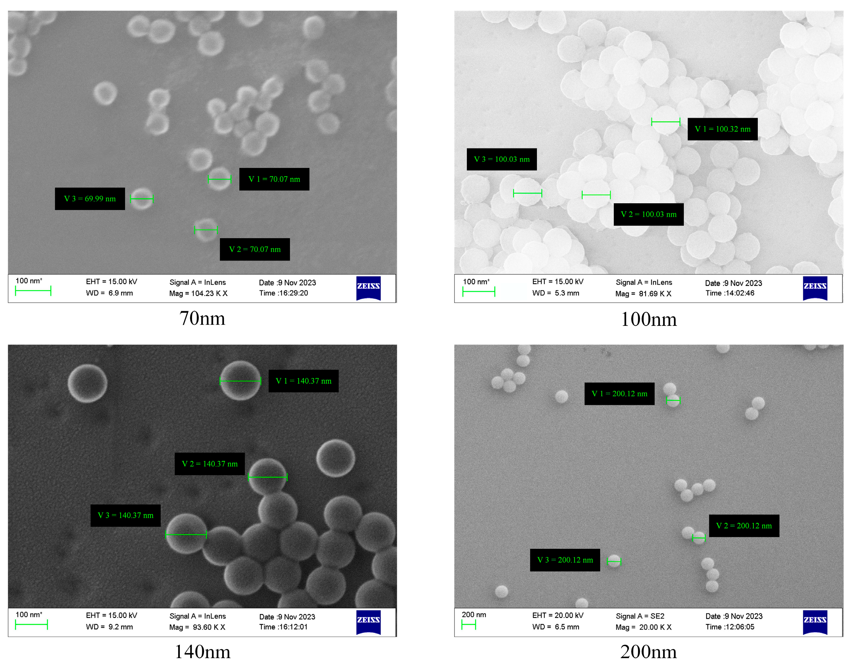
- System validation based on simulation results successfully produced four SW samples (70–200 nm). Experimental results confirmed that the deposition efficiency reached 28% for all samples except the 70 nm sample. SSIS testing further verified that these samples meet the requirements for SSIS calibration.
Author Contributions
Funding
Institutional Review Board Statement
Informed Consent Statement
Data Availability Statement
Acknowledgments
Conflicts of Interest
Abbreviations
| PSL | Polystyrene Latex |
| SSIS | Institute Scanning Surface Inspection System |
| SW | Standard Wafer |
| CFD | Computational Fluid Dynamics |
| SMPS | Scanning Mobility Particle Sizer |
| SEM | Scanning Electron Microscopy |
| CPC | Condenser Particle Counter |
| DMC | Differential Mobility Classifier |
References
- Ma, J.; Zhang, T.; Yang, C.; Cao, Y.; Xie, L.; Tian, H.; Li, X. Review of wafer surface defect detection methods. Electronics 2023, 12, 1787. [Google Scholar] [CrossRef]
- Vines, L.; Monakhov, E.; Kuznetsov, A. Defects in semiconductors. J. Appl. Phys. 2022, 132, 150401. [Google Scholar] [CrossRef]
- Chen, Y.; Ding, Y.; Zhao, F.; Zhang, E.; Wu, Z.; Shao, L. Surface defect detection methods for industrial products: A review. Appl. Sci. 2021, 11, 7657. [Google Scholar] [CrossRef]
- Wang, X.; Jia, X.; Jiang, C.; Jiang, S. A wafer surface defect detection method built on generic object detection network. Digit. Signal Process. 2022, 130, 103718. [Google Scholar] [CrossRef]
- Rasheed, A.; Zafar, B.; Rasheed, A.; Ali, N.; Sajid, M.; Dar, S.H.; Habib, U.; Shehryar, T.; Mahmood, M.T. Fabric defect detection using computer vision techniques: A comprehensive review. Math. Probl. Eng. 2020, 2020, 8189403. [Google Scholar] [CrossRef]
- Zhu, J.; Liu, J.; Xu, T.; Yuan, S.; Zhang, Z.; Jiang, H.; Gu, H.; Zhou, R.; Liu, S. Optical Wafer Defect Inspection at the 10 nm Technology Node and Beyond. Int. J. Extrem. Manuf. 2022, 4, 032001. [Google Scholar] [CrossRef]
- Wu, F.; Cao, P.; Du, Y.; Hu, H.; Yang, Y. Calibration and image reconstruction in a spot scanning detection system for surface defects. Appl. Sci. 2020, 10, 2503. [Google Scholar] [CrossRef]
- Zhou, Z.D. Research on Spot-Scanning Multi-Mode Unpatterned Wafer Defect Inspection Technology and Signal Processing Method. Ph.D. Thesis, University of Science and Technology of China, Hefei, China, 2024. [Google Scholar] [CrossRef]
- Wu, Q.; Zhao, H.; Liu, H. Dynamic visualization study of in situ cleaning of polystyrene microparticles off silicon wafer surface. Phys. Fluids 2024, 36, 113320. [Google Scholar] [CrossRef]
- Lee, S.; Hong, S.; Oh, H.; Chae, S.K.; Kim, T. Study on uniform deposition on 300 mm silicon wafer with sub-100 nm sized particles for cleaning application. Solid State Phenom. 2021, 314, 209–213. [Google Scholar] [CrossRef]
- Kazemimanesh, M.; Rahman, M.M.; Duca, D.; Johnson, T.J.; Addad, A.; Giannopoulos, G.; Focsa, C.; Boies, A.M. A comparative study on effective density, shape factor, and volatile mixing of non-spherical particles using tandem aerodynamic diameter, mobility diameter, and mass measurements. J. Aerosol Sci. 2022, 161, 105930. [Google Scholar] [CrossRef]
- Lee, J.; He, S.; Song, G.; Hogan, C.J. Size distribution monitoring for chemical mechanical polishing slurries: Anintercomparison of electron microscopy, dynamic light scattering, and differential mobility analysis. Powder Technol. 2022, 396, 395–405. [Google Scholar] [CrossRef]
- Yook, S.J.; Fissan, H.; Engelke, T.; Asbach, C.; Van Der Zwaag, T.; Kim, J.H.; Wang, J.; Pui, D.Y.H. Classification of highly monodisperse nanoparticles of NIST-traceable sizes by TDMA and control of deposition spot size on a surface by electrophoresis. J. Aerosol Sci. 2008, 39, 537–548. [Google Scholar] [CrossRef]
- Cho, Y.; Hong, S.; Lee, S.; Yang, J.; Chae, S.-K.; Kim, T. Investigation of a standard particle deposition system on wafer surface and its application to wafer cleaning. ECS J. Solid State Sci. Technol. 2019, 8, 768–774. [Google Scholar] [CrossRef]
- Dick, W.D.; Hegner, L.A.; Li, L. 10 nm particle deposition capability for qualification of next-generation defect inspection tools. In Proceedings of the 2023 34th Annual SEMI Advanced Semiconductor Manufacturing Conference, New York, NY, USA, 1–4 May 2023. [Google Scholar] [CrossRef]
- Lee, S.; Choi, S.; Cho, Y.; Oh, H.; Chae, S.-K.; Kim, T. Uniform deposition method of monodispersed SiO2 nanoparticles on a 300-Mm Si wafer surface. Rev. Sci. Instrum. 2021, 92, 113704. [Google Scholar] [CrossRef] [PubMed]
- Tajima, N.; Iida, K.; Ehara, K.; Khumpuang, S.; Hara, S.; Sakurai, H. A method to deposit a known number of polystyrene latex particles on a flat surface. Aerosol Sci. Technol. 2019, 53, 1353–1366. [Google Scholar] [CrossRef]
- Matsuno, K.; Mishima, H.; Arimatsu, M.; Kikuchi, S.; Shikami, S. The wafer preparation technology with nano size particle contamination by using single spin processor. In Proceedings of the 2006 IEEE International Symposium on Semiconductor Manufacturing, Tokyo, Japan, 25–27 September 2006. [Google Scholar] [CrossRef]
- Li, S.; Ali, K.; Algarni, S.; Alqahtani, T.; Ahmad, S.; ElSeabee, F.A.A.; Ullah, H.; Jamshed, W.; Irshad, K. Numerical analysis of thermophoretic particle deposition in a Magneto-Marangoni convective dusty tangent hyperbolic nanofluid Flow—Thermal and Magnetic features. Nanotechnol. Rev. 2024, 13, 20230190. [Google Scholar] [CrossRef]
- Abbas, M.; Khan, N.; Hashmi, M.S.; Alhefthi, R.K.; Inc, M. Significance of heat generation and thermophoretic particle deposition in Marangoni convective driven boundary layer flow of cross nanofluid with activation energy. Case Stud. Therm. Eng. 2024, 59, 104427. [Google Scholar] [CrossRef]
- Bae, G.N.; Lee, C.S.; Park, S.O. Measurement of Particle Deposition Velocity Toward a Horizontal Semiconductor Wafer by Using a Wafer Surface Scanner. Aerosol Sci. Technol. 1994, 21, 72–82. [Google Scholar] [CrossRef]
- Flagan, R.C. History of electrical aerosol measurements. Aerosol Sci. Technol. 1998, 28, 301–380. [Google Scholar] [CrossRef]


| Aerosol Flow Rate = 0.3 L/min | |||||
|---|---|---|---|---|---|
| Dp/nm | Dnoozle/mm | H/mm | V/cm3 | N/rad·s−1 | |
| Dnozzle | 300 | 1, 2, 4, 6, 8 | 15 | 3650 | 0 |
| H | 300 | 4 | 5, 15, 50 | 3650 | 0 |
| V | 300 | 4 | 15 | 81, 657, 3650 | 0 |
| N | 300 | 4 | 15 | 3650 | 0.314, 3.14, 31.4 |
| Dp | 70, 100, 200, 300 | 4 | 15 | 3650 | 0 |
| Materials and Instrumentation | Parameters and Models | Manufacturer | Sourced |
|---|---|---|---|
| PSL standard suspension | 70–200 nm | National Institute of Metrology, China | Beijing, China |
| Clean wafers | 50 mm | Topvendor | Beijing, China |
| Atomization generator | ATM 220 | Topas GmbH | Dresden, Germany |
| Cold dryer | HLW-10 AC | Hailvwang | Hangzhou, China |
| Neutralizer | 5.520 | Grimm | Ainring, Germany |
| Differential mobility classifier | 55-U | Grimm | Ainring, Germany |
| Condenser particle counter | 3775 | TSI Inc. | Shoreview, MN, USA |
| Scanning mobility particle sizer | S 82 | TSI Inc. | Shoreview, MN, USA |
| Scanning surface inspection system | E3200 | AK OPTICS | Beijing, China |
| Scanning electron microscope | Ultra 55 | ZEISS | Oberkochen, Germany |
| Particle Size/nm | Number of Deposited Particles/# | Deposition Efficiency/% |
|---|---|---|
| 70 | 502 | 6.5% |
| 100 | 2470 | 27.4% |
| 140 | 2031 | 29.6% |
| 200 | 3069 | 28.4% |
Disclaimer/Publisher’s Note: The statements, opinions and data contained in all publications are solely those of the individual author(s) and contributor(s) and not of MDPI and/or the editor(s). MDPI and/or the editor(s) disclaim responsibility for any injury to people or property resulting from any ideas, methods, instructions or products referred to in the content. |
© 2025 by the authors. Licensee MDPI, Basel, Switzerland. This article is an open access article distributed under the terms and conditions of the Creative Commons Attribution (CC BY) license (https://creativecommons.org/licenses/by/4.0/).
Share and Cite
Zhang, Z.; Ren, J.; Liu, Y.; Liu, J. Numerical Simulation-Based Study of Controlled Particle Deposition Technology for Wafer Surfaces. Appl. Sci. 2025, 15, 6970. https://doi.org/10.3390/app15136970
Zhang Z, Ren J, Liu Y, Liu J. Numerical Simulation-Based Study of Controlled Particle Deposition Technology for Wafer Surfaces. Applied Sciences. 2025; 15(13):6970. https://doi.org/10.3390/app15136970
Chicago/Turabian StyleZhang, Ziheng, Jun Ren, Yue Liu, and Junjie Liu. 2025. "Numerical Simulation-Based Study of Controlled Particle Deposition Technology for Wafer Surfaces" Applied Sciences 15, no. 13: 6970. https://doi.org/10.3390/app15136970
APA StyleZhang, Z., Ren, J., Liu, Y., & Liu, J. (2025). Numerical Simulation-Based Study of Controlled Particle Deposition Technology for Wafer Surfaces. Applied Sciences, 15(13), 6970. https://doi.org/10.3390/app15136970