
Surface Charging on Insulating Films with Different Thicknesses in UPS

Abstract
1. Introduction
2. Materials and Methods
3. Results and Discussion
3.1. Time-Dependent Residual Thickness
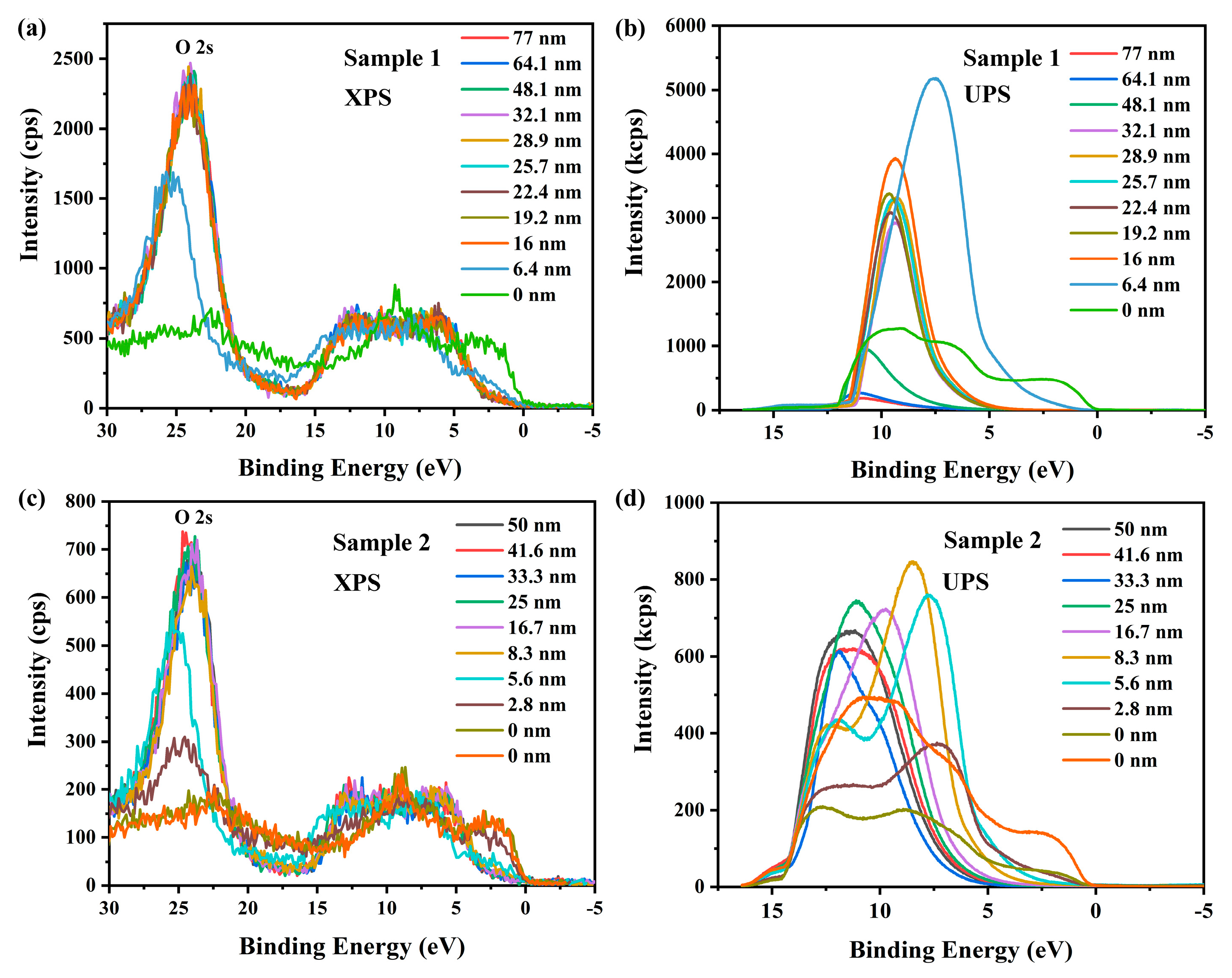
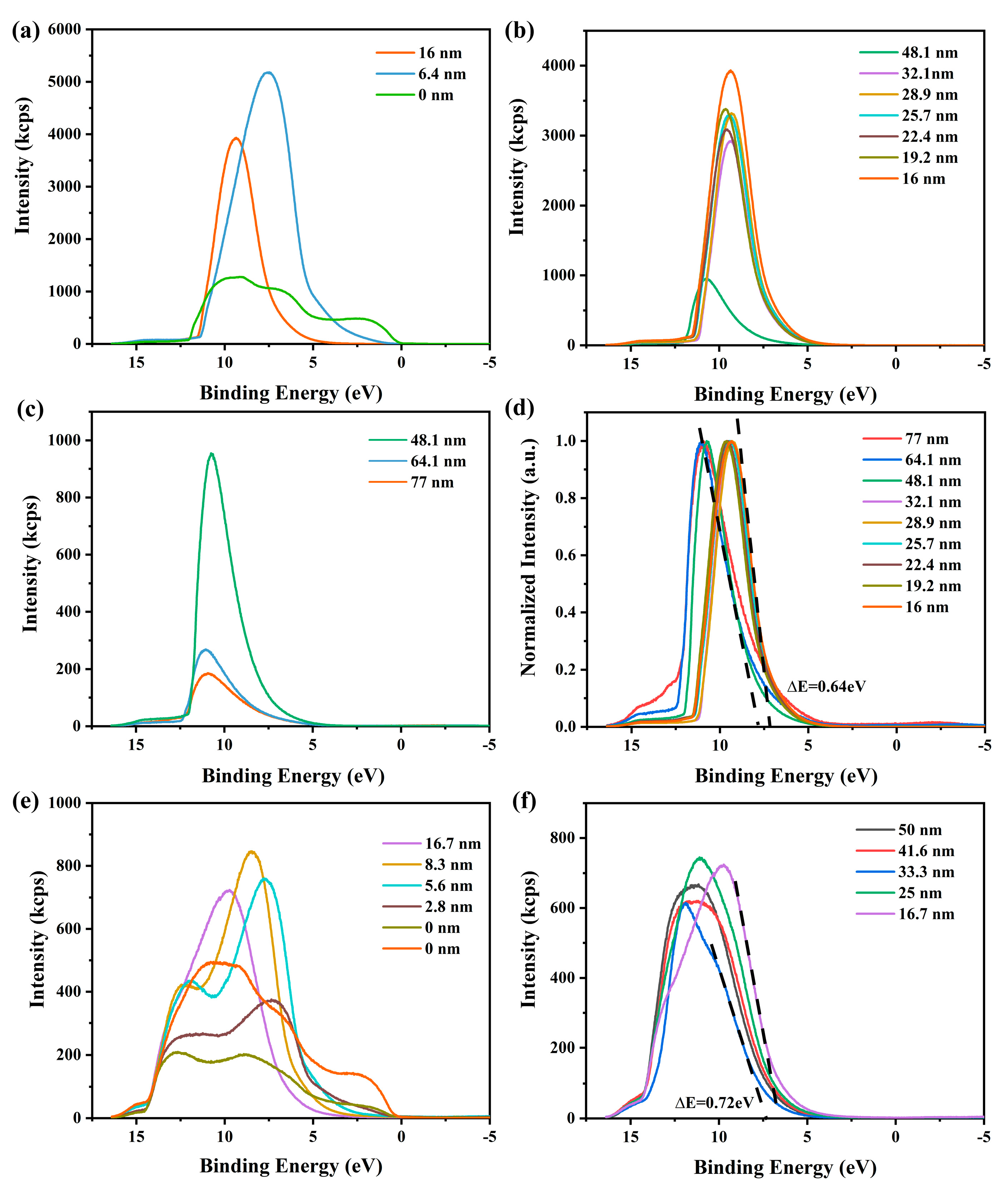
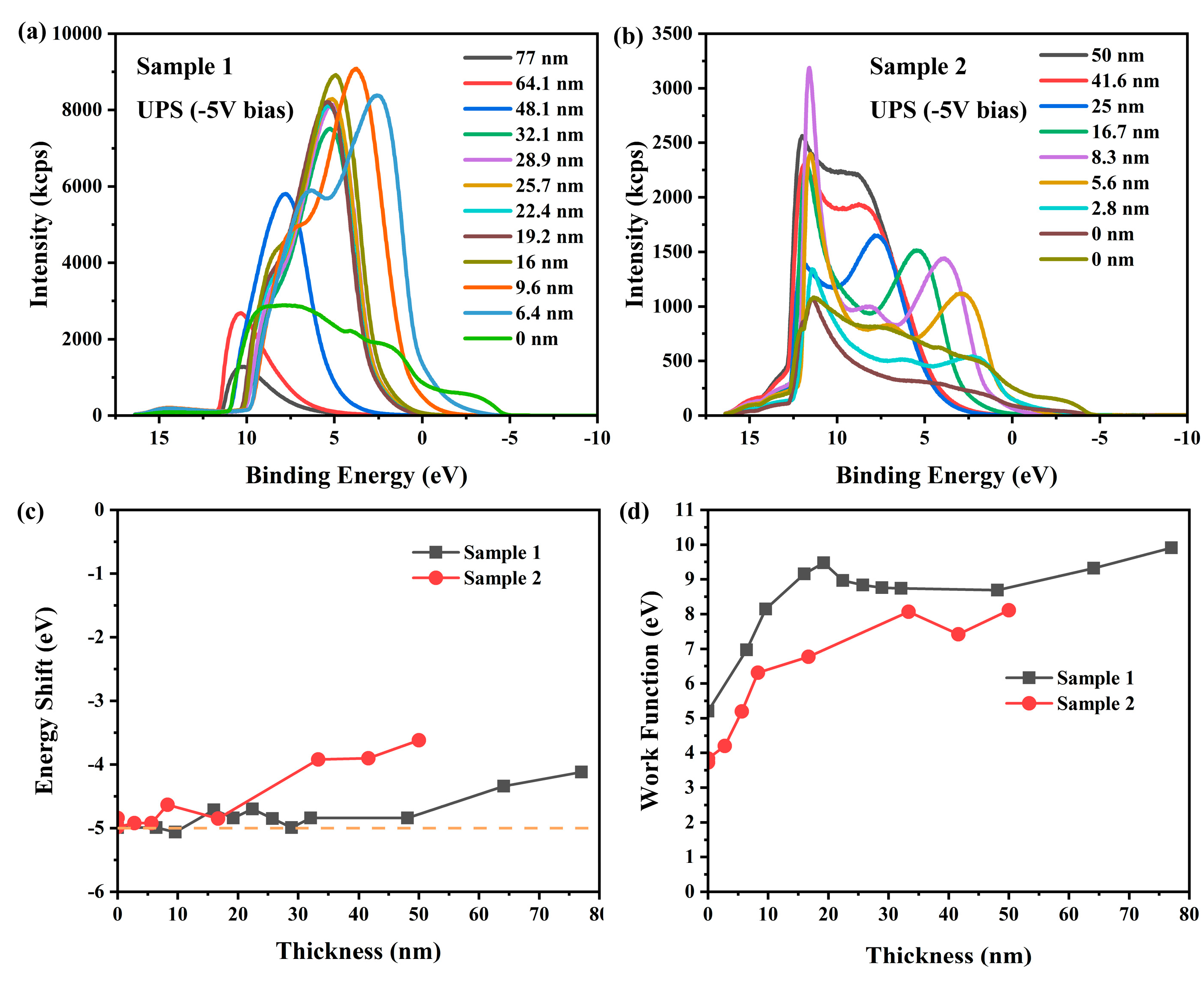
3.2. Observations of Photoelectron Spectra
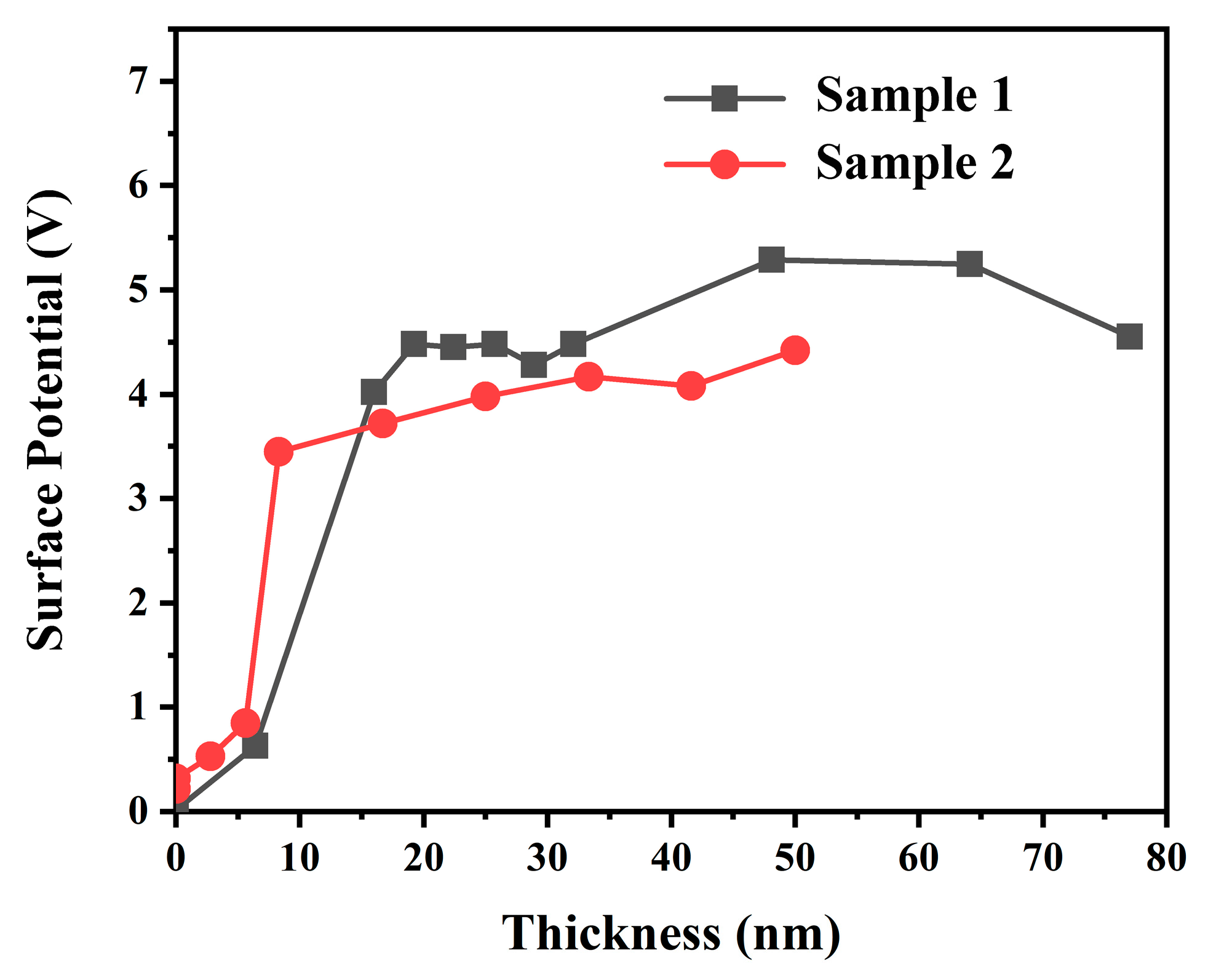
3.3. Charging-Induced Surface Potential
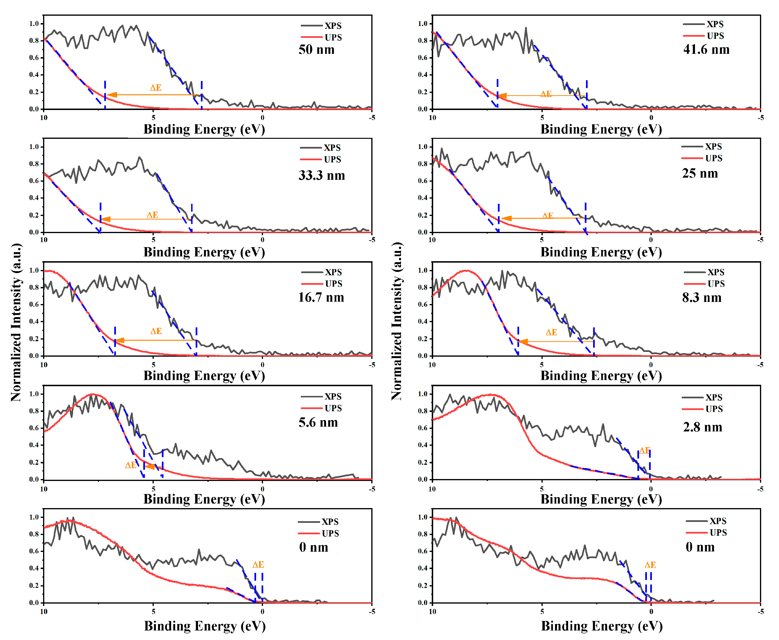
3.4. Work Function Analysis
4. Conclusions
Author Contributions
Funding
Institutional Review Board Statement
Informed Consent Statement
Data Availability Statement
Conflicts of Interest
Abbreviations
| UPS | Ultraviolet photoelectron spectroscopy |
| XPS | X-ray photoelectron spectroscopy |
| BE | Binding energy |
| VBM | Valence band maximum |
| WF | Work function |
References
- Whitten, J.E. Ultraviolet photoelectron spectroscopy: Practical aspects and best practices. Appl. Surf. Sci. Adv. 2023, 13, 100384. [Google Scholar] [CrossRef]
- Shao, G. Work function and electron affinity of semiconductors: Doping effect and complication due to fermi level pinning. Energy Environ. Mater. 2021, 4, 273–276. [Google Scholar] [CrossRef]
- Wang, S.; Sakurai, T.; Wen, W.; Qi, Y. Energy level alignment at interfaces in metal halide perovskite solar cells. Adv. Mater. Interfaces 2018, 5, 1800260. [Google Scholar] [CrossRef]
- Cazaux, J. Mechanisms of charging in electron spectroscopy. J. Electron Spectrosc. Relat. Phenom. 1999, 105, 155–185. [Google Scholar] [CrossRef]
- Cazaux, J. Electromigration and charging effects during auger and xps analysis of insulators. Surf. Interface Anal. 1986, 9, 133–134. [Google Scholar] [CrossRef]
- Edwards, L.; Mack, P.; Morgan, D.J. Recent advances in dual mode charge compensation for XPS analysis. Surf. Interface Anal. 2019, 51, 925–933. [Google Scholar] [CrossRef]
- Salaneck, W.R. Classical ultraviolet photoelectron spectroscopy of polymers. J. Electron Spectrosc. Relat. Phenom. 2009, 174, 3–9. [Google Scholar] [CrossRef]
- Baer, D.R.; Artyushkova, K.; Cohen, H.; Easton, C.D.; Engelhard, M.; Gengenbach, T.R.; Greczynski, G.; Mack, P.; Morgan, D.J.; Roberts, A. XPS guide: Charge neutralization and binding energy referencing for insulating samples. J. Vac. Sci. Technol. A 2020, 38, 031204. [Google Scholar] [CrossRef]
- Greczynski, G.; Hultman, L. X-ray photoelectron spectroscopy: Towards reliable binding energy referencing. Prog. Mater. Sci. 2020, 107, 100591. [Google Scholar] [CrossRef]
- Leisenberger, F.; Duschek, R.; Czaputa, R.; Netzer, F.P.; Beamson, G.; Matthew, J. A high resolution XPS study of a complex insulator: The case of porous silicon. Appl. Surf. Sci. 1997, 108, 273–281. [Google Scholar] [CrossRef]
- Sherwood, P. Charging Issues in Electron Spectroscopies Preface; Elsevier Science: Amsterdam, The Netherlands, 2010; Volume 176, pp. 2–4. [Google Scholar]
- Tielsch, B.J.; Fulghum, J.E. Differential charging in XPS. Part III. A comparison of charging in thin polymer overlayers on conducting and non-conducting substrates. Surf. Interface Anal. 1997, 25, 904–912. [Google Scholar] [CrossRef]
- Bergman, S.L.; Sahasrabudhe, G.S.; Ji, H.; Cava, R.J.; Bernasek, S.L. Useful X-ray photoelectron spectroscopy-based chemical tool: Differential charging studies of complex composite materials. Chem. Mater. 2017, 29, 4162–4166. [Google Scholar] [CrossRef]
- Metson, J.B. Charge compensation and binding energy referencing in XPS analysis. Surf. Interface Anal. 1999, 27, 1069–1072. [Google Scholar] [CrossRef]
- Mukherjee, S.; Mukherjee, M. Controlled surface neutralization: A quantitative approach to study surface charging in photoemission. J. Electron Spectrosc. Relat. Phenom. 2007, 154, 90–95. [Google Scholar] [CrossRef]
- Mori, Y. Practical Technique for Restraining Differential Charging in X-ray Photoelectron Spectros copy: Os Coating. J. Surf. Anal. 2005, 12, 113. [Google Scholar]
- Astm, E. Standard Guide to Charge Control and Charge Referencing Techniques in X-Ray Photoelectron Spectroscopy; ASTM International: West Conshohocken, PA, USA, 2015. [Google Scholar]
- Zhu, L.; Li, W.; Ma, L.; Xu, X.; Luo, J. Observations on Valence-Band Electronic Structure and Surface States of Bulk Insulators Based on Fast Stabilization Process of Sample Charging in UPS. Laser Photonics Rev. 2024, 18, 2301069. [Google Scholar] [CrossRef]
- Salaneck, W.R. Conjugated polymer surfaces and interfaces. Philos. Trans. R. Soc. Lond. Ser. A Math. Phys. Eng. Sci. 1997, 355, 789–799. [Google Scholar] [CrossRef]
- Filatova, E.O.; Konashuk, A.S. Interpretation of the Changing the Band Gap of Al2O3 Depending on Its Crystalline Form: Connection with Different Local Symmetries. J. Phys. Chem. C 2015, 119, 20755–20761. [Google Scholar] [CrossRef]
- Lewandków, R.; Grodzicki, M.; Mazur, P.; Ciszewski, A. Interface formation of Al2O3 on carbon enriched 6H-SiC(0001): Photoelectron spectroscopy studies. Vacuum 2020, 177, 109345. [Google Scholar] [CrossRef]
- Kang, J.; Lee, J.H.; Lee, H.; Kim, K.; Kim, J.H.; Maeng, M.; Hong, J.; Park, Y.; Kim, K.H. Effect of threading dislocations on the electronic structure of La-doped BaSnO3 thin films. Materials 2022, 15, 2417. [Google Scholar] [CrossRef]
- Gutierrez, G.; Guessous, H.; Gosset, D.; Bricout, M.; Monnet, I.; Garrido, F.; Onofri, C.; Adroit, G.; Debelle, A. Defect evolution under intense electronic energy deposition in uranium dioxide. J. Nucl. Mater. 2023, 578, 154375. [Google Scholar] [CrossRef]
- Hollinger, G. Structures chimique et electronique de l’interface SiO2-Si. Appl. Surf. Sci. 1981, 8, 318–336. [Google Scholar] [CrossRef]
- Chastain, J.; King, R.C., Jr. Handbook of X-Ray Photoelectron Spectroscopy; Perkin-Elmer Corporation: Waltham, MA, USA, 1992; Volume 40, p. 25. [Google Scholar]
- Ozawa, Y.; Nakayama, Y.; Machida, S.I.; Kinjo, H.; Ishii, H. Maximum probing depth of low-energy photoelectrons in an amorphous organic semiconductor film. J. Electron Spectrosc. Relat. Phenom. 2014, 197, 17–21. [Google Scholar] [CrossRef]
- Kim, E.; Hwang, G.; Kim, D.; Won, D.; Joo, Y.; Zheng, S.; Watanabe, K.; Taniguchi, T.; Moon, P.; Kim, D.W. Orbital gating driven by giant Stark effect in tunneling phototransistors. Adv. Mater. 2022, 34, 2106625. [Google Scholar] [CrossRef] [PubMed]

Disclaimer/Publisher’s Note: The statements, opinions and data contained in all publications are solely those of the individual author(s) and contributor(s) and not of MDPI and/or the editor(s). MDPI and/or the editor(s) disclaim responsibility for any injury to people or property resulting from any ideas, methods, instructions or products referred to in the content. |
© 2025 by the authors. Licensee MDPI, Basel, Switzerland. This article is an open access article distributed under the terms and conditions of the Creative Commons Attribution (CC BY) license (https://creativecommons.org/licenses/by/4.0/).
Share and Cite
Zhu, L.; Xu, X. Surface Charging on Insulating Films with Different Thicknesses in UPS. Appl. Sci. 2025, 15, 6846. https://doi.org/10.3390/app15126846
Zhu L, Xu X. Surface Charging on Insulating Films with Different Thicknesses in UPS. Applied Sciences. 2025; 15(12):6846. https://doi.org/10.3390/app15126846
Chicago/Turabian StyleZhu, Lei, and Xuefeng Xu. 2025. "Surface Charging on Insulating Films with Different Thicknesses in UPS" Applied Sciences 15, no. 12: 6846. https://doi.org/10.3390/app15126846
APA StyleZhu, L., & Xu, X. (2025). Surface Charging on Insulating Films with Different Thicknesses in UPS. Applied Sciences, 15(12), 6846. https://doi.org/10.3390/app15126846