1. Introduction
The growing complexity of digital systems and the rising demands for their flexibility (ease of reconfiguration) mean that programmable logic circuits are playing an ever more important role. The leading devices in this group are FPGAs (Field Programmable Gate Arrays). Their considerable logic resources allow the easy implementation of complex digital systems at relatively low cost. The short prototyping time for circuit solutions cannot be underestimated either.
A number of advantages of FPGA devices have made them widely used in industries where fast signal processing is required. It appears that FPGAs are also applied in areas such as medicine, the military, nuclear power, and space industries, where they perform critical functions [
1,
2]. In each of these areas, the reliability of the implemented system is crucial; oftentimes, as in military or space applications, mobility is also vital. Mobility in this context is understood as maximizing battery life, which is directly related to the energy efficiency of the implemented systems. Of course, reliability and energy efficiency are interrelated (reducing the amount of heat emitted by a device, especially thermal stress, reduces the probability of failure).
In the applications mentioned earlier, one of the main sources of failure or malfunction is the effect of ionizing radiation. Especially in the area of space applications, the problem of radiation effects on FPGAs is extremely important [
3]. Radiation affects semiconductor devices in two ways: Single Event Effects (SEEs) and dose effects. Dose effects correspond to a permanent change in selected parameters as a result of prolonged radiation exposure (prolonged exposure to ionizing radiation causes degradation of the crystal lattice, which affects the resistivity of the semiconductor; it is also possible that the material itself begins to accumulate a positive electrical charge), while SEEs are related to phenomena resulting from the effect of a particle on a logic structure and can cause a change in the value of individual bits [
4]. Mitigation techniques include appropriate manufacturing processes at the physical level [
5,
6] or appropriate digital circuit design (FPGA implementation) [
3,
7,
8]. The primary mitigation method for configuration memory is scrubbing—memory is ‘refreshed’ from an external source [
9,
10,
11,
12]. Dynamic and partial reconfiguration can help to detect, isolate, and recover from SEU faults [
13]. In case of implemented design, there are also mitigation techniques like Error Checking and Correction (ECC) [
14], which most commonly uses the Hamming code [
15] or the Reed–Solomon code [
16]. Sometimes, elements of FPGAs are used for special purpose—BlockRAM as a sensor [
17].
Redundancy is a basic, albeit costly, technique for increasing the probability of correct system operation. It involves for example duplicating selected blocks several times in order to perform exactly the same task. If the duplicated modules operate in exactly the same way at the same time (the state of their outputs is the same), this means that no SEE-induced errors have occurred in the operation of the modules. However, if the signals on their outputs are different, this means that an error must have occurred in one of the duplicated modules. Triple modular redundancy (TMR) is commonly used in practice—three identical and independent modules perform the same function. The outputs of these modules are attached to the majority voting circuit, so that the state of the module outputs can be uniquely determined during the voting process (a single fault is assumed). TMR is the subject of a number of scientific papers [
18,
19,
20,
21,
22]. Fault-tolerant systems without redundancy are also designed [
23].
Naturally, the use of TMR results in a significant increase in the number of logical resources used, and thus, in power dissipation. Design constraints imposed by, for example, the availability of FPGA logic resources or performance expectations are driving the development of ever-newer logic synthesis methods: [
24,
25,
26] or [
27,
28]. Appropriate logic synthesis methods are, therefore, required [
29,
30,
31,
32,
33]. In the paper [
34], a software–hardware co-design approach for the development of a power-efficient real-time traffic signal classification system tailored for FPGAs utilizing the convolutional neural network algorithm is proposed. Low-power strategies toward FPGA-based wearable medical device for physiological monitoring are described in [
35]. Techniques like Clock Enable (CE) inputs utilization [
36] or specific register–transfer level code generation [
37] may be used to design low-power modules. Naturally, the key from the perspective of a low-power minimization-oriented synthesis strategy is what type of circuits will be synthesized. In general, combinatorial and sequential circuits can be distinguished in digital technology. In the case of combinatorial circuits, the aim is generally to reduce switching activity [
30,
31]. In the case of sequential circuits, on the other hand, power reductions can be achieved by appropriate encoding of internal states [
33].
Sequential circuits are the dominant group in digital technology. An important group here is the finite state machine (FSM). The question arises as to how TMR-based mitigation can most effectively be fitted into the FSM. There is also the question of which blocks in the FSM should be triplicated and where TMR-based voters should be included in the FSM structure.
The main objective of this paper is to present the different possibilities of applying triple modular redundancy in finite state machines. Experiments with different benchmarks have been realized. The different structures have been synthesized and compared in terms of logic utilization, number of logic levels, and power dissipation. Error-correction efficiency and recovery capability have also been analyzed. This article is an extension of the authors’ earlier article on voting circuits [
38], towards triple modular redundancy for sequential circuits.
The article is divided into sections.
Section 2 contains a description of the FSMs and the essence of the TMR.
Section 3 presents the authors’ proposed models for the implementation of TMR in the FSM structure and is followed by a summary in (
Section 4).
Section 5 presents the results of the experiments obtained with both academic and commercial tools. The article ends with some conclusions in
Section 6.
2. Theoretical Background
In this section, definitions and concepts related to FSMs will be presented. Later, the basics of triple modular redundancy will be presented and sources of radiation errors described.
2.1. Finite State Machine
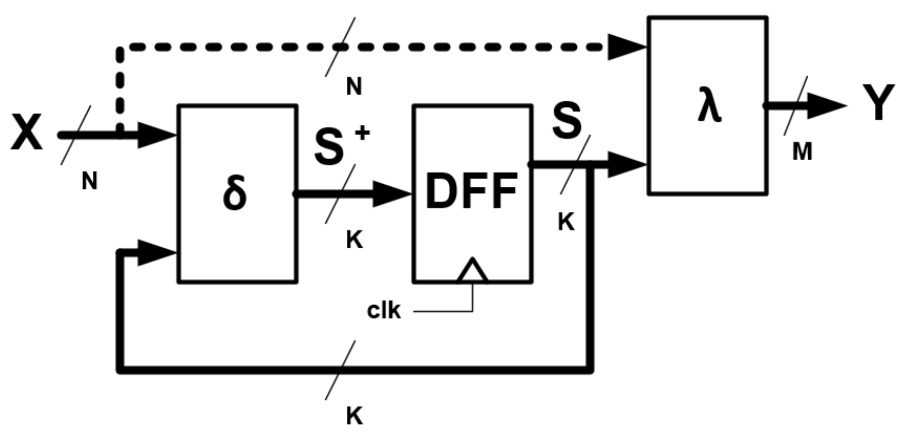
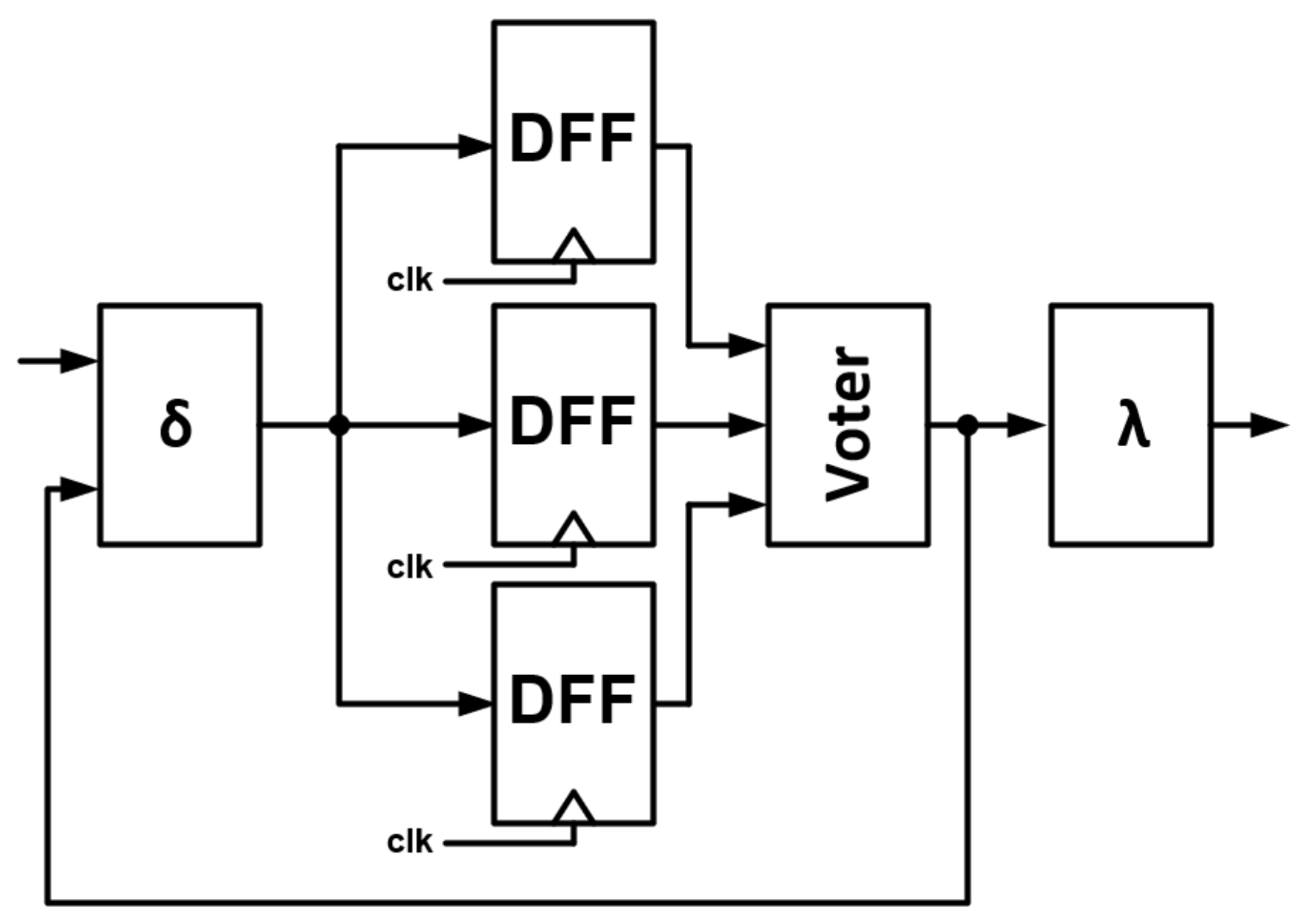
The FSM represents a model of a sequential digital circuit in which the operation (its output vector) depends on both the values at the inputs of the circuit and the internal state of the circuit. Naturally, the internal state must be stored in some block of memory. In addition, the FSM contains a combinatorial part, which makes these circuits more complex than simple combinatorial circuits.
A finite state machine is a mathematical model of computation. The FSM can be described using five elements:
, where
X is the set of input elements,
Y is the set of output elements, and
S is the set of the internal states. The last two elements describe the relationship between the other elements, where
is the transition function and
is the output function. The general structure of the FSM is shown in
Figure 1.
The key element of the structure in
Figure 1 is the memory block labeled DFF, and is most often implemented in the circuit as a parallel register (called state register). It stores a
K-bit current state vector
S, where
. The value of the next state
is determined by the transition function
:
. The arguments of this function are the current state vector
S and the
N-bit input vector
X, where
. Naturally, the transition function is realized by a combinatorial block
:
, where
. The output value
Y, which is an
M-bit vector, where
is determined by the output function
. The output function can take two forms:
In the case of Moore’s FSM, the function of the outputs depends only on the current state of S. In the case of Mealy’s FSM, the output function depends additionally on the state of the X inputs. The output function is a combinatorial block which can be represented as:
Both the transition function and the output function are implemented in blocks marked with the same symbols (hereafter, transition block and output block).
Naturally, from the point of view of mitigating radiation effects in FSM circuits, the introduction of TMR is crucial.
2.2. Radiation-Induced Error Types
One of the errors from the entire SEE set is the Single Event Upset (SEU), which corresponds to a change in the state of a memory element as a result of the impact of a high-energy particle. In FPGAs, these changes can be at two different levels: in the memory elements of the implementation and in the memory elements of the configuration memory. The impact types with their causes and effects are summarized in
Table 1. This article focuses on the impact type SEE, which results in an SEU.
Single Event Effects are caused by a single, energetic particle such as protons, neutrons, or heavy ions, and can take on many forms [
3,
39], i.e., if an ion particle transversing a device deposits sufficient charge, an event such as a memory bit flip or transient may occur, which may be destructive or not. The destructive (like Single-Event Latch-up (SEL), Single-Event Gate Rupture (SEGR), or Single-Event Burnout (SEB)) are not considered in this paper.
The non-destructive errors are described as soft errors. The SEUs are characterized by a single particle strike in memory elements leading to bit flips and consequently data corruption. The downsizing of transistors, associated with smaller supply voltages and higher operating frequencies, has resulted in Single Event Transients (SETs) and is referred to combinatorial logic [
40].
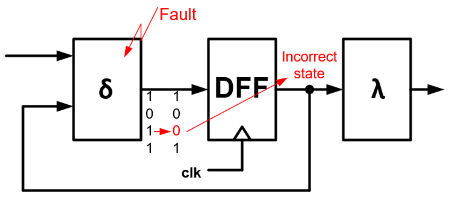
Considering the FSM, both SET and SEU can have a significant impact on the performance of the FSM. A change of state in a state register DFF cell can result in an incorrect determination in the transition block the excitation for the state register DFF. Of course, the output block can also give an incorrect logic state in response.
The SET in the transition block can have a similar effect. A change of logic state in a combinatorial circuit can cause the state register DFF to latch into a bad state or a metastability phenomenon to occur.
If SET occurs in the output block , the FSM response may be incorrect.
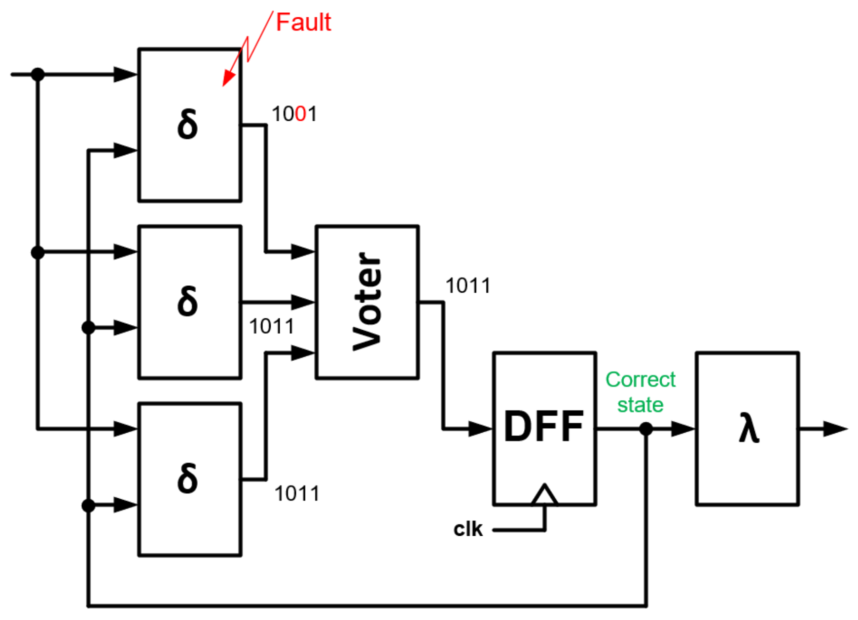
The impact of SET on internal FSM state is presented in
Figure 2. As an effect, the transition block
outputs with 1001 state instead of 1011. If an error is latched in the state register DFF, the FSM will be in a different state than it should be, potentially disrupting the whole system.
2.3. Triple Modular Redundancy
The essence of TMR is to triplicate selected modules and compare the states of their outputs. By majority voting, the correct answer from the triplicated modules is determined. This leads to the conclusion that the voting circuit (the voter) is a key element.
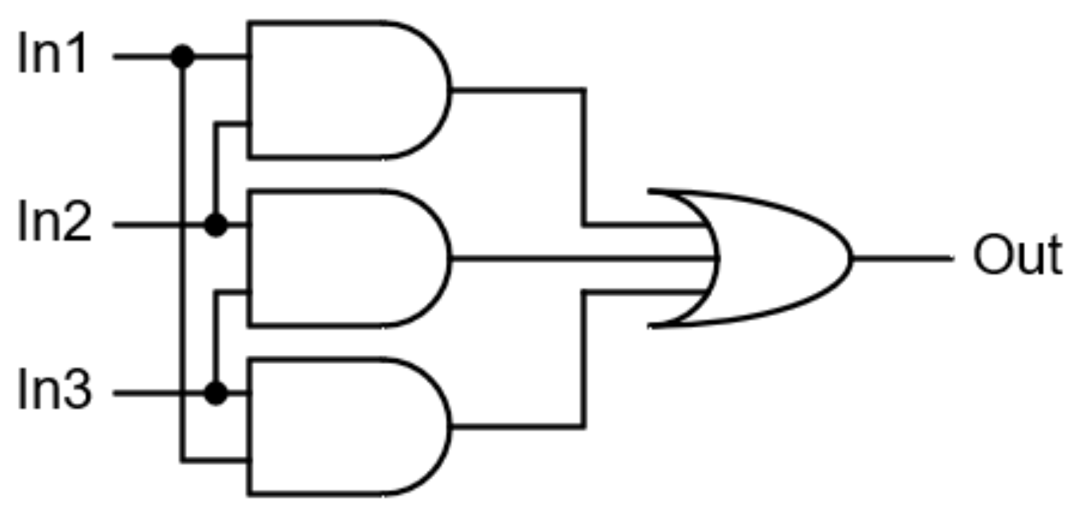
The classical form of the voter is shown in
Figure 3 [
41]. Naturally, the output ‘Out’ has inputs In1, In2 and In3, which is a majority. As can be seen, the classic form of the voter is very simple. This raises the question of its reliability. It seems that the main source of malfunctioning of the voter may be changes to its structure due to errors in the configuration memory of the FPGA chip. This memory is generally protected by a scrubbing mechanism. Theoretically, voter errors are possible, but given the mechanisms for repairing configuration memories, we assume their reliability in the remainder of this paper.
In general, there are many different designs of TMR voters: Kshirsagar voter [
42], the Balasubramanian voter [
43], the Ban and Naviner voter [
44], or the Mux-based voter [
45]. Additionally, in [
46], self-checking voting circuit for increased reliability consensus voting on FPGAs is shown. Other solutions should also be mentioned here, such as FPGA and FPAAs (Field Programmable Analog Array), which means it is a mixed-signal diverse redundancy [
47], scan-chain-based multiple error recovery technique [
48].
The main objective of TMR implementation is the need to introduce fault mitigation in critical circuits. Unfortunately, this approach is subject to some drawbacks. The main disadvantages of this approach are the significant increase in the logical structure obtained and the increased energy consumption. However, there are methods to reduce the increased area [
49,
50]. The results from the paper [
51] show that quadded logic, state machine encoding, and temporal redundancy provides greater reliability and often require more resources than TMR. In opposite, the high-level synthesis approach for scheduling and binding to provide attractive tradeoffs between area, performance, and redundancy presented in [
52] shows resource savings in relation to TMR. It is important to adopt a strategy for the use of TMR in the design [
53].
Approaches to triple modular redundancy, and indeed to the location of the voter, are many [
54,
55].
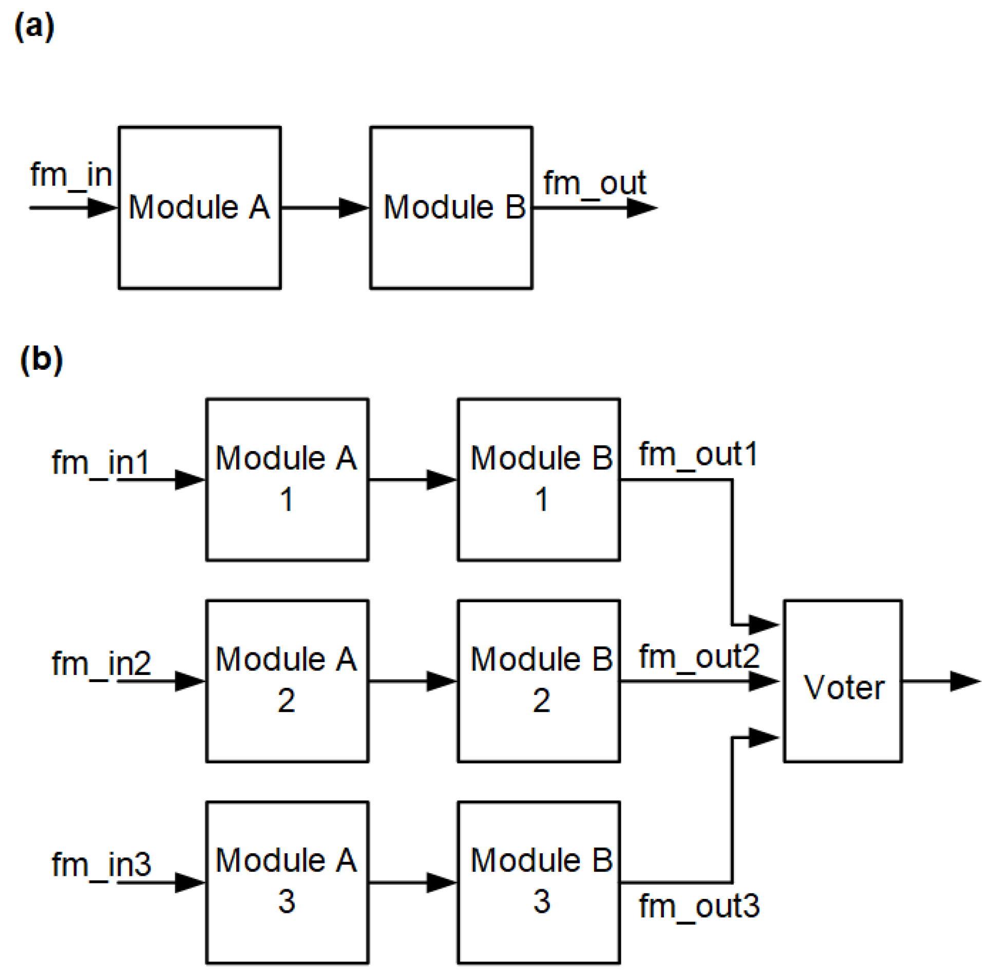
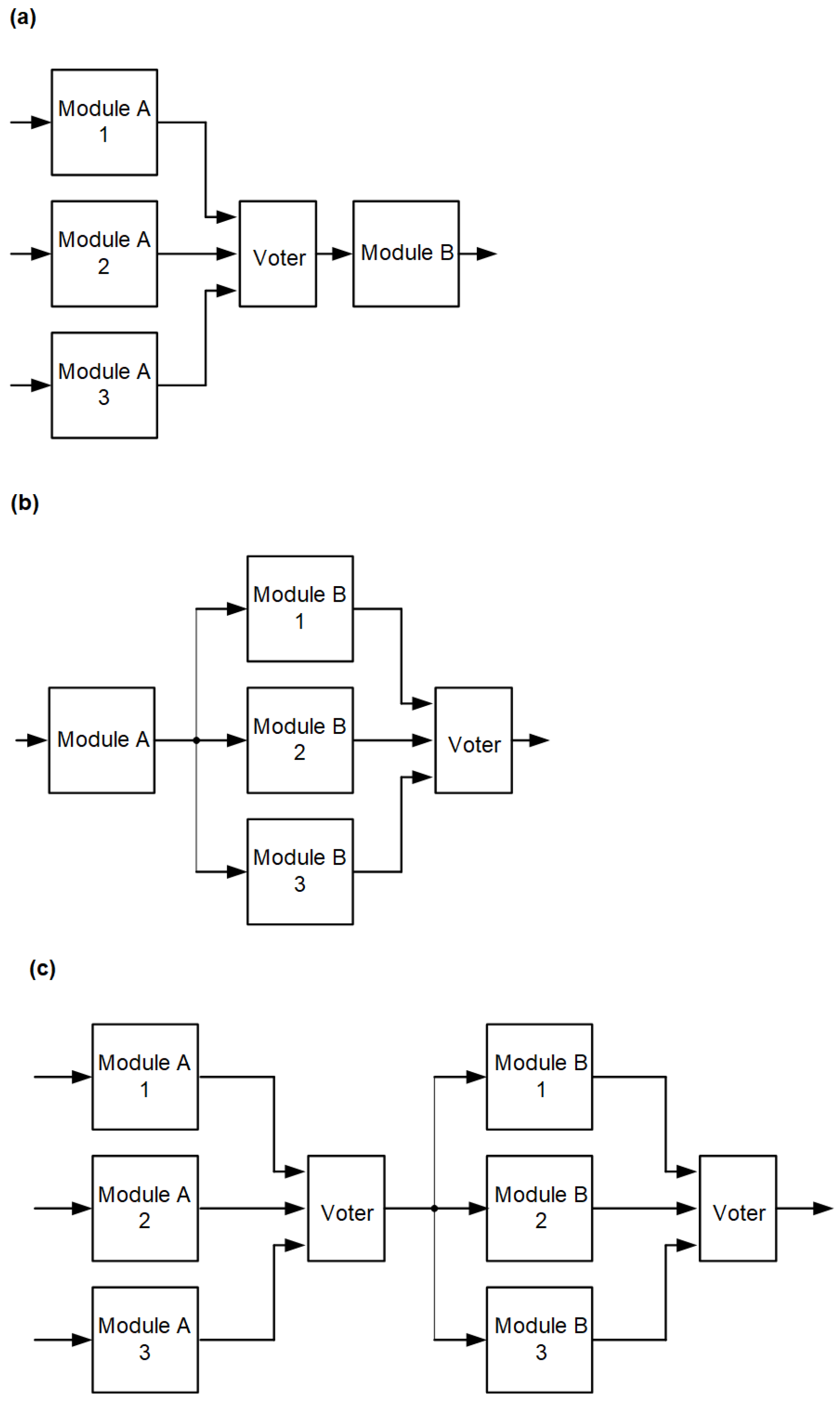
The location of the voter is important for the functionality of the system. In the case of combinatorial or combinatorial systems with register output (no feedback), this is less important, although there are also several possibilities here. Consider the combination of two functional blocks as a fragment of a larger system (
Figure 4a, e.g., instruction decoder and arithmetic-logic unit in microprocessor). Let these functional blocks be combinatorial modules. The most obvious solution is to triplicate the modules understood as an overall/single block and locate the voter at the output—
Figure 4b.
It is easy to imagine a situation in which one of the blocks (or both) is critical to the criticality of the system, or one of the blocks occupies a noticeably larger area of the system and is, therefore, more exposed to radiation effects. In such a situation, redundancy can be applied to either or both modules, as shown in
Figure 5.
The combinatorial circuit in
Figure 5a is mitigating for the circuit associated with module A, the Voter in this circuit realizes the majority selection of signals from individual modules A. Module B is not protected by the corresponding redundancy. In
Figure 5b, the opposite situation occurs, in which module B is redundant and module A is not protected. In the case of
Figure 5c, both modules are redundant.
The situation is more complicated for sequential systems (with feedback). The essence and comparison of triple modular redundancy in FSM will be shown in the next section.
The impact of SET on internal FSM state with voter is presented in
Figure 6. One transition block
outputs with 1001 state instead of 1011, while others outputs with 1011. The majority voting gives 1011, so the correct state is latched in the state register DFF.
3. Triple Modular Redundancy in FSMs
The use of triple redundancy in sequential systems requires deeper analysis. The operation of such systems is determined not only by the input state, but also by the previous state. In view of this, an error in a circuit/module can cause a whole series of incorrect states of such a circuit (
Figure 2). Placing a voter as in
Figure 6 does not solve all of these problems. Consideration needs to be given to what architecture with voter/voters will effectively achieve the objectives.
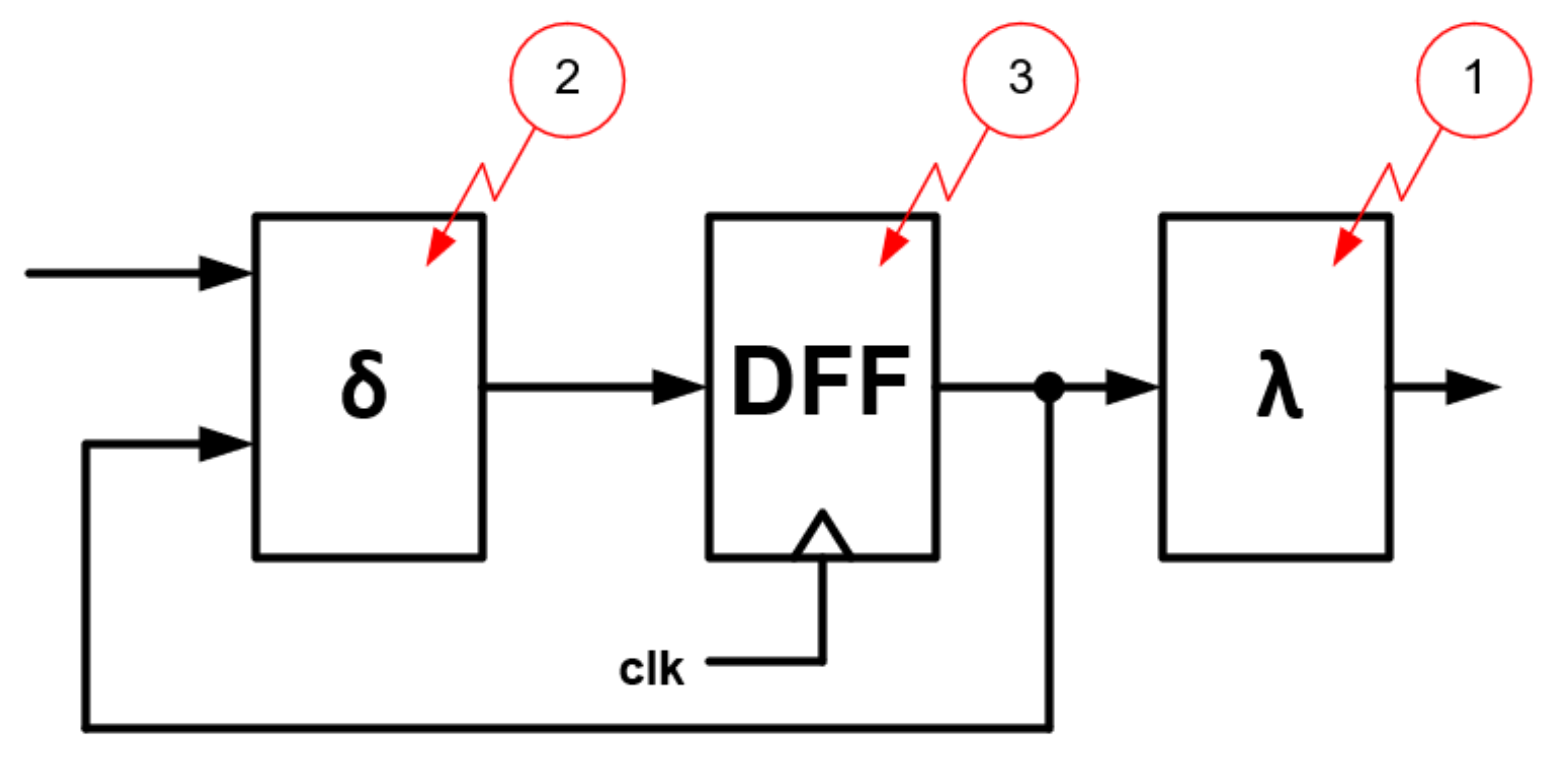
Let us consider an example of the implementation of an FSM according to Moore’s architecture.
Figure 7 also shows the three points at which errors will be injected, assuming they are single errors.
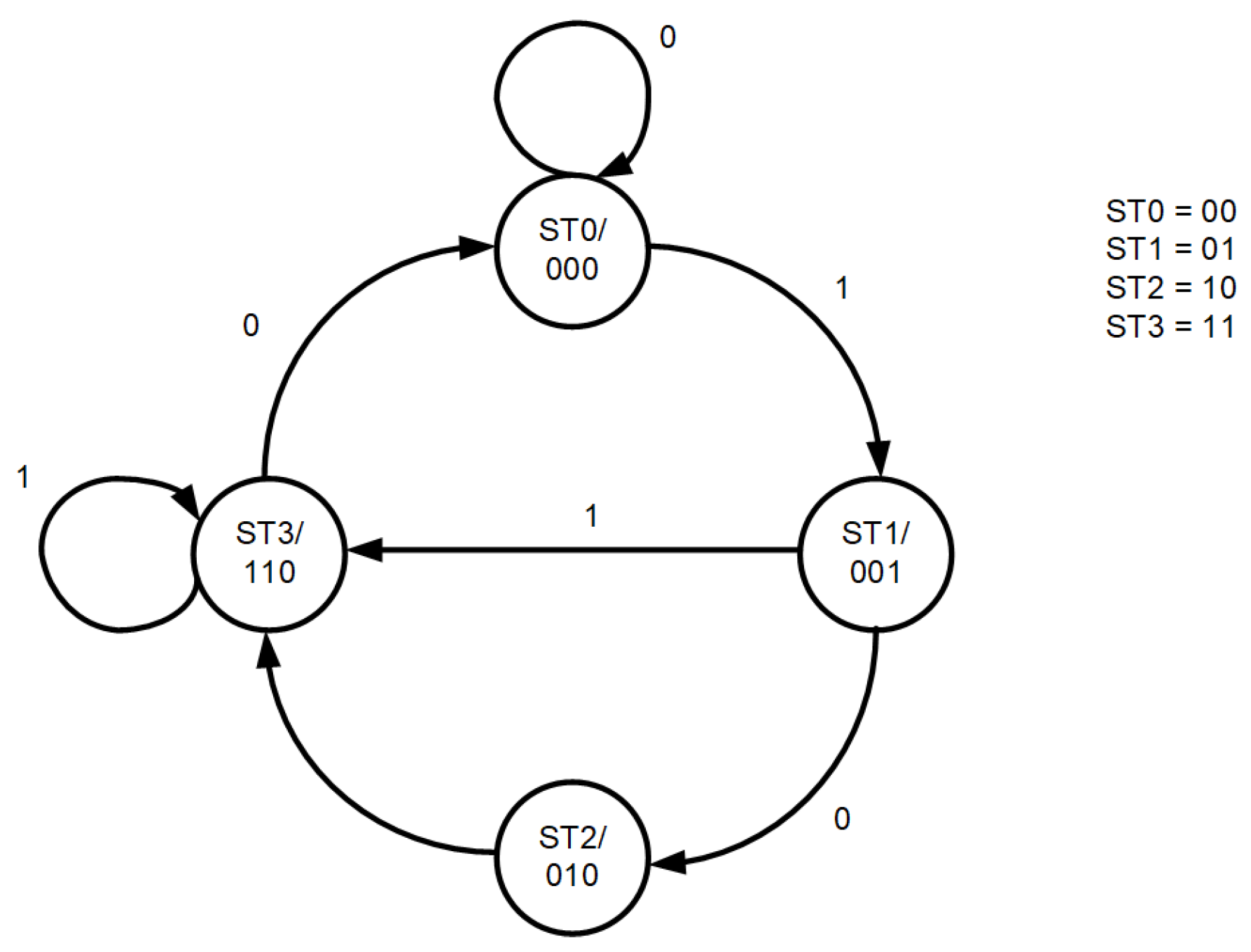
Let the FSM follow the simple graph shown in
Figure 8. Let us consider the behavior of this FSM when an error is injected at three different locations (as in
Figure 7). Let us assume that the FSM is in state
at the beginning each time and the input is state in 1.
Let an error be injected in the output block of the FSM (1) on MSB position. In this situation, an incorrect output is realized—the output state is 101. For the second time, let an error be injected into the transition block (2) on the least significant bit: from 1 to 0. In this situation, the FSM will transition to state instead of transitioning to state. The third time, let an error be injected into the state register DFF (3) on the least significant bit: from 1 to 0. In this situation, the FSM behaves as if it was in the state instead of the state, so the transition to the state will be realized.
Consider these error injection options in FSMs with triple modular redundancy according to different architectures. For simplicity, let us assume that the initial conditions are always the same: the FSM/FSMs is/are in state
and the input is in state 1. Error injector numbers (1)–(3) will be marked as shown in
Figure 7. The considerations presented in the following subsections include assumptions of the occurrence of a single error and do not take into account the situation in which the voter is subject to errors. Depending on the placement of the voter and the choice of FSM blocks subjected to redundancy, several error effects mitigation models can be distinguished.
The models presented in the following sections are shown for Moore’s FSM. Of course, these models are analogous to Mealy’s structure, but drawing an additional connection would obscure the individual figures unnecessarily. However, the experiments presented in
Section 5 include both Moore and Mealy benchmarks.
3.1. Model 1—Triplicated State Register DFF
The first model analyzed represents a situation in which the state register DFF is triplicated. The architecture of the FSM is shown in
Figure 9.
- (1)
Injecting an error at the output block of the FSM will cause the output error.
- (2)
If the error is injected into the transition block , all three registers will latch the incorrect state.
- (3)
If the error is injected into the state register DFF, then voter will operate and the FSM will not only produce the correct output state, but also the next state for all state registers—the ‘broken’ FSM will return to the correct cycle.
TMR can be implemented independently on the output block.
3.2. Model 2—Triplicated Transition Block and State Register DFF
Model 2 corresponds to a situation where TMR is implemented on the transition block
together with state register DFF—
Figure 10.
- (1)
As before, if an error occurs in the output block , the output will be corrupted.
- (2)
If an error is injected into one of the three transition block , the appropriate state register will latch the wrong value and this FSM will be in the wrong state. However, the voter at the output of the state registers will verify this and fix it in the next clock.
- (3)
If the error is in the state register DFF, two of the three transition blocks will still operate correctly, which will cause the third FSM to return to the correct cycle as well.
TMR can be implemented independently on the output block.
3.3. Model 3—Triplicated Transition Block and Independently Registered
In the case of Model 3, the TMR circuit appears primarily on the transition blocks
and each state is latched in a separate state register DFF. The situation is shown in
Figure 11.
- (1)
If the error occurs in the output block , it will be mitigated due to voter on the output.
- (2)
If the error is injected into one of the three transition blocks , the voter at the output of this block will correct the value based on the data from the other two next state logic blocks and each FSM will move to the correct state.
- (3)
Conversely, with an error on the state register DFF, two of the three transition block still operate correctly, which will cause the third FSM to return to the correct cycle as well. The output is subject to voting, so this will also be appropriate.
The output block can, of course, be replaced by a single one—analogous to the voter of the state register DFF in Model 2.
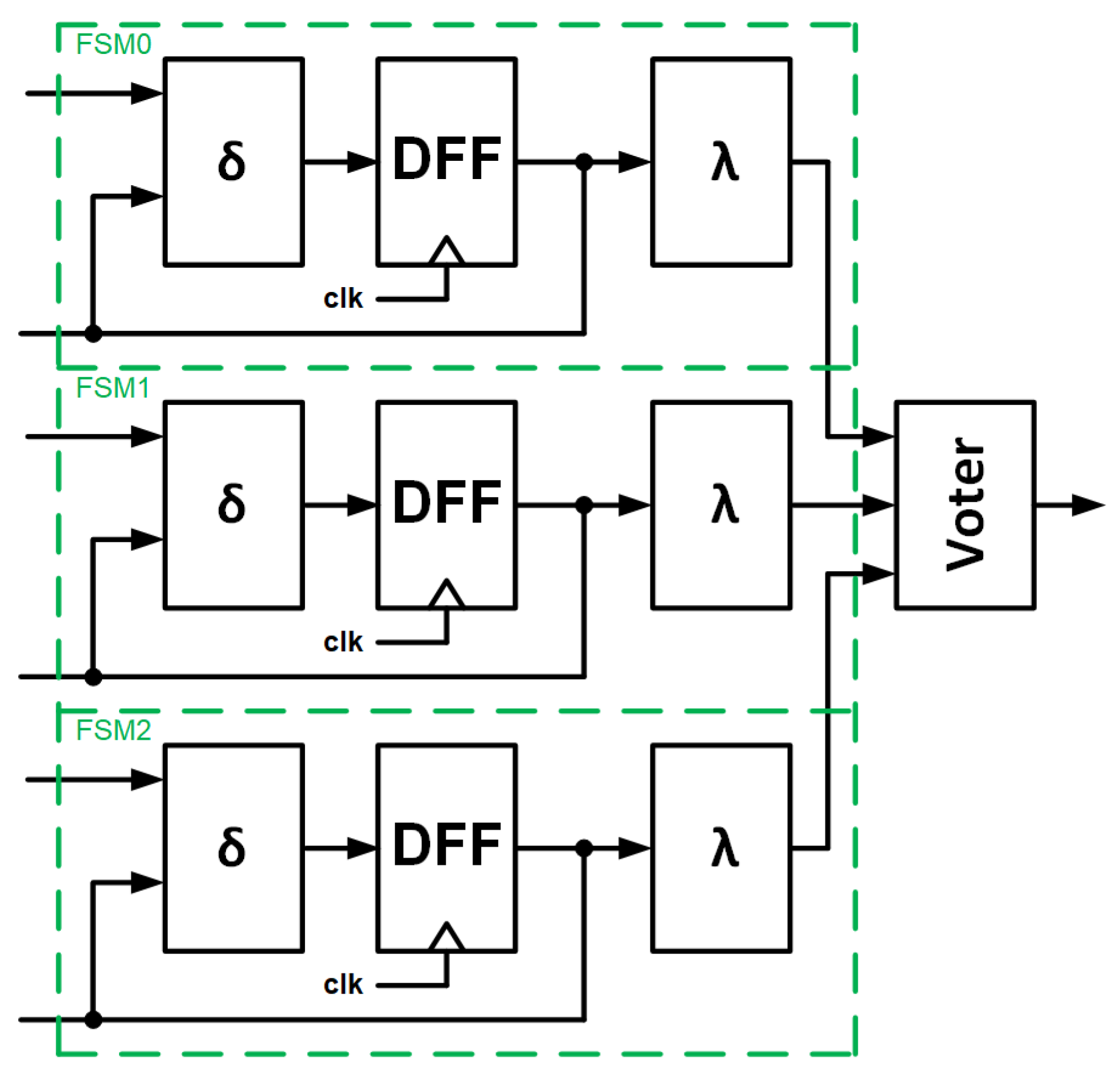
3.4. Model 4—Triplicated the Whole FSM
Model 4 presents a situation in which the entire FSM is triplicated. Here, we are dealing with a situation in which we treat the FSM as a black box. A diagram of the architecture is shown in
Figure 12.
- (1)
If the error occurs in the output block , it will be mitigated due to the voter;
- (2,3)
If the errors cause FSM to go to the wrong state, and hence, have an incorrect cycle, the voter will correct the operation of the entire block and give the correct result.
However, the faulty FSM will not be corrected and will remain in the wrong cycle. If an error is injected into any of the others FSMs, there will potentially be two FSMs operating in the wrong cycle and the results of the entire block will be incorrect.
4. FSM Mitigation Architectures Summary
An analysis of the functionality of the presented models is summarized in
Table 2.
In Model 1, a significant drawback was the inability to correct an error injected into the transition block . It is essential to detect errors and correct the individual FSM or the entire system.
Models 1 and 2 have very similar properties. In both cases, they have the ability to correct errors (2) and (3), and are self-correcting. Due to the architecture, the TMR is also performed on output block in Model 3, so injecting an error into the output block will not affect the output of the whole system.
The design shown in Model 4 is dangerous, because the system has no self-correcting capacity. After an error, the FSM starts to work on a different cycle. In such a situation, in addition to the classic voter, the circuit should be equipped with error detection, which should result in resetting of each FSM (if such a possibility exists) or a more complex system for setting the internal state of a malfunctioning FSM during operation. The FSM outputs are realized by a combinatorial circuit, so the TMR application rules are not critical. Even if the block of outputs is synchronized, the output essentially depends on the state of the FSM and the correcting state is crucial for the whole system.
The use of the method of encoding the internal states of an FSM requires a separate discussion. The way the internal states are encoded has a strong influence on the number of FFs and the number of LUTs (Look-up Tables; most modern FPGAs). Natural binary code or Gray code are characterized by their high compactness in terms of codeword. This leads to a small number of FFs but is paid for by a rather complex transition function, which increases the number of LUTs. A characteristic of Gray code is that the code distance is always equal to 1, which makes it easier to search for potential errors. However, this is only true in cyclic graphs, which are not typical in FSMs. More advanced solutions in terms of reliability would, however, require the introduction of redundant bits (error detection and correction), which would, in turn, lead to an increase in the number of FFs and LUTs. For LUT-type circuits, the most commonly used method of encoding states is one-hot because of the simple decoding and efficient functional decomposition methods. If any bit of the state is changed, the FSM immediately has an invalid internal state (unlike other coding methods, where the state may have the correct bit pattern). On the other hand, a higher number of FFs is required compared to compact coding. It is, therefore, difficult to identify the optimum coding here. Moreover, in this situation, depending on the method of describing the FSM in HDL and the synthesis algorithm used, the FSM will move to the wrong state or correct itself to the initial state. Either way, it will not remain in the correct cycle. One-hot encoding is used for SEU reliability [
56].
A way of automatically embedding TMR into a design is to use tools for automated high-reliability synthesis. Some commercially available tools for FPGAs are AMD/Xilinx XTMR, Synopsys Synplify Premier, and Siemens Precision Hi-Rel.
It must be clearly emphasized that triple modular redundancy is only one element in the mitigation of the effects of radiation. It does not in any way protect the system if an error is injected into the input of the FSM, much less if the error occurs on the clock tree. In the latter case, a circuit based in some way on the SKEW phenomenon and presented in the thesis [
57] or in paper [
58] can be used.
According to the authors, the efficiency of FSM implementations containing TMRs depends on a number of factors, such as power consumption, the number of resources used, and the ability to repair errors. By power, the authors mean dynamic power, which is technology-independent and can be influenced at the implementation stage. The number of resources used in the case of FPGA devices is the number of LUT blocks with which the various functions are implemented. Naturally, the FPGA device also has other logical resources, but the ideas described in the article do not affect them. Error correction capability should be interpreted literally (either the circuit is capable of recovering from faults or it is not, i.e., it does not contain mitigation mechanisms).
5. Experimental Results
A number of experiments have been carried out to compare different methods of mitigating FSMs’ error effects. The aim of this comparison is to determine the best solutions in terms of the number of LUT blocks, the number of logic levels, and, especially importantly, the dynamic power consumed. The most popular set of benchmarks describing FSMs [
59] was used. Based on the benchmarks described in kiss2 format, descriptions of the transition functions and outputs were extracted and converted to Verilog HDL. These HDL descriptions are supplemented by flip-flops. Their number depends on how the internal states are encoded. Since most often the internal states in the kiss2 format are represented in symbolic form, the one-hot coding was adopted as the most universal and most common for FPGAs. In one case (s27), the encoding was already imposed on the kiss2 format. In this situation, the authors decided to leave the original encoding in place. Moreover, the description of each benchmark is supplemented by TMR voters. The way they are included is determined by one of five models, where Model 0 is an FSM completely devoid of TMR voters (
Figure 1) and Models 1–4 are presented in
Section 3.1,
Section 3.2,
Section 3.3 and
Section 3.4, respectively.
The academic synthesis tool ABC [
60] targeting LUT blocks with four inputs (
) was used for the experiments. The benchmark parameters, i.e., the number of inputs, the number of outputs, and the number of internal states of the FSM, are presented in
Table 3. The results obtained are summarized in the form of
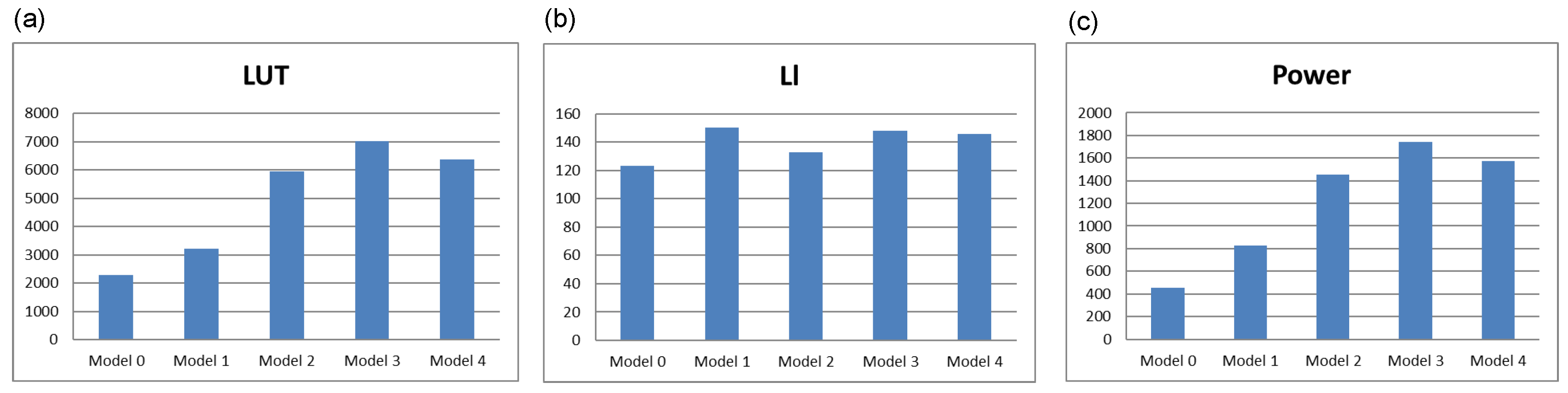
Table 4. The number of flip-flops ‘FF’, the number of LUT blocks ‘LUT’, and the number of logic levels ‘Ll’ were determined. In addition, the value of ‘Power’ obtained from the ABC system, associated with switching activity (dynamic power for constant values of frequency and supply voltage), is shown. The last row contains the values of the sums of the individual quantities summarized in the table. These are shown as graphs in
Figure 13.
Comparing the results obtained, the number of LUT blocks (
Figure 13a) utilized for triplication of combinatorial blocks (Models 2, 3 and 4) shows a significant increase in the use of logic resources, which seems natural. It can also be seen that Model 4 uses lower resources than Model 3. This means that replicating entire FSM is more efficient in terms of the number of LUT blocks than deep interference with the architecture, as in Model 3. Taking the model without redundancy (Model 0) as the reference model, the utilization of logic resources can be determined against this model. Relating this to the number of FFs, it can be seen that in all other models, there is a tripling of the number of FFs. In contrast, the number of LUT blocks is, respectively, 1.41 (Model 1), 2.61 (Model 2), 3.08 (Model 3), and 2.80 (Model 4) relative to Model 0. When comparing the results obtained in terms of the number of logical levels (
Figure 13b), it is difficult to draw clear conclusions. It can be seen that the use of TMR voters increases the number of logical levels, which is in line with expectations. In the case of power (
Figure 13c), it is easy to see the similarity to the graph of
Figure 13a—Model 4 performs better than Model 3.
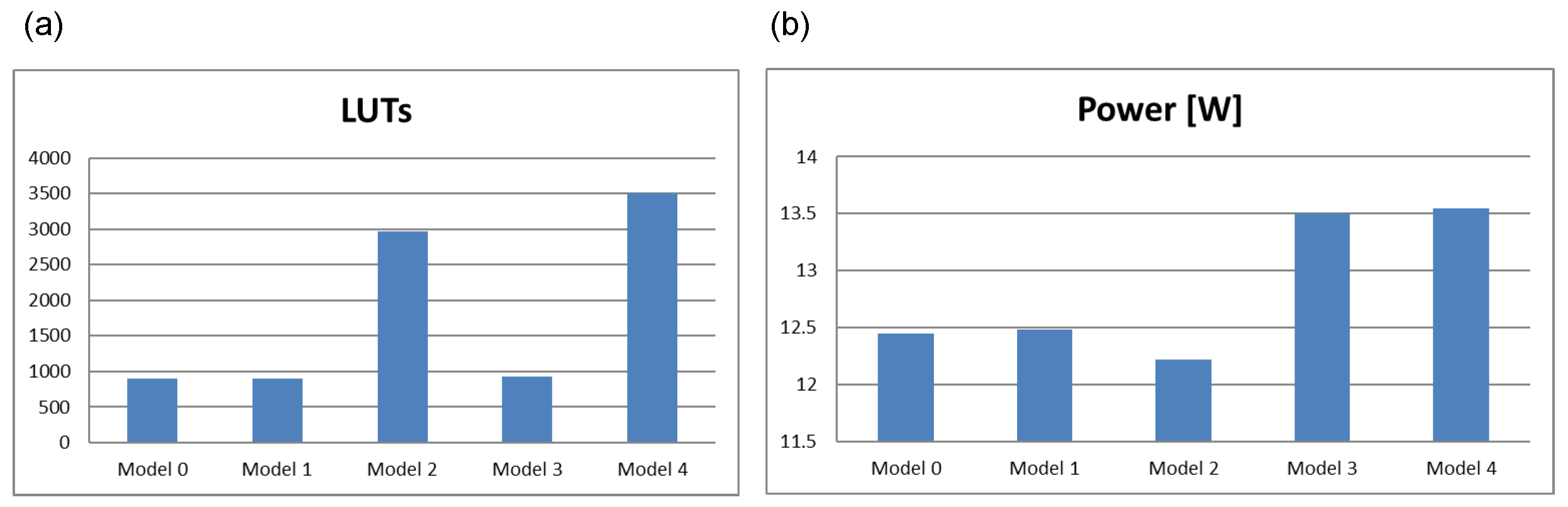
The authors additionally performed experiments in the commercial Vivado system (AMD). The synthesis was targeted at the logic blocks of 7-series FPGAs (Artix-7). The results are summarized in
Table 5.
Table 5 is organized similarly to
Table 4 except that only the number of LUT blocks ‘LUT’ and the dynamic power ‘Power’ expressed in watts are given for each model. These parameters were read from the respective reports after the synthesis and implementation process. The values of the totals are presented as graphs in
Figure 14.
It is difficult to draw clear conclusions from
Figure 14a. It can be seen that the results for Model 3 are somehow distorted (the complex redundancy of model 3 gives virtually the same results as the FSM in its simplest form—Model 0). The reason for this may be the complex logic resource sharing and optimization algorithms. It should be noted that the optimization process is a multi-stage process. It also includes placement and routing. This means that, in many cases, optimization in terms of placement or routing of connections can spoil the results of optimization in terms of the number of LUTs or power. The results for Models 2 and 4 seem reliable, but it is difficult to draw too far-reaching conclusions here. The situation is slightly different for power (
Figure 14b). Here, as expected, the highest power is found for Models 3 and 4. An important conclusion from the analysis of this graph is that a significant expansion of the circuit with redundancy elements does not result in a significant increase in power.
In the authors’ opinion, it is more valuable and reliable to compare the results in the ABC system. The ABC algorithm is publicly available, whereas the Vivado system is a commercial tool and some of its algorithms are implicit. The synthesis in Vivado targets logic blocks with significant flexibility in the number of inputs. In ABC, fixed blocks with are assumed. Taking this into account in the FSM synthesis (ABC), the use of TMR voters for safest architectures (Model 3 or 4) gives the most efficient results for model 4 (full triplication of the FSM).
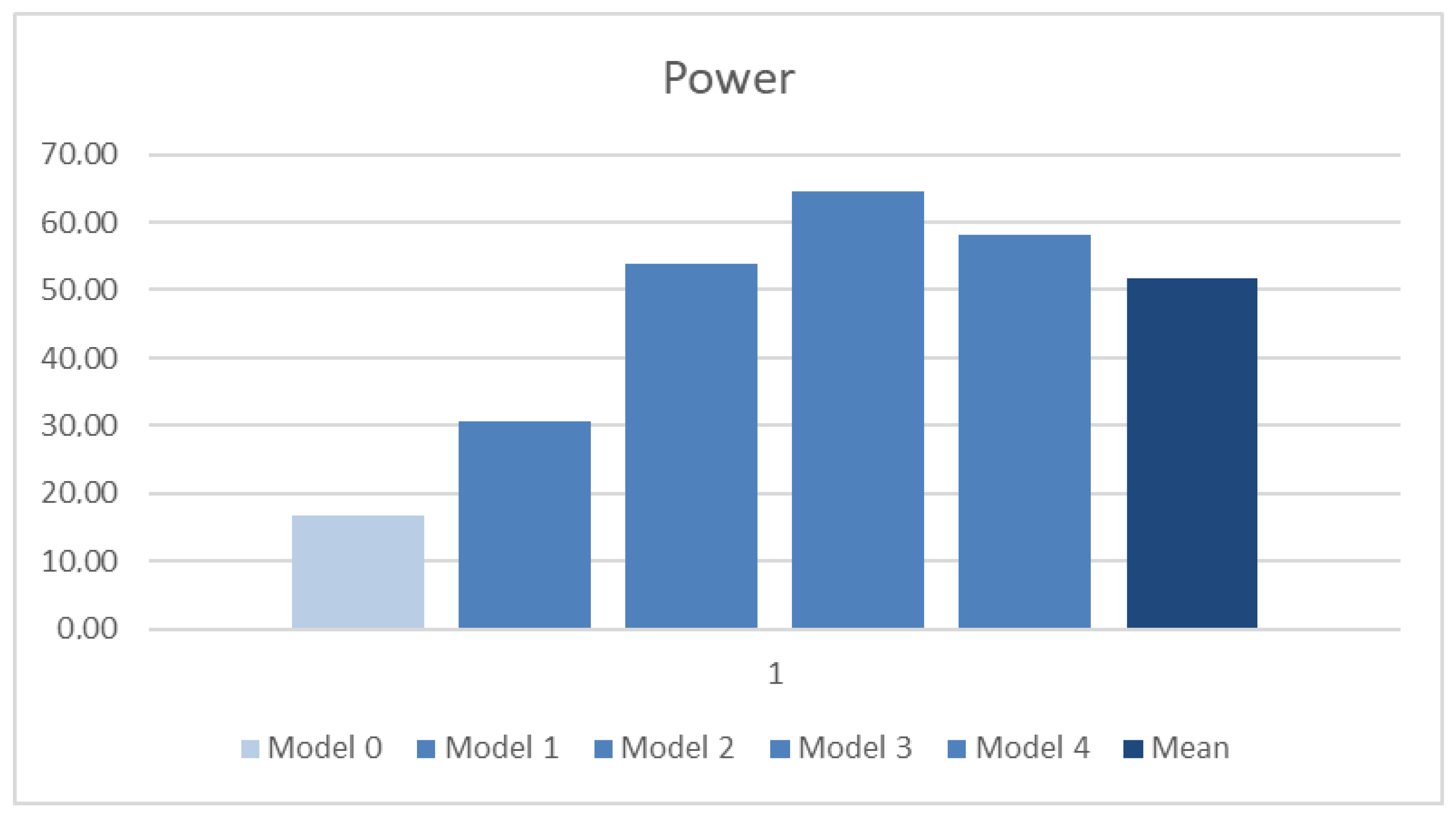
The results obtained for ABC and Vivado power are further presented in
Table 6 and
Table 7, whereby the rightmost column corresponds to the arithmetic mean calculated for the TMR-derived models (Model 1–4).
The results of the average obtained from all benchmarks for each model are presented in the last row of the table and in the bar charts in
Figure 15 and
Figure 16, respectively.
For the ABC system, the trend of individual benchmarks is maintained, with Model 3 having higher values than Model 4 (
Table 6). The results of the average reflect this well—
Figure 15. For the Vivado system, the individual cases (
Table 7) vary quite a bit and do not preserve a common trend. In view of this, the average for Models 3 and 4 is very similar. It should be noted that the mean values for Model 3 and 4 are comparable and clearly worse than the average (
Figure 16).
6. Conclusions
This paper presents a performance comparison of error effects mitigation methods for FSMs using triple modular redundancy, implemented in FPGAs. The methods focus on the ability to recover from SEE effects by introducing system redundancy, with various aspects related to the additional logic part utilization. The paper does not consider the effects of the total dose effect, and omits aspects related to the protection of the voter itself, or the configuration memory of the FPGA chip. The experiments carried out included synthesis in academic and commercial environments.
Considering safety, two models come to the fore: where transition block together with state register DFF is triplicated and transition block is triplicated and independently registered (Model 2 and Model 3, respectively).
Considering the results from the academic ABC system, Model 2 is superior to Model 3 for area utilization (LUT), number of logic levels, and power dissipation. However, it should be noted that in Model 3, there is an embedded TMR for the output block, so these results are expected. In many test cases, differences in logic occupancy or power dissipation are negligible.
The simplest mitigation model (Model 4) is based on triple redundancy of entire FSMs on a black box basis. Clearly, the results in relation to Model 2 and Model 3 are not very different, but it should also be made clear that this model requires resetting the system after an error (or at least setting the correct state in an erroneous FSM). Otherwise, errors can accumulate, as this structure has no auto-correction properties.
Described methods may be taken into account for safety-critical FPGA-based designs.
Author Contributions
Conceptualisation, M.K. and R.C.; methodology, M.K. and R.C.; software, M.K.; formal analysis, M.K. and R.C.; investigation, M.K. and R.C.; resources, M.K. and R.C.; data curation, M.K.; writing—original draft preparation, M.K. and R.C.; writing—review and editing, M.K. and R.C.; visualization, M.K. and R.C.; supervision, M.K.; funding acquisition, M.K. and R.C. All authors have read and agreed to the published version of the manuscript.
Funding
This research was partially supported by European Space Agency (ESA Contract No. 4000132609/20/NL/FE) and by the Polish Ministry of Science and Higher Education funding for statutory activities (BK-250/Rau-12/2025).
Institutional Review Board Statement
Not applicable.
Informed Consent Statement
Not applicable.
Data Availability Statement
The original contributions presented in the study are included in the article; further inquiries can be directed to the corresponding author.
Conflicts of Interest
Authors Marcin Kubica and Robert Czerwinski were employed by the company KP Labs. The remaining authors declare that the research was conducted in the absence of any commercial or financial relationships that could be construed as a potential conflict of interest.
Abbreviations
The following abbreviations are used in this manuscript:
| CE | Clock Enable |
| DFF | D Flip-Flop |
| ECC | Error Checking and Correction |
| ESA | European Space Agency |
| FPGA | Field Programmable Gate Arrays |
| FSM | Finite State Machine |
| HDL | Hardware Description Language |
| LUT | Look-up Table |
| SEB | Single-event burnout |
| SEE | Single-Event Effect |
| SEFI | Single-event function interrupts |
| SEGR | Single-event gate rupture |
| SEL | Single-event latch-up |
| SET | Single-event transient |
| SEU | Single-event upset |
| TMR | Triple modular redundancy |
References
- Galkin, P.; Umiarov, R.; Grigorieva, O.; Ageyev, D. Approaches for Safety-Critical Embedded Systems and Telecommunication Systems Design for Avionics Based on FPGA. In Proceedings of the 2019 IEEE International Scientific-Practical Conference Problems of Infocommunications, Science and Technology (PIC S&T), Kyiv, Ukraine, 8–11 October 2019; pp. 391–396. [Google Scholar] [CrossRef]
- Ball, J.E.; Tang, B. Machine Learning and Embedded Computing in Advanced Driver Assistance Systems (ADAS). Electronics 2019, 8, 748. [Google Scholar] [CrossRef]
- Baumann, R.; Kruckmeyer, K. Radiation Handbook for Electronics; Texas Instruments: Dallas, TX, USA, 2020. [Google Scholar]
- White, D. Considerations Surrounding Single Event Effects in FPGAs, ASICs, and Processors, v1.0.1 ed.; Xilinx Inc.: San Jose, CA, USA, 2012. [Google Scholar]
- Hatefinasab, S.; Rodriguez, N.; García, A.; Castillo, E. Low-Cost Soft Error Robust Hardened D-Latch for CMOS Technology Circuit. Electronics 2021, 10, 1256. [Google Scholar] [CrossRef]
- Actel. Radiation-Tolerant ProASIC3 FPGAs Radiation Effects; Actel: Aliso Viejo, CA, USA, 2010. [Google Scholar]
- Adell, P.; Allen, G. Assessing and Mitigating Radiation Effects in Xilinx FPGAs; Technical Report; Jet Propulsion Laboratory: Pasadena, CA, USA, 2008. [Google Scholar]
- Hall, F. Fault Tolerant Design Implementation on Radiation Hardened by Design SRAM-Based FPGAs. Master’s Thesis, Massachusetts Institute of Technology, Cambridge, MA, USA, 2013. Available online: https://dspace.mit.edu/handle/1721.1/82490 (accessed on 1 June 2025).
- Zheng, S.; You, H.; He, G.; Wang, Q.; Si, T.; Jiang, J.; Jin, J.; Jing, N. A Rapid Scrubbing Technique for SEU Mitigation on SRAM-Based FPGAs. In Proceedings of the IEEE International Symposium on Circuits and Systems (ISCAS), Sapporo, Japan, 26–29 May 2019; pp. 1–5. [Google Scholar] [CrossRef]
- Kumar, M.; Digdarsini, D.; Misra, N.; Ram, T.V.S. SEU mitigation of Rad-Tolerant Xilinx FPGA using external scrubbing for geostationary mission. In Proceedings of the 4th International Conference on Signal Processing and Integrated Networks (SPIN), Noida, India, 2–3 February 2017; pp. 414–418. [Google Scholar] [CrossRef]
- Ruano, Ó.; García-Herrero, F.; Aranda, L.; Sánchez-Macián, A.; Rodriguez, L.; Maestro, J. Fault Injection Emulation for Systems in FPGAs: Tools, Techniques and Methodology, a Tutorial. Sensors 2021, 21, 1392. [Google Scholar] [CrossRef] [PubMed]
- He, W.; Wang, Y.; Xing, K.; Chen, L. SEU readback interval strategy of SRAM-based FPGA for space application. In Proceedings of the IEEE International Conference on Computer Science and Automation Engineering, Shanghai, China, 10–12 June 2011; pp. 238–241. [Google Scholar] [CrossRef]
- Gantel, L.; Berthet, Q.; Amri, E.; Karlov, A.; Upegui, A. Fault-Tolerant FPGA-Based Nanosatellite Balancing High-Performance and Safety for Cryptography Application. Electronics 2021, 10, 2148. [Google Scholar] [CrossRef]
- Alacchi, A.; Giacomin, E.; Temple, S.; Gauchi, R.; Wirthlin, M.; Gaillardon, P. Low Latency SEU Detection in FPGA CRAM with In-Memory ECC Checking. IEEE Trans. Circuits Syst. Regul. Pap. 2023, 70, 2028–2036. [Google Scholar] [CrossRef]
- Hamming, R.W. Error detecting and error correcting codes. Bell Syst. Tech. J. 1950, 29, 147–160. [Google Scholar] [CrossRef]
- Reed, I.S.; Solomon, G. Polynomial Codes over Certain Finite Fields. J. Soc. Ind. Appl. Math. 1960, 8, 300–304. [Google Scholar] [CrossRef]
- Leong, C.; Semião, J.; Santos, M.; Teixeira, I.; Teixeira, J.; Batista, A.; Gonçalves, B.; Marques, J. Fast radiation monitoring in FPGA-based designs. In Proceedings of the 2015 Conference on Design of Circuits and Integrated Systems (DCIS), Estoril, Portugal, 25–27 November 2015; pp. 1–6. [Google Scholar] [CrossRef]
- Mahmoud, D.G.; Alkady, G.I.; Amer, H.H.; Daoud, R.M.; Adly, I.; Essam, Y.; Ismail, H.A.; Sorour, K.N. Fault secure FPGA-based TMR voter. In Proceedings of the 7th Mediterranean Conference on Embedded Computing (MECO), Budva, Montenegro, 10–14 June 2018; pp. 1–4. [Google Scholar] [CrossRef]
- Benites, L.A.C.; Kastensmidt, F.L. Automated design flow for applying Triple Modular Redundancy (TMR) in complex digital circuits. In Proceedings of the IEEE 19th Latin-American Test Symposium (LATS), Sao Paulo, Brazil, 12–14 March 2018; pp. 1–4. [Google Scholar] [CrossRef]
- Tan, C.; Li, Y.; Cheng, X.; Han, J.; Zeng, X. General Efficient TMR for Combinational Circuit Hardening Against Soft Errors and Improved Multi-Objective Optimization Framework. IEEE Trans. Circuits Syst. Regul. Pap. 2021, 68, 3044–3057. [Google Scholar] [CrossRef]
- Ruano, Ó.; Maestro, J.A.; Reviriego, P. Validation and optimization of TMR protections for circuits in radiation environments. In Proceedings of the 14th IEEE International Symposium on Design and Diagnostics of Electronic Circuits and Systems, Cottbus, Germany, 13–15 April 2011; pp. 399–400. [Google Scholar] [CrossRef]
- Wilson, A.E.; Wirthlin, M.; Baker, N.G. Neutron Radiation Testing of RISC-V TMR Soft Processors on SRAM-Based FPGAs. IEEE Trans. Nucl. Sci. 2021, 70, 603–610. [Google Scholar] [CrossRef]
- Shahbazi, M.; Poure, P.; Saadate, S.; Zolghadri, M.R. FPGA-Based Reconfigurable Control for Fault-Tolerant Back-to-Back Converter Without Redundancy. IEEE Trans. Ind. Electron. 2013, 60, 3360–3371. [Google Scholar] [CrossRef]
- Barkalov, A.; Titarenko, L.; Chmielewski, S. Improving characteristics of LUT-based Moore FSMs. IEEE Access 2020, 8, 155306–155318. [Google Scholar] [CrossRef]
- Barkalov, A.; Titarenko, L.; Mielcarek, K. Improving characteristic of LUT-based Mealy FSMs. Int. J. Appl. Math. Comput. Sci. 2020, 30, 745–759. [Google Scholar] [CrossRef]
- Kubica, M.; Opara, A.; Kania, D. Technology Mapping for LUT-Based FPGA; Springer: Berlin/Heidelberg, Germany, 2021. [Google Scholar]
- Salauyou, V. Area and Performance Estimates of Finite State Machines in Reconfigurable Systems. Appl. Sci. 2024, 14, 1833. [Google Scholar] [CrossRef]
- Cheng, L.; Chen, D.; Wong, M.D.F. DDBDD: Delay-Driven BDD Synthesis for FPGAs. In Proceedings of the 44th ACM/IEEE Design Automation Conference, San Diego, CA, USA, 4–8 June 2007; pp. 910–915. [Google Scholar]
- Kubica, M.; Opara, A.; Kania, D. Logic Synthesis Strategy Oriented to Low Power Optimization. Appl. Sci. 2021, 11, 8797. [Google Scholar] [CrossRef]
- Opara, A.; Kubica, M.; Kania, D. Decomposition Approaches for Power Reduction. IEEE Access 2023, 11, 29417–29429. [Google Scholar] [CrossRef]
- Opara, A.; Kubica, M. Technology mapping of multi–output functions leading to the reduction of dynamic power consumption in FPGAs. Int. J. Appl. Math. Comput. Sci. 2023, 33, 267–284. [Google Scholar] [CrossRef]
- Chattopadhyay, S.; Yadav, P.; Singh, R. Multiplexer Targeted Finite State Machine Encoding for Area and Power Minimization. In Proceedings of the IEEE INDICON, India Annual Conference, Kharagpur, India, 20–22 December 2004. [Google Scholar]
- Kajstura, K.; Kania, D. Binary Tree-based Low Power State Assignment Algorithm. In Proceedings of the 12-th International Conference of Computational Methods in Science and Engineering, ICCMSE 2016, Athens, Greece, 17–20 March 2016. [Google Scholar]
- Amin, R.A.; Amran Hossain, M.S.; Schmid, L.T.; Wiese, V.; Obermaisser, R. Power Efficient Real-Time Traffic Signal Classification for Autonomous Driving Using FPGAs. In Proceedings of the 2024 6th International Conference on Communications, Signal Processing, and Their Applications (ICCSPA), Istanbul, Turkiye, 8–11 July 2024; pp. 1–5. [Google Scholar] [CrossRef]
- Khan, M.I.; da Silva, B. Harnessing FPGA Technology for Energy-Efficient Wearable Medical Devices. Electronics 2024, 13, 4094. [Google Scholar] [CrossRef]
- Verma, G.; Kumar, M.; Khare, V. Low Power Synthesis and Validation of an Embedded Multiplier for FPGA Based Wireless Communication Systems. Wirel. Pers. Commun. 2017, 95, 365–373. [Google Scholar] [CrossRef]
- Kim, Y.; Kim, H.; Yadav, N.; Li, S.; Choi, K.K. Low-Power RTL Code Generation for Advanced CNN Algorithms toward Object Detection in Autonomous Vehicles. Electronics 2020, 9, 478. [Google Scholar] [CrossRef]
- Kubica, M.; Czerwinski, R. Performance Testing of the Triple Modular Redundancy Mitigation Circuit Test Environment Implementation in Field Programmable Gate Array Structures. Appl. Sci. 2024, 14, 8604. [Google Scholar] [CrossRef]
- Aguiar, Y.Q.d.; Wrobel, F.; Autran, J.L.; García Alía, R. Introduction to Single-Event Effects. In Single-Event Effects, from Space to Accelerator Environments:Analysis, Prediction and Hardening by Design; Springer International Publishing: Cham, Switzerland, 2025. [Google Scholar] [CrossRef]
- Kessler, H.; Ferraz, B.; da Rosa, L., Jr.; Aguiar, Y.; Camargo, V. Single Event Transient on Combinational Logic: An Introduction and their Mitigation. J. Integr. Circuits Syst. 2023, 17, 1–9. [Google Scholar] [CrossRef]
- Wang, J. Radiation effects in FPGAs. In Proceedings of the 9th Workshop on Electronics for LHC Experiments, Amsterdam, The Netherlands, 29 September–3 October 2003; pp. 34–43. [Google Scholar] [CrossRef]
- Kshirsagar, R.; Patrikar, R. Design of a novel fault-tolerant voter circuit for TMR implementation to improve reliability in digital circuits. Microelectron. Reliab. 2009, 49, 1573–1577. [Google Scholar] [CrossRef]
- Balasubramanian, P.; Prasad, K. A Fault Tolerance Improved Majority Voter for TMR System Architectures. arXiv 2017, arXiv:1605.03771. [Google Scholar]
- Ban, T.; de Barros Naviner, L.A. A simple fault-tolerant digital voter circuit in TMR nanoarchitectures. In Proceedings of the Proceedings of the 8th IEEE International NEWCAS Conference 2010, Montreal, QC, Canada, 20–23 June 2010; pp. 269–272. [Google Scholar] [CrossRef]
- Deepa, M.; Beulet, P.A.S. An Improvised Voter Architecture for TMR with Reduced Area Overhead. In Proceedings of the 2022 Third International Conference on Intelligent Computing Instrumentation and Control Technologies (ICICICT), Kannur, India, 11–12 August 2022; pp. 1001–1007. [Google Scholar] [CrossRef]
- Afzaal, U.; Lee, J.A. A Self-Checking TMR Voter for Increased Reliability Consensus Voting in FPGAs. IEEE Trans. Nucl. Sci. 2018, 65, 1133–1139. [Google Scholar] [CrossRef]
- Girardey, R.; Hübner, M.; Becker, J. Mixed-Signal Diverse Redundant System for Safety Critical Applications in FPGA. In Proceedings of the 2010 IEEE Computer Society Annual Symposium on VLSI, Lixouri, Greece, 5–7 July 2010; pp. 469–470. [Google Scholar] [CrossRef]
- Ebrahimi, M.; Miremadi, S.G.; Asadi, H.; Fazeli, M. Low-Cost Scan-Chain-Based Technique to Recover Multiple Errors in TMR Systems. IEEE Trans. Very Large Scale Integr. (VLSI) Syst. 2013, 21, 1454–1468. [Google Scholar] [CrossRef]
- Liu, J.; Li, X.; Zhang, J.; Li, J. An Area-Efficient Design of Enhanced Space-Time Redundant DFF (IEST_TMR DFF). In Proceedings of the 7th International Conference on Computer and Communication Systems (ICCCS), Wuhan, China, 22–25 April 2022; pp. 721–726. [Google Scholar] [CrossRef]
- Gomes, I.A.C.; Martins, M.; Reis, A.; Kastensmidt, F.L. Using only redundant modules with approximate logic to reduce drastically area overhead in TMR. In Proceedings of the 16th Latin-American Test Symposium (LATS), Puerto Vallarta, Mexico, 25–27 March 2015; pp. 1–6. [Google Scholar] [CrossRef]
- Morgan, K.S.; McMurtrey, D.L.; Pratt, B.H.; Wirthlin, M.J. A Comparison of TMR with Alternative Fault-Tolerant Design Techniques for FPGAs. IEEE Trans. Nucl. Sci. 2007, 54, 2065–2072. [Google Scholar] [CrossRef]
- Wilson, D.; Shastri, A.; Stitt, G. A High-Level Synthesis Scheduling and Binding Heuristic for FPGA Fault Tolerance. Int. J. Reconfigurable Comput. 2017, 2017, 5419767. [Google Scholar] [CrossRef]
- Hamamatsu, M.; Tsuchiya, T.; Kikuno, T. Finding the Optimal Configuration of a Cascading TMR System. In Proceedings of the 2008 14th IEEE Pacific Rim International Symposium on Dependable Computing, Taipei, Taiwan, 15–17 December 2008; pp. 349–350. [Google Scholar] [CrossRef]
- Khan, K.; Zuiss, B. Verifying Safety-Critical FPGA Designs with Fault Simulation and Injection; White Paper; Synopsys: Sunnyvale, CA, USA, 2023. [Google Scholar]
- Khan, K.; Hoskins, D. Functional Safety for FPGA-Based Hardware Designs; White Paper; Synopsys: Sunnyvale, CA, USA, 2023. [Google Scholar]
- Cassel, M.; Lima, F. Evaluating one-hot encoding finite state machines for SEU reliability in SRAM-based FPGAs. In Proceedings of the 12th IEEE International On-Line Testing Symposium (IOLTS’06), Lake Como, Italy, 10–12 July 2006; p. 6. [Google Scholar] [CrossRef]
- te Slaa, P.S. Fault Tolerant Techniques for Finite State Machines in Hardware Designs. Master’s Thesis, Eindhoven University of Technology, Eindhoven, The Netherlands, 2020. [Google Scholar]
- Petrovic, V.; Krstic, M. Design Flow for Radhard TMR Flip-Flops. In Proceedings of the 2015 IEEE 18th International Symposium on Design and Diagnostics of Electronic Circuits & Systems, Belgrade, Serbia, 22–24 April 2015. [Google Scholar] [CrossRef]
- Collaborative Benchmarking and Experimental Algorythmics Laboratory. LGSynth93 Benchmarks; Collaborative Benchmarking and Experimental Algorythmics Laboratory: Raleigh, NC, USA, 2008. [Google Scholar]
- Berkeley Logic Synthesis Group. ABC: A System for Sequential Synthesis and Verification; Berkeley Logic Synthesis Group: Berkeley, CA, USA, 2005. [Google Scholar]
Figure 1.
The block scheme of FSM.
Figure 1.
The block scheme of FSM.
Figure 2.
Impact of SET on internal FSM state.
Figure 2.
Impact of SET on internal FSM state.
Figure 3.
The classic TMR voter structure.
Figure 3.
The classic TMR voter structure.
Figure 4.
Combinational block consisting of two modules: without TMR (a) and with TMR (b).
Figure 4.
Combinational block consisting of two modules: without TMR (a) and with TMR (b).
Figure 5.
Triple modular redundancy of individual modules in the block: with redundant A module (a), with redundant B module (b), and with A and B redundancy (c).
Figure 5.
Triple modular redundancy of individual modules in the block: with redundant A module (a), with redundant B module (b), and with A and B redundancy (c).
Figure 6.
Impact of SET on internal FSM state (with TMR).
Figure 6.
Impact of SET on internal FSM state (with TMR).
Figure 7.
Moore FSM with error injection points.
Figure 7.
Moore FSM with error injection points.
Figure 8.
State transition graph and state assignment for example FSM.
Figure 8.
State transition graph and state assignment for example FSM.
Figure 9.
Model 1—state register is triplicated.
Figure 9.
Model 1—state register is triplicated.
Figure 10.
Model 2—transition block and state register DFF is triplicated.
Figure 10.
Model 2—transition block and state register DFF is triplicated.
Figure 11.
Model 3—transition block is triplicated and independently registered.
Figure 11.
Model 3—transition block is triplicated and independently registered.
Figure 12.
Model 4—the whole FSM is triplicated.
Figure 12.
Model 4—the whole FSM is triplicated.
Figure 13.
Comparison of synthesis results in the ABC system in terms of the number of LUT blocks (a), number of logic levels (b), and power (c).
Figure 13.
Comparison of synthesis results in the ABC system in terms of the number of LUT blocks (a), number of logic levels (b), and power (c).
Figure 14.
Comparison of synthesis results in the Vivado system in terms of the number of LUT blocks (a) and power (b).
Figure 14.
Comparison of synthesis results in the Vivado system in terms of the number of LUT blocks (a) and power (b).
Figure 15.
Comparison of power results (mean values) in the ABC system.
Figure 15.
Comparison of power results (mean values) in the ABC system.
Figure 16.
Comparison of power results (mean values) in the Vivado system.
Figure 16.
Comparison of power results (mean values) in the Vivado system.
Table 1.
Radiation effects in electronics.
Table 1.
Radiation effects in electronics.
| Type | Cause | Effect |
|---|
| Doste effect | Long-term exposure
to ionising radiation | - Degradation of the crystal structure,
- changes in threshold voltages
- increase in leakage currents
|
| Single Event Effects | High-energy
particle impact | - Single Event Upset (SEU):
change of logical state of a register
- Single Event Transient (SET):
brief electrical pulse
- Single Event Latchup (SEL):
power supply short circuit |
Table 2.
Functionality analysis of each model.
Table 2.
Functionality analysis of each model.
| | Model 1 | Model 2 | Model 3 | Model 4 |
|---|
| Correction capacity (1) | − | − | + | + |
| Correction capacity (2) | − | + | + | + |
| Correction capacity (3) | + | + | + | + |
| Whole-system self-correction | + | + | + | − |
| Necessary to force a reset * | + ** | − | − | + ** |
| Necessary to enforce the correct state by FF SET * | + ** | − | − | + *** |
| Correct output in each internal state | − | + | + | + |
Table 3.
Set of benchmarks.
Table 3.
Set of benchmarks.
| Name | In | Out | State |
|---|
| dk15 | 2 | 5 | 4 |
| lion | 2 | 1 | 4 |
| mc | 3 | 5 | 4 |
| s8 | 4 | 1 | 5 |
| tav | 4 | 4 | 4 |
| train4 | 2 | 1 | 4 |
| bbara | 4 | 2 | 10 |
| bbtas | 2 | 2 | 6 |
| beecount | 3 | 4 | 7 |
| dk14 | 3 | 5 | 7 |
| dk17 | 2 | 3 | 8 |
| dk27 | 1 | 2 | 7 |
| ex5 | 2 | 2 | 9 |
| ex6 | 5 | 8 | 8 |
| ex7 | 2 | 2 | 10 |
| lion9 | 2 | 1 | 9 |
| s27 | 4 | 1 | 3 (6) |
| shiftreg | 1 | 1 | 8 |
| dk512 | 1 | 3 | 15 |
| train11 | 2 | 1 | 11 |
| bbsse | 7 | 7 | 16 |
| cse | 7 | 7 | 16 |
| sse | 7 | 7 | 16 |
| ex2 | 2 | 2 | 19 |
| keyb | 7 | 2 | 19 |
| tma | 7 | 6 | 20 |
| s1 | 8 | 6 | 20 |
Table 4.
Comparison of synthesis results in the ABC system.
Table 4.
Comparison of synthesis results in the ABC system.
| | Model 0 | Model 1 | Model 2 | Model 3 | Model 4 |
|---|
|
Name
|
FF
|
LUT
|
Ll
|
Power
|
FF
|
LUT
|
Ll
|
Power
|
FF
|
LUT
|
Ll
|
Power
|
FF
|
LUT
|
Ll
|
Power
|
FF
|
LUT
|
Ll
|
Power
|
|---|
| dk15 | 4 | 56 | 4 | 30.07 | 12 | 70 | 5 | 35.51 | 12 | 106 | 5 | 61.82 | 12 | 142 | 5 | 82.94 | 12 | 136 | 5 | 75.48 |
| lion | 4 | 19 | 3 | 3.11 | 12 | 30 | 4 | 5.13 | 12 | 53 | 3 | 8.82 | 12 | 56 | 4 | 8.63 | 12 | 50 | 4 | 7.96 |
| mc | 4 | 19 | 3 | 7.46 | 12 | 31 | 4 | 14.74 | 12 | 48 | 4 | 21.24 | 12 | 72 | 4 | 29.62 | 12 | 57 | 4 | 23.83 |
| s8 | 5 | 37 | 5 | 3.56 | 15 | 54 | 5 | 4.72 | 15 | 82 | 4 | 8.68 | 15 | 113 | 6 | 6.8 | 15 | 101 | 6 | 7.12 |
| tav | 4 | 33 | 4 | 30.75 | 12 | 54 | 5 | 63.76 | 12 | 42 | 4 | 52.71 | 12 | 85 | 4 | 94.8 | 12 | 77 | 4 | 81.6 |
| train4 | 4 | 10 | 2 | 1.98 | 12 | 25 | 3 | 4.81 | 12 | 32 | 3 | 5.06 | 12 | 42 | 4 | 6.71 | 12 | 32 | 4 | 5.69 |
| bbara | 10 | 62 | 4 | 10.6 | 30 | 92 | 5 | 14.84 | 30 | 138 | 5 | 22.54 | 30 | 212 | 5 | 33.52 | 30 | 176 | 5 | 27.73 |
| bbtas | 6 | 20 | 3 | 5.74 | 18 | 37 | 4 | 10.78 | 18 | 58 | 3 | 16.75 | 18 | 71 | 4 | 20.15 | 18 | 57 | 3 | 16.26 |
| beecount | 7 | 50 | 5 | 8.47 | 21 | 84 | 6 | 12.59 | 21 | 124 | 5 | 20.29 | 21 | 160 | 5 | 22.78 | 21 | 133 | 5 | 21.07 |
| dk14 | 7 | 100 | 5 | 48.35 | 21 | 147 | 6 | 64.76 | 21 | 228 | 6 | 130.51 | 21 | 319 | 6 | 154.42 | 21 | 302 | 6 | 142.01 |
| dk17 | 8 | 65 | 4 | 45.75 | 24 | 96 | 5 | 64.63 | 24 | 176 | 5 | 112.21 | 24 | 208 | 5 | 148.24 | 24 | 191 | 5 | 131.52 |
| dk27 | 7 | 26 | 3 | 27.5 | 21 | 44 | 4 | 52.45 | 21 | 72 | 3 | 80.48 | 21 | 99 | 4 | 109.81 | 21 | 70 | 4 | 67.84 |
| ex5 | 9 | 58 | 4 | 5.58 | 27 | 83 | 5 | 6.1 | 27 | 162 | 5 | 14.46 | 27 | 188 | 5 | 16.52 | 27 | 169 | 5 | 15.96 |
| ex6 | 8 | 92 | 5 | 61.72 | 24 | 114 | 6 | 71 | 24 | 190 | 6 | 128.92 | 24 | 251 | 6 | 150.85 | 24 | 260 | 6 | 156.51 |
| ex7 | 10 | 60 | 5 | 4.86 | 30 | 93 | 6 | 6.69 | 30 | 179 | 5 | 13.79 | 30 | 207 | 5 | 14.38 | 30 | 179 | 5 | 13.38 |
| lion9 | 9 | 52 | 5 | 4.81 | 27 | 74 | 6 | 6.49 | 27 | 119 | 5 | 9.37 | 27 | 168 | 6 | 12.81 | 27 | 145 | 6 | 12.9 |
| s27 | 3 | 46 | 4 | 14.07 | 9 | 51 | 5 | 15.57 | 9 | 32 | 3 | 10.92 | 9 | 130 | 5 | 36.7 | 9 | 127 | 5 | 35.68 |
| shiftreg | 8 | 29 | 4 | 10.04 | 24 | 55 | 5 | 17.46 | 24 | 62 | 4 | 19.64 | 24 | 109 | 5 | 34.8 | 24 | 86 | 5 | 28.36 |
| dk512 | 15 | 79 | 4 | 4.56 | 45 | 128 | 5 | 91.96 | 45 | 241 | 5 | 164.73 | 45 | 279 | 5 | 196.72 | 45 | 242 | 5 | 167.31 |
| train11 | 11 | 59 | 5 | 5.23 | 33 | 85 | 6 | 6.83 | 33 | 127 | 5 | 7.48 | 33 | 178 | 6 | 12.22 | 33 | 164 | 6 | 12.54 |
| bbsse | 16 | 108 | 5 | 9.89 | 48 | 169 | 6 | 26.14 | 48 | 377 | 6 | 54.74 | 48 | 379 | 6 | 56.48 | 48 | 339 | 7 | 53.54 |
| cse | 16 | 163 | 6 | 15.35 | 48 | 238 | 7 | 30.29 | 48 | 503 | 6 | 59.85 | 48 | 538 | 7 | 62.32 | 48 | 505 | 6 | 59.87 |
| sse | 16 | 121 | 5 | 11.08 | 48 | 189 | 6 | 29.35 | 48 | 374 | 6 | 59.5 | 48 | 397 | 7 | 59.2 | 48 | 361 | 6 | 54.98 |
| ex2 | 19 | 154 | 6 | 11.05 | 57 | 214 | 7 | 13.89 | 57 | 459 | 6 | 30.06 | 57 | 507 | 7 | 31.65 | 57 | 461 | 6 | 30.91 |
| keyb | 19 | 267 | 7 | 37.46 | 57 | 331 | 9 | 73.08 | 57 | 768 | 7 | 159.53 | 57 | 810 | 8 | 167.43 | 57 | 746 | 8 | 157.8 |
| tma | 20 | 158 | 6 | 9.21 | 60 | 230 | 7 | 11.04 | 60 | 392 | 7 | 19.93 | 60 | 504 | 7 | 18.4 | 60 | 458 | 7 | 18.54 |
| s1 | 20 | 334 | 7 | 26.25 | 60 | 399 | 8 | 72.68 | 60 | 800 | 7 | 157.82 | 60 | 799 | 7 | 155.57 | 60 | 757 | 8 | 145.14 |
| Sum | 269 | 2277 | 123 | 454.5 | 807 | 3217 | 150 | 827.29 | 807 | 5944 | 133 | 1451.85 | 807 | 7023 | 148 | 1744.47 | 807 | 6381 | 146 | 1571.53 |
Table 5.
Synthesis results for the Vivado system.
Table 5.
Synthesis results for the Vivado system.
| | Model 0 | Model 1 | Model 2 | Model 3 | Model 4 |
|---|
|
Name
|
LUTs
|
Power [W]
|
LUTs
|
Power [W]
|
LUTs
|
Power [W]
|
LUTs
|
Power [W]
|
LUTs
|
Power [W]
|
|---|
| dk15 | 17 | 1.424 | 17 | 1.424 | 52 | 0.221 | 17 | 1.424 | 59 | 0.347 |
| lion | 5 | 0.092 | 5 | 0.092 | 17 | 0.062 | 5 | 0.092 | 16 | 0.073 |
| mc | 10 | 0.219 | 10 | 0.219 | 25 | 0.347 | 10 | 0.219 | 30 | 0.135 |
| s8 | 18 | 0.101 | 18 | 0.097 | 45 | 0.151 | 18 | 0.101 | 41 | 0.112 |
| tav | 7 | 0.637 | 7 | 0.637 | 14 | 0.106 | 7 | 0.639 | 16 | 0.235 |
| train4 | 5 | 0.063 | 5 | 0.063 | 17 | 0.058 | 5 | 0.063 | 16 | 0.063 |
| bbara | 35 | 0.167 | 35 | 0.179 | 54 | 0.211 | 35 | 0.186 | 76 | 0.26 |
| bbtas | 12 | 0.102 | 12 | 0.103 | 32 | 0.126 | 12 | 0.1 | 35 | 0.095 |
| beecount | 31 | 0.933 | 31 | 0.839 | 89 | 0.3 | 31 | 0.93 | 76 | 0.787 |
| dk14 | 36 | 1.165 | 36 | 1.156 | 106 | 0.329 | 36 | 1.161 | 138 | 1.072 |
| dk17 | 23 | 0.591 | 23 | 0.591 | 94 | 0.201 | 23 | 0.592 | 93 | 0.256 |
| dk27 | 15 | 0.026 | 15 | 0.026 | 31 | 0.07 | 15 | 0.026 | 12 | 0.087 |
| ex5 | 29 | 0.048 | 29 | 0.056 | 101 | 0.191 | 29 | 0.048 | 93 | 0.14 |
| ex6 | 42 | 3.89 | 42 | 3.89 | 113 | 4.532 | 42 | 3.89 | 139 | 4.083 |
| ex7 | 34 | 0.058 | 34 | 0.049 | 94 | 0.183 | 34 | 0.058 | 83 | 0.143 |
| lion9 | 24 | 0.281 | 24 | 0.425 | 71 | 0.094 | 24 | 0.281 | 88 | 0.144 |
| s27 | 4 | 0.314 | 4 | 0.314 | 13 | 0.349 | 4 | 0.349 | 22 | 0.343 |
| shiftreg | 10 | 0.506 | 10 | 0.5 | 26 | 0.08 | 10 | 0.506 | 28 | 0.123 |
| dk512 | 28 | 0.052 | 28 | 0.052 | 109 | 0.202 | 28 | 0.057 | 111 | 0.138 |
| train11 | 34 | 0.158 | 34 | 0.151 | 5 | 0.039 | 34 | 0.158 | 118 | 0.202 |
| bbsse | 55 | 0.325 | 55 | 0.325 | 264 | 0.582 | 58 | 0.378 | 361 | 0.85 |
| cse | 84 | 0.222 | 84 | 0.229 | 379 | 0.823 | 78 | 0.619 | 400 | 0.717 |
| sse | 51 | 0.196 | 51 | 0.196 | 280 | 0.954 | 54 | 0.216 | 307 | 0.662 |
| ex2 | 25 | 0.067 | 25 | 0.067 | 123 | 0.204 | 34 | 0.076 | 84 | 0.148 |
| keyb | 79 | 0.225 | 79 | 0.225 | 207 | 0.743 | 76 | 0.244 | 218 | 0.76 |
| s1 | 117 | 0.349 | 117 | 0.349 | 294 | 0.667 | 139 | 0.862 | 415 | 1.035 |
| tma | 74 | 0.235 | 74 | 0.228 | 317 | 0.391 | 76 | 0.231 | 425 | 0.536 |
| Sum | 904 | 12.446 | 904 | 12.482 | 2972 | 12.216 | 934 | 13.506 | 3500 | 13.546 |
Table 6.
Power results for the ABC system.
Table 6.
Power results for the ABC system.
| Benchmarks | Model 0 | Model 1 | Model 2 | Model 3 | Model 4 | Model 1–4 Mean |
|---|
| dk15 | 30.07 | 35.51 | 61.82 | 82.94 | 75.48 | 63.94 |
| lion | 3.11 | 5.13 | 8.82 | 8.63 | 7.96 | 7.64 |
| mc | 7.46 | 14.74 | 21.24 | 29.62 | 23.83 | 22.36 |
| s8 | 3.56 | 4.72 | 8.68 | 6.8 | 7.12 | 6.83 |
| tav | 30.75 | 63.76 | 52.71 | 94.8 | 81.6 | 73.22 |
| train4 | 1.98 | 4.81 | 5.06 | 6.71 | 5.69 | 5.57 |
| bbara | 10.6 | 14.84 | 22.54 | 33.52 | 27.73 | 24.66 |
| bbtas | 5.74 | 10.78 | 16.75 | 20.15 | 16.26 | 15.99 |
| beecount | 8.47 | 12.59 | 20.29 | 22.78 | 21.07 | 19.18 |
| dk14 | 48.35 | 64.76 | 130.51 | 154.42 | 142.01 | 122.93 |
| dk17 | 45.75 | 64.63 | 112.21 | 148.24 | 131.52 | 114.15 |
| dk27 | 27.5 | 52.45 | 80.48 | 109.81 | 67.84 | 77.65 |
| ex5 | 5.58 | 6.1 | 14.46 | 16.52 | 15.96 | 13.26 |
| ex6 | 61.72 | 71 | 128.92 | 150.85 | 156.51 | 126.82 |
| ex7 | 4.86 | 6.69 | 13.79 | 14.38 | 13.38 | 12.06 |
| lion9 | 4.81 | 6.49 | 9.37 | 12.81 | 12.9 | 10.39 |
| s27 | 14.07 | 15.57 | 10.92 | 36.7 | 35.68 | 24.72 |
| shiftreg | 10.04 | 17.46 | 19.64 | 34.8 | 28.36 | 25.07 |
| dk512 | 4.56 | 91.96 | 164.73 | 196.72 | 167.31 | 155.18 |
| train11 | 5.23 | 6.83 | 7.48 | 12.22 | 12.54 | 9.77 |
| bbsse | 9.89 | 26.14 | 54.74 | 56.48 | 53.54 | 47.73 |
| cse | 15.35 | 30.29 | 59.85 | 62.32 | 59.87 | 53.08 |
| sse | 11.08 | 29.35 | 59.5 | 59.2 | 54.98 | 50.76 |
| ex2 | 11.05 | 13.89 | 30.06 | 31.65 | 30.91 | 26.63 |
| keyb | 37.46 | 73.08 | 159.53 | 167.43 | 157.8 | 139.46 |
| tma | 9.21 | 11.04 | 19.93 | 18.4 | 18.54 | 16.98 |
| s1 | 26.25 | 72.68 | 157.82 | 155.57 | 145.14 | 132.80 |
| B-mark mean | 16.83 | 30.64 | 53.77 | 64.61 | 58.20 | 51.81 |
Table 7.
Power [W] results for the Vivado system.
Table 7.
Power [W] results for the Vivado system.
| Benchmarks | Model 0 | Model 1 | Model 2 | Model 3 | Model 4 | Model 1–4 Mean |
|---|
| dk15 | 1.424 | 1.424 | 0.221 | 1.424 | 0.347 | 0.854 |
| lion | 0.092 | 0.092 | 0.062 | 0.092 | 0.073 | 0.080 |
| mc | 0.219 | 0.219 | 0.347 | 0.219 | 0.135 | 0.230 |
| s8 | 0.101 | 0.097 | 0.151 | 0.101 | 0.112 | 0.115 |
| tav | 0.637 | 0.637 | 0.106 | 0.639 | 0.235 | 0.404 |
| train4 | 0.063 | 0.063 | 0.058 | 0.063 | 0.063 | 0.062 |
| bbara | 0.167 | 0.179 | 0.211 | 0.186 | 0.26 | 0.209 |
| bbtas | 0.102 | 0.103 | 0.126 | 0.1 | 0.095 | 0.106 |
| beecount | 0.933 | 0.839 | 0.3 | 0.93 | 0.787 | 0.714 |
| dk14 | 1.165 | 1.156 | 0.329 | 1.161 | 1.072 | 0.930 |
| dk17 | 0.591 | 0.591 | 0.201 | 0.592 | 0.256 | 0.410 |
| dk27 | 0.026 | 0.026 | 0.07 | 0.026 | 0.087 | 0.052 |
| ex5 | 0.048 | 0.056 | 0.191 | 0.048 | 0.14 | 0.109 |
| ex6 | 3.89 | 3.89 | 4.532 | 3.89 | 4.083 | 4.099 |
| ex7 | 0.058 | 0.049 | 0.183 | 0.058 | 0.143 | 0.108 |
| lion9 | 0.281 | 0.425 | 0.094 | 0.281 | 0.144 | 0.236 |
| s27 | 0.314 | 0.314 | 0.349 | 0.349 | 0.343 | 0.339 |
| shiftreg | 0.506 | 0.5 | 0.08 | 0.506 | 0.123 | 0.302 |
| dk512 | 0.052 | 0.052 | 0.202 | 0.057 | 0.138 | 0.112 |
| train11 | 0.158 | 0.151 | 0.039 | 0.158 | 0.202 | 0.138 |
| bbsse | 0.325 | 0.325 | 0.582 | 0.378 | 0.85 | 0.534 |
| cse | 0.222 | 0.229 | 0.823 | 0.619 | 0.717 | 0.597 |
| sse | 0.196 | 0.196 | 0.954 | 0.216 | 0.662 | 0.507 |
| ex2 | 0.067 | 0.067 | 0.204 | 0.076 | 0.148 | 0.124 |
| keyb | 0.225 | 0.225 | 0.743 | 0.244 | 0.76 | 0.493 |
| s1 | 0.349 | 0.349 | 0.667 | 0.862 | 1.035 | 0.728 |
| tma | 0.235 | 0.228 | 0.391 | 0.231 | 0.536 | 0.347 |
| B-mark mean | 0.461 | 0.462 | 0.452 | 0.500 | 0.502 | 0.479 |
| Disclaimer/Publisher’s Note: The statements, opinions and data contained in all publications are solely those of the individual author(s) and contributor(s) and not of MDPI and/or the editor(s). MDPI and/or the editor(s) disclaim responsibility for any injury to people or property resulting from any ideas, methods, instructions or products referred to in the content. |
© 2025 by the authors. Licensee MDPI, Basel, Switzerland. This article is an open access article distributed under the terms and conditions of the Creative Commons Attribution (CC BY) license (https://creativecommons.org/licenses/by/4.0/).


