Article

A Low-Power Read-Decoupled Radiation-Hardened 16T SRAM for Space Applications

Department of Semiconductor Engineering, Tech University of Korea, Siheung 15073, Republic of Korea
*
Author to whom correspondence should be addressed.
Appl. Sci. 2025, 15(12), 6536; https://doi.org/10.3390/app15126536
Submission received: 2 May 2025 / Revised: 25 May 2025 / Accepted: 8 June 2025 / Published: 10 June 2025

Abstract

Advancements in CMOS technology have significantly reduced both transistor dimensions and inter-device spacing, leading to a lower critical charge at sensitive nodes. As a result, SRAM cells used in space applications have become increasingly vulnerable to single-event upset (SEU) caused by the harsh radiation environment. To ensure reliable operation under such conditions, radiation-hardened SRAM designs are essential. In this paper, we propose a low-power read-decoupled radiation-hardened 16T (LDRH16T) SRAM cell to mitigate the effects of SEU. The proposed cell is evaluated against several state-of-the-art soft-error-tolerant SRAM designs, including QUCCE12T, WE-QUATRO, RHBD10T, SIS10T, EDP12T, SEA14T, and SAW16T. Simulations are conducted using a 90 nm CMOS process at a supply voltage of 1 V and a temperature of 27 °C. Simulation results show that LDRH16T successfully recovers its original state after injection at all sensitive nodes. Furthermore, since its storage nodes are decoupled from the bit lines during read operations, the proposed cell achieves the highest read stability among the compared designs. It also exhibits superior write ability, shorter write delay, and significantly lower hold power consumption. In addition, LDRH16T demonstrates excellent overall performance across key evaluation metrics and proves its capability for reliable operation in space environments.

1. Introduction

With the advancement of science and technology, satellite systems have become essential infrastructure supporting various aspects of modern life, including communication, military surveillance, weather observation, and disaster monitoring. As the demand for lightweight satellites increases, there is a growing need for high-density and energy-efficient electronic circuits capable of delivering high performance within limited area and power constraints [1]. Among these, static random-access memory (SRAM) is widely employed in satellite systems for control and digital data processing due to its high packing density and fast access speed [2,3]. However, the harsh space environment—characterized by extreme temperature variations and highly energetic radiation—poses significant challenges to the reliability of integrated circuits [4]. When energetic particles strike sensitive nodes in an SRAM cell, they can generate electron–hole pairs that induce transient voltage pulses. If the amplitude and duration of these pulses exceed the switching threshold of logic circuits, they may flip the stored data, resulting in a single-event upset (SEU) [5]. Such soft errors can cause functional failures and compromise the reliability of the entire system. Moreover, continued scaling of CMOS technology has led to reduced spacing between transistors, making SRAM cells increasingly susceptible to single-event multi-node upsets (SEMNU), where a single particle strike affects multiple closely spaced nodes [5]. Due to the low node capacitance and high integration density of SRAM designs, existing approaches often fail to provide sufficient protection against SEU and SEMNU.
To mitigate SEU, techniques such as triple modular redundancy (TMR) and error correction codes (ECC) have been employed [6]. The ECC approach, although effective, requires additional circuitry for encoding and decoding, leading to significant penalties in area and power consumption, which makes it unsuitable for most designs [7]. Similarly, TMR utilizes three replicated memory cells and performs majority voting to determine the correct output value. Even if one copy is flipped due to an SEU, the other two dominate the voting process [8]. However, this method also incurs substantial area and power overhead, making it impractical for resource-constrained applications. While effective, these approaches incur significant penalties in terms of area, power, and delay, making them impractical for resource-constrained satellite platforms. As a result, structurally enhanced radiation-hardened SRAM cells have emerged as promising alternatives, offering soft-error resilience with lower overhead [9]. The conventional 6T SRAM cell, based on cross-coupled inverters, suffers from strong positive feedback [2]. As a result, a bit flip at one storage node due to an SEU automatically alters the complementary node, leading to complete data corruption. Furthermore, the low critical charge of the sensitive nodes makes the 6T SRAM cell prone to radiation-induced transients. Consequently, 6T SRAM cell is inherently limited in its ability to withstand SEU and SEMNU in radiation-intensive environments.
These challenges highlight the need for new SRAM architectures that offer robust error recovery capabilities while maintaining low power and area overhead. Over the past few years, numerous radiation-hardened SRAM cells have been proposed by researchers. For instance, the QUATRO-10T cell employs negative feedback to enhance SEU resilience; however, its immunity is limited to the logic high state [10]. The ‘0’-storing node remains susceptible to upsets, resulting in partial immunity and suboptimal read/write performance. The WE-QUATRO cell improves write ability compared to its predecessor but still lacks full SEU protection for the ‘0’-storing node and provides only marginal enhancement in read stability [11]. The QUCCE12T cell focuses on minimizing layout area through complex routing schemes [12]. Nevertheless, it fails to reliably recover from SEU at the ‘0’-storing node and exhibits only slight improvements in read stability. Overall, these designs offer limited SEU tolerance. The RHBD10T cell demonstrates improved read and write delay characteristics; however, its SEU immunity remains insufficient [13]. While SIS10T can recover from SEMNU affecting a single node pair, it is unable to tolerate high levels of deposited charge [14]. The SEA14T cell is designed to recover lost data from the primary storage nodes through two secondary nodes [15]. This architecture enables recovery from soft errors at all sensitive nodes; however, it has the drawback of increased read access time due to reduced read current. Additionally, cells such as EDP12T and SAW16T employ NMOS transistors in the pull-up path, which significantly degrades read stability [16,17]. Our previous work, RHHS16T, demonstrated improved read stability; however, it suffers from the drawback of excessive hold power consumption [18]. In summary, while these designs provide partial performance improvements, they tend to lack comprehensive attention to SEU protection and other critical metrics. As a result, they often suffer from degraded read/write stability and increased leakage power. Therefore, it is essential to propose an SRAM cell that not only exhibits strong radiation tolerance but also ensures reliable memory operation across key performance metrics. This need becomes even more critical in space environments, where power efficiency directly impacts mission longevity and overall system reliability.
To overcome the aforementioned limitations, this paper proposes a low-power read-decoupled radiation-hardened 16T (LDRH16T) SRAM cell. The LDRH16T employs a polarity-based architecture with four internal nodes, of which only two are sensitive to soft errors. It demonstrates full recovery capability from single-event upset (SEU) at all sensitive nodes. Furthermore, to avoid single-event multi-node upsets (SEMNU) caused by charge sharing, the layout ensures that the spacing between critical transistors exceeds the minimum threshold [19]. Compared to several state-of-the-art hardened SRAM cells, the proposed design exhibits superior radiation tolerance. LDRH16T achieves the highest read stability among the reference designs and offers enhanced write stability, ensuring reliable data retention. It also consumes lower leakage power than most other designs. In terms of overall performance, LDRH16T achieves the highest electrical quality metric (EQM), making it a highly robust and power-efficient solution for long-term operation in aerospace applications.
This paper is organized as follows. Section 2 describes the basic operation of the proposed cell and analyzes its SEU recovery capability. Section 3 presents the simulation setup and comparative evaluation of key design metrics between LDRH16T and the reference cells. Finally, Section 4 concludes the paper.

2. The Proposed LDRH16T Cell and Its Operation

2.1. Basic Operation

The schematic of the proposed LDRH16T cell is shown in Figure 1, and its corresponding layout is illustrated in Figure 2. The cell consists of six PMOS and ten NMOS transistors in total. It incorporates two storage nodes (Q and QB), two internal nodes (S1 and S0), and two word lines, WL and WWL. The word line WL controls the access transistors N9 and N10, which connect the internal nodes S1 and S0 to their respective bit lines, BL and BLB. Similarly, the storage nodes Q and QB are connected to the bit lines through the access transistors N7 and N8, which are controlled by WWL. For the purpose of explanation, the LDRH16T cell is assumed to store logic ‘1’, such that the nodes Q, QB, S1, and S0 hold ‘1’, ‘0’, ‘1’, and ‘0’, respectively. Based on this assumption, the basic operations and soft-error recovery behavior of the proposed cell are described in the following sections.
Figure 3 illustrates the hold, read, and write operations of the proposed LDRH16T cell.
(1) Hold Operation: In the hold mode, both WL and WWL are deactivated. During this state, the bit lines BL and BLB are pre-charged to VDD to reduce wake-up latency. Specifically, transistors N2, N4, N5, P2, P3, and P6 remain ON to maintain the logic ‘1’, while the remaining transistors remain OFF to preserve the logic ‘0’. As shown in Figure 3, the LDRH16T cell, including its storage nodes, maintains its original data reliably and without disturbance during the hold mode.
(2) Read Operation: At the beginning of the read operation, the bit lines BL and BLB are pre-charged to VDD, and the word line WL is activated by connecting it to VDD. In contrast, WWL is held at GND to remain inactive, ensuring a disturbance-free read [20]. As a result, BLB discharges through transistors P6, N4, and N2, while BL remains at VDD because P5 and N3 are turned OFF. When the voltage difference between BL and BLB reaches 50 mV, the sense amplifier detects the stored data and completes the read operation. During this process, the access transistors N7 and N8 remain OFF, thereby isolating the storage nodes Q and QB from the bit lines.
(3) Write Operation: During the write operation, the bit line BL is discharged to GND, while BLB is driven to VDD in order to overwrite the data stored in the cell. Both word lines, namely WL and WWL, are activated simultaneously, turning ON all access transistors connected to the nodes. As BLB is held at VDD, the nodes QB and S0 are charged through transistors N8 and N10, respectively. As the voltages at QB and S0 rise, the pull-down path for node Q and the pull-up path for node S1 are, respectively, strengthened and weakened, accelerating the discharge of node Q. Once the voltage at Q falls sufficiently, the pull-down transistors N2 and N4 connected to QB and S0 turn OFF, allowing these nodes to be charged more rapidly. As a result, as shown in Figure 3, all nodes are successfully flipped to the target values with the aid of their corresponding access transistors. The simultaneous update of the storage and internal nodes through dedicated access transistors enhances the write speed of the proposed cell.

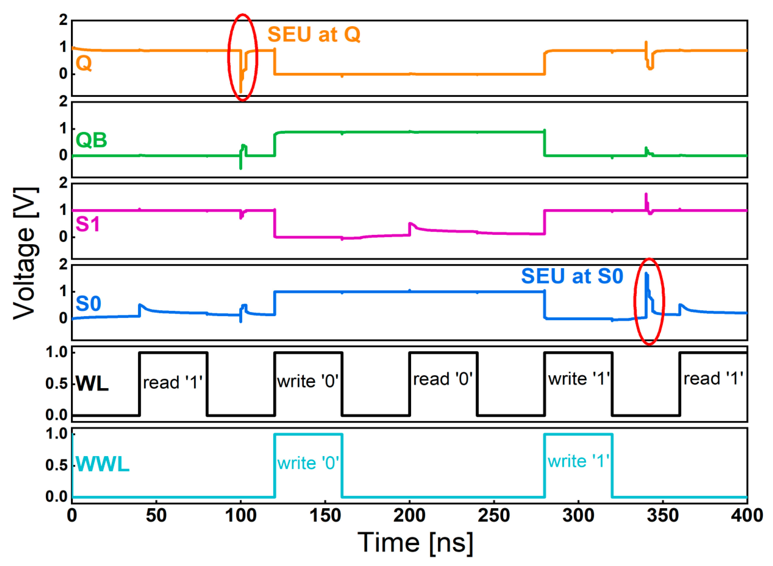
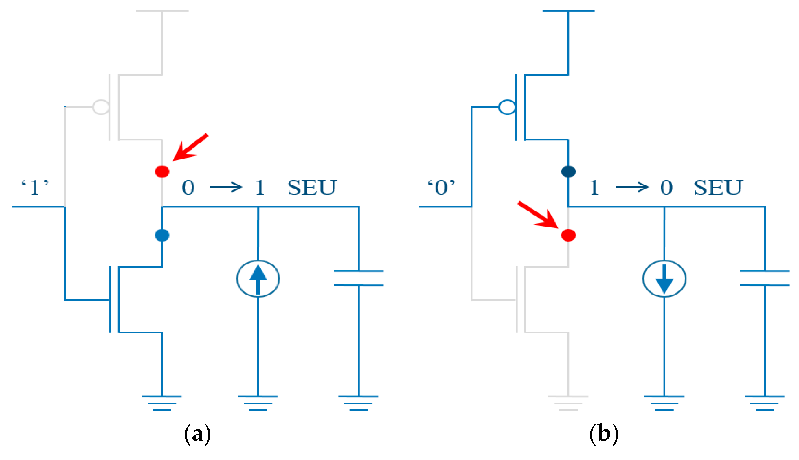
2.2. Soft-Error Recovery Analysis

Transient recovery waveforms and operating behavior of the LDRH16T cell are illustrated in Figure 4. When a high-energy particle strikes the drain region of a reverse-biased OFF-state transistor, excess carriers are generated within the device, producing a transient current pulse at the drain [5]. A node located near the reverse-biased drain diffusion region is considered a sensitive node [17]. Generally, when a radiation particle impacts a PMOS transistor, only a positive transient—such as a ‘1’ → ‘1’ or ‘0’ → ‘1’ transition—can occur, depending on the node’s initial logic level. In contrast, for NMOS transistors, only negative transients such as ‘1’ → ‘0’ or ‘0’ → ‘0’ are possible. Therefore, when the LDRH16T stores logic ‘1’, the storage node QB holds ‘0’ and is surrounded solely by NMOS transistors, making the only possible upset a non-inverting ‘0’ → ‘0’ transition. Similarly, the internal node S1 holds ‘1’ and is connected only to PMOS drains, so it can only undergo a non-inverting ‘1’ → ‘1’ transition during an SEU event. As a result, both QB and S1 can be regarded as insensitive nodes [21]. In hold mode, the proposed memory cell has only two sensitive nodes: Q and S0.
(1) SEU at node Q: When an SEU inverts the stored logic value at node Q from ‘1’ to ‘0’, transistor P5 turns ON, while transistors N2 and N4 turn OFF. Although P5 becomes active, transistors N3 and N1 remain OFF due to the logic level at node QB, thereby maintaining the logic state of node S1. Moreover, since transistor P2 is designed to be stronger than P5, S1 is held even more firmly at its original logic level. As a result, transistors P1, P4, and N6 remain OFF, allowing S0 and QB to retain their respective values. Consequently, transistors P2, P3, and N5 remain ON, while N1 stays OFF, enabling node Q to recover its original logic ‘1’ state.
(2) SEU at node S0: When an SEU causes the internal node S0 to flip from its initial value ‘0’ to ‘1’, transistor N6 turns ON, while transistors P2 and P3 turn OFF. Since P2, P3, and N1 (the latter being OFF due to the hold mode) are all inactive, nodes S1 and Q enter a high-impedance state. In this state, both pull-up and pull-down paths are disconnected, preventing any change in their logic levels. Meanwhile, node QB remains at logic ‘0’ because transistor N2 stays ON, controlled by the logic level at node Q, thereby pulling QB down to GND. Since nodes Q, QB, and S1 are unaffected by the SEU and remain in their original states, node S0 is eventually pulled down to GND through transistors N2, N4, and P6, restoring its initial logic ‘0’ state.
(3) SEMNU at node Q and S0: When a SEMNU occurs, the initial logic values at nodes Q and S0—‘1’ and ‘0’, respectively—are flipped to ‘0’ and ‘1’. As both nodes transition simultaneously, each loses its recovery mechanism, resulting in a permanent logic inversion. However, this type of charge-sharing-induced SEMNU can only occur when the distance between two PMOS transistors is less than 1.62 μm or when the distance between a PMOS and an NMOS transistor is less than 0.6 μm [4]. Therefore, ensuring sufficient spacing between transistors further enhances immunity to SEMNU. As shown in Figure 2, the layout of the proposed LDRH16T cell ensures a physical separation of 6.378 μm between nodes Q and S0, thereby preventing SEMNU from occurring between this sensitive node pair [19].

3. Simulation Results and Analysis

All performance metrics were evaluated based on a 90 nm CMOS technology and a 1 V supply voltage. To demonstrate the effectiveness of the proposed design, its cell-level performance is compared against several contemporary radiation-hardened SRAM cells, including RHBD10T, SIS10T, WE-QUATRO, QUCCE12T, EDP12T, SEA14T, and SAW16T. Key metrics—including read and write access time, read static noise margin, word line write trip voltage, and hold power consumption—were analyzed and compared.

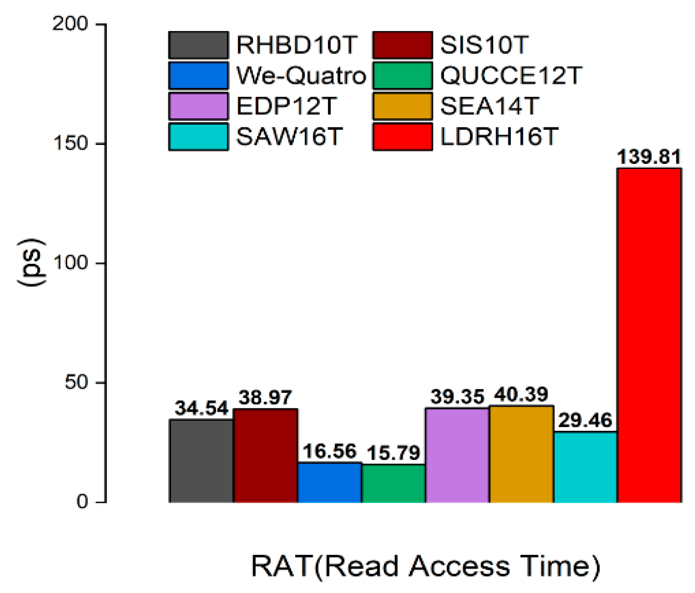
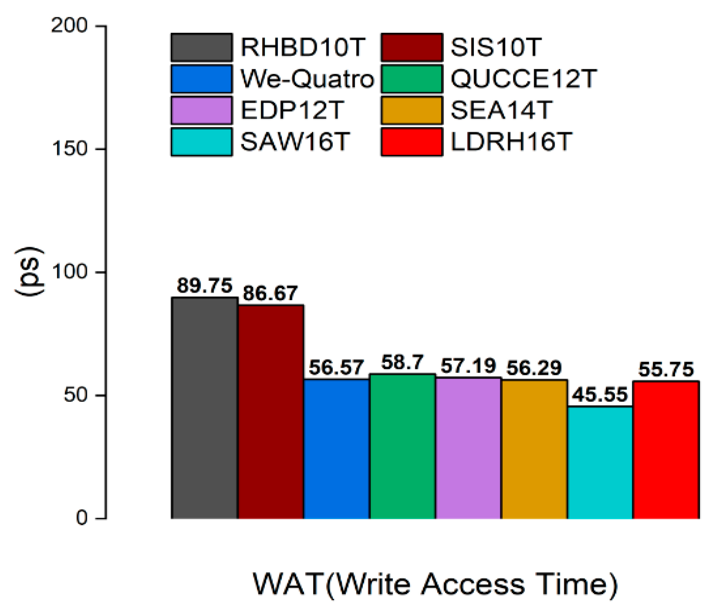
3.1. Read and Write Access Time Comparison

Read access time (RAT) is defined as the time interval between the point at which the word line (WL) reaches 50% of the supply voltage (VDD) and the moment a voltage difference of 50 mV develops between the bit lines BL and BLB [22]. During the read operation, the voltage at the node storing logic ‘0’ may rise due to a voltage division effect between the access transistor and the pull-down path. This voltage rise reduces the drive strength of the access transistor due to the body effect, thereby increasing the RAT. Consequently, a higher cell ratio (CR) generally results in a shorter read access time. Additionally, excessive use of access transistors increases bit line capacitance compared to designs using a single access transistor, thereby lengthening the RAT. On the other hand, having additional read paths can help reduce the RAT. As shown in Figure 5, the proposed LDRH16T cell exhibits the longest read access time among the compared designs. Despite having a cell ratio of 2.5, only the access transistors connected to the internal nodes are activated during the read operation, leading to higher bit line capacitance than in cells with a single access transistor. Furthermore, LDRH16T includes a PMOS device in the read discharge path and only one effective discharge path, which further increases the RAT [9]. Lastly, excessive transistor stacking in the pull-down path causes the voltage at the ‘0’-storing internal node to rise, resulting in the longest RAT among all evaluated cells.
Write access time (WAT) is evaluated as the time interval between the point at which the WL reaches 50% of VDD and the moment the voltages of storage nodes Q and QB intersect [9]. It is generally observed that applying simultaneous influence to both the storage and internal nodes during a write operation leads to a reduction in write access time (WAT). According to Figure 6, LDRH16T achieves the second fastest WAT among the compared designs. Since the proposed cell includes two additional access transistors connected to the internal nodes, both the internal and storage nodes are flipped simultaneously during a write operation, reducing the overall WAT. As a result, the LDRH16T outperforms RHBD10T, SIS10T, EDP12T, and SEA14T, which rely on only one access transistor. Moreover, in both LDRH16T and SAW16T, the logic ‘1’ is stored through an NMOS pull-up path, which creates a weaker ‘1’. This makes it easier to discharge during a write operation, thereby reducing the WAT due to a smaller voltage swing between nodes. Among all designs, SAW16T exhibits the shortest WAT. This is attributed to its positive feedback structure formed by the pull-down transistors, where the change in one storage node accelerates the change in the complementary node, resulting in faster write completion. Additionally, LDRH16T uses separate WL and WWL signals to control its two pairs of access transistors. This separation may introduce timing mismatch during the write operation, potentially delaying the initiation of write feedback [9]. In contrast, SAW16T controls both pairs of access transistors using a single WL signal, enabling more synchronized activation and thereby achieving a faster WAT.

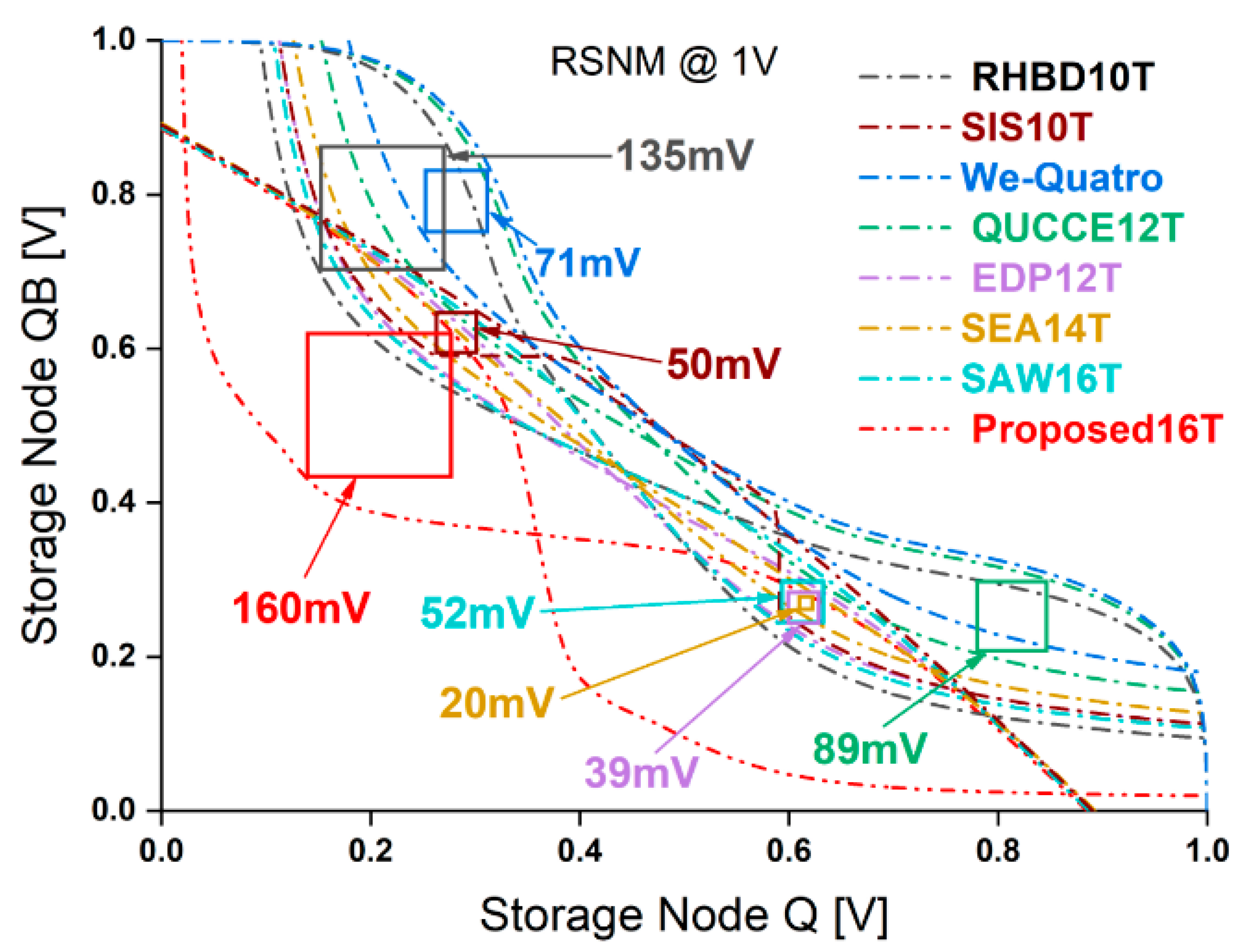
3.2. Read Stability Comparison

One of the major drawbacks of the conventional 6T SRAM cell is its vulnerability to reading instability. During a read operation, the storage node holding logic ‘0’ is directly connected to the pre-charged bit line at VDD, allowing a read current to flow. This current may cause a voltage rise at the ‘0’-storing node, potentially flipping the stored data. As the voltage increases, the noise margin of the cell decreases, reducing its tolerance to disturbances. Therefore, ensuring read stability is essential for reliable SRAM functionality. Read stability is typically evaluated using the read static noise margin (RSNM), which is measured by applying a DC voltage sweep to the storage nodes and generating the butterfly curve through DC analysis [22]. The RSNM is quantified as the side length of the largest square that can fit within the lobes of the butterfly curve. Figure 7 illustrates the butterfly curves of all compared cells. Among the designs, SIS10T, EDP12T, and SEA14T exhibit relatively low RSNM values due to their weak pull-up or pull-down strength at the storage nodes. In addition, WE-QUATRO, QUCCE12T, and SAW16T are susceptible to read upsets because two access transistors are positioned near each bit line, exposing not only the storage nodes but also the internal nodes to potential bit line noise. RHBD10T, which has the highest cell ratio (CR = 3), shows improved RSNM performance by keeping the voltage of the ‘0’-storing node relatively low during a read operation. As a result, it achieves higher RSNM than all comparison cells except for the proposed LDRH16T. As shown in Figure 7, the LDRH16T cell exhibits the highest RSNM among all evaluated designs. This is mainly attributed to its read-decoupled architecture, in which only WL is activated during a read, while WWL remains OFF [1,20]. This ensures that only the internal nodes are connected to the bit lines through a single pair of access transistors, while the storage nodes Q and QB remain completely isolated. Therefore, even if the voltage of the internal node increases to a level that could flip its state, it does not affect the stored data at Q and QB. This read-decoupled technique is a structural-level approach that is inherently independent of process technology, enabling its applicability across various technology nodes. Furthermore, the proposed cell is designed with a relatively high cell ratio (CR = 2.5), which lowers the voltage at the ‘0’-storing internal node S0, further enhancing read stability. Consequently, the LDRH16T achieves the highest RSNM among the compared designs, ensuring robust read operation under radiation-prone conditions.

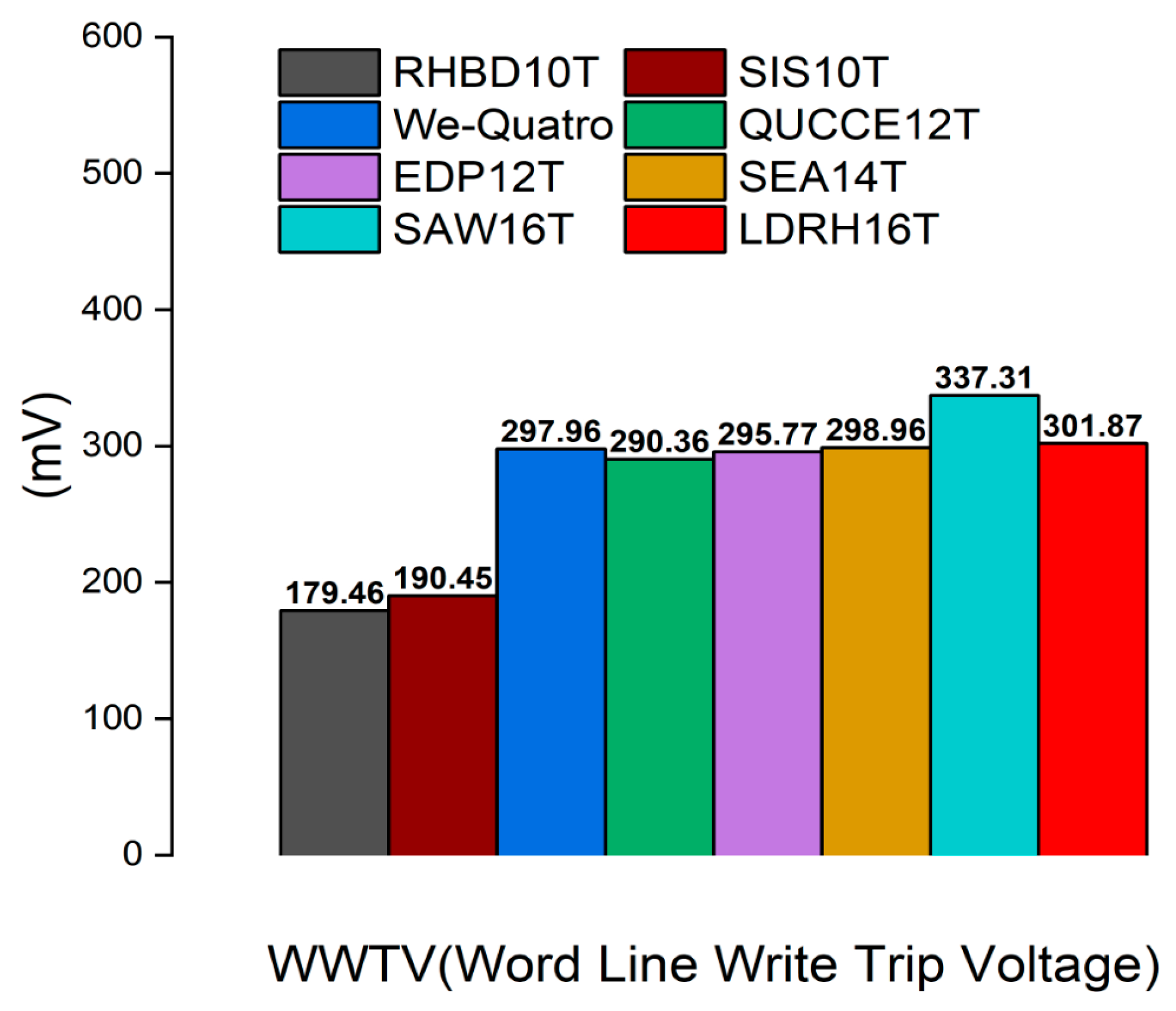
3.3. Write Ability Comparison

The write static noise margin (WSNM) has been used as a design metric to evaluate the write ability of SRAM cells. However, recent studies suggest that a more reliable indicator of write capability is the word line write trip voltage (WWTV) [9]. To measure WWTV, a write simulation is performed by supplying the desired data to the bit lines. WWTV is defined as the voltage difference between VDD and WL at the point where the storage nodes Q and QB intersect during a write operation. Cells with longer write access times (WAT) require more time to flip the stored data, which causes Q and QB to intersect at a higher WL voltage level—resulting in a lower WWTV. Therefore, there is an inverse relationship between WWTV and WAT across different cells. As a result, the ranking of cells based on WWTV (Figure 8) exactly mirrors the inverse of their WAT (Figure 6) ranking. According to the simulation results, the proposed LDRH16T cell achieves a higher WWTV than all other comparison cells except for SAW16T. This indicates that the LDRH16T offers strong write capability while maintaining radiation-hardened features.

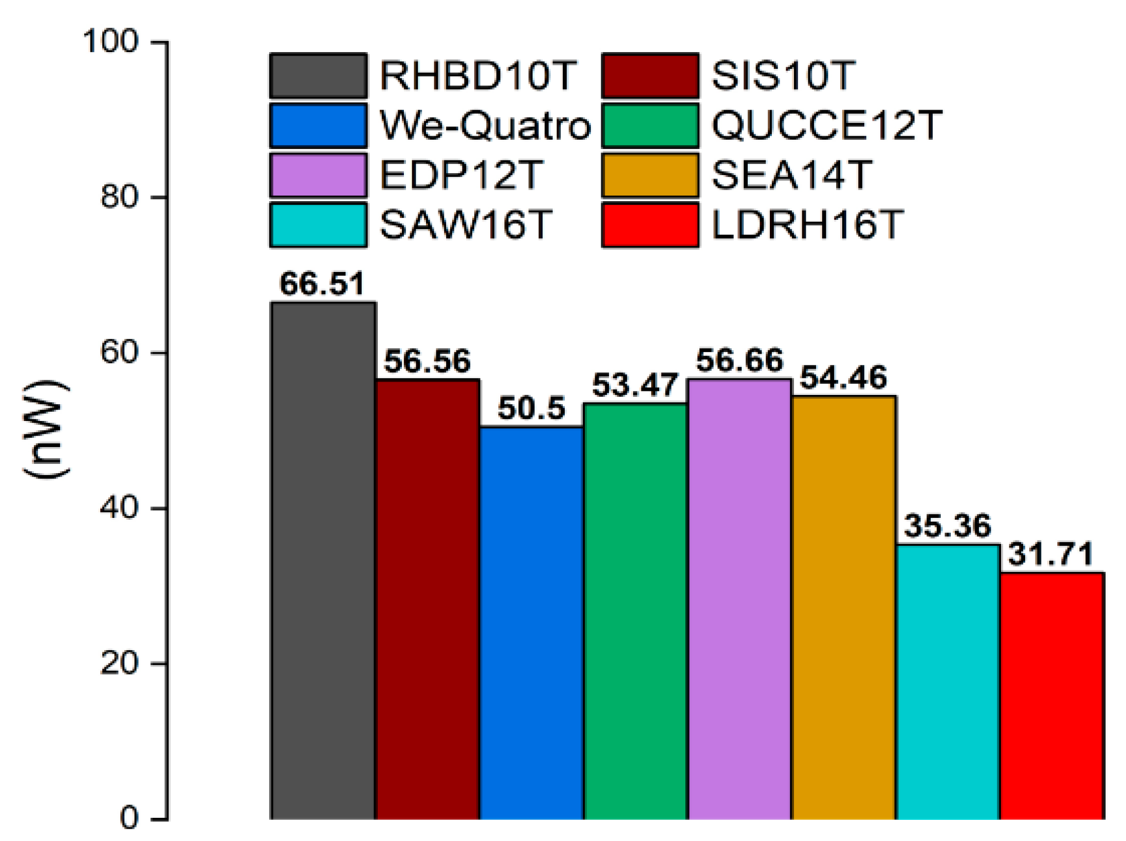
3.4. Hold Power Comparison

Since SRAM cells remain in hold mode for most of their operation, the power consumed during this mode significantly impacts the total power consumption of the cell. Therefore, minimizing leakage power in the hold state plays a crucial role in reducing the overall power consumption of the cell. Hold power (HPWR) refers to the power consumed when an SRAM cell is in hold mode and is typically measured by applying a pulse from 0 to VDD to all nodes storing logic ‘1’ and recording the power when the voltage reaches VDD. HPWR is primarily consumed due to bit line leakage and leakage within the inverter structure. In the bit line, NMOS transistors generally show higher HPWR than PMOS transistors because of their higher carrier mobility. Additionally, when there are more current paths from VDD to ground inside the cell, HPWR tends to be higher. If the resistance of the pull-up and pull-down paths in the inverters is high, the leakage power generated within the inverter structure can be reduced. A comparison of HPWR across all evaluated cells is illustrated in Figure 9. Among them, SAW16T and LDRH16T exhibit lower HPWR than all other reference cells. Despite having four NMOS access transistors, both cells include transistor stacking internally and only two NMOS transistors connected to ground, which helps reduce leakage [9,23]. Additionally, LDRH16T connects only two PMOS transistors to VDD, thereby supplying less current from VDD and resulting in the lowest HPWR among all comparison cells [21].

3.5. Verification and Comparison of Soft-Error Robustness

To verify the soft-error recovery capability of the proposed cell, a double exponential current source is used to simulate a single-event upset (SEU). By choosing the appropriate direction of the current source, a positive transient pulse is generated at the drain of an OFF-state PMOS, and a negative transient pulse is generated at the drain of an OFF-state NMOS. Therefore, to evaluate soft-error immunity, a negative transient pulse is injected into the Q node storing logic ‘1’, and a positive transient pulse is injected into the S0 node storing logic ‘0’ (see Figure 10). The injected current is defined as follows [22]:
I ( t ) = I O e t τ α e t τ β
I O = Q τ α τ β
Here, IO is the peak current of the pulse, Q is the total collected charge, τα is the junction collection time constant, and τβ is the initial ion track establishment time constant. In this study, τα is set to 200 ps and τβ to 50 ps for computational simplicity [4,20]. The critical charge (QC) is defined as the minimum amount of charge required to flip the stored data when a sensitive node is affected by an SEU. Soft-error immunity is evaluated by measuring QC for all sensitive nodes in the SRAM cell, and the lowest value is considered the effective QC of the cell. The effective QC values of all cells are measured and compared accordingly. The measured effective QC values are listed in Table 1. Figure 11 shows the simulated waveforms of the proposed cell when varying charges from 30 fC to 150 fC are injected into nodes Q and S0. Since LDRH16T has only two sensitive nodes when storing logic ‘1’, only Q and S0 are used for SEU validation. Importantly, the proposed cell can autonomously recover to its original state even when exposed to SEUs with charge levels exceeding 150 fC. This is because all transistors are part of a sufficiently strong feedback structure, which allows the cell to promptly restore the original data even after it has been disturbed. All other comparison cells except for EDP12T and SEA14T have finite QC values due to partial SEU immunity. Furthermore, as described in Section 2, the layout of LDRH16T ensures sufficient spacing between nodes Q and S0, thereby preventing charge sharing between these sensitive nodes. Therefore, the proposed cell is highly suitable for operation in radiation-prone environments.

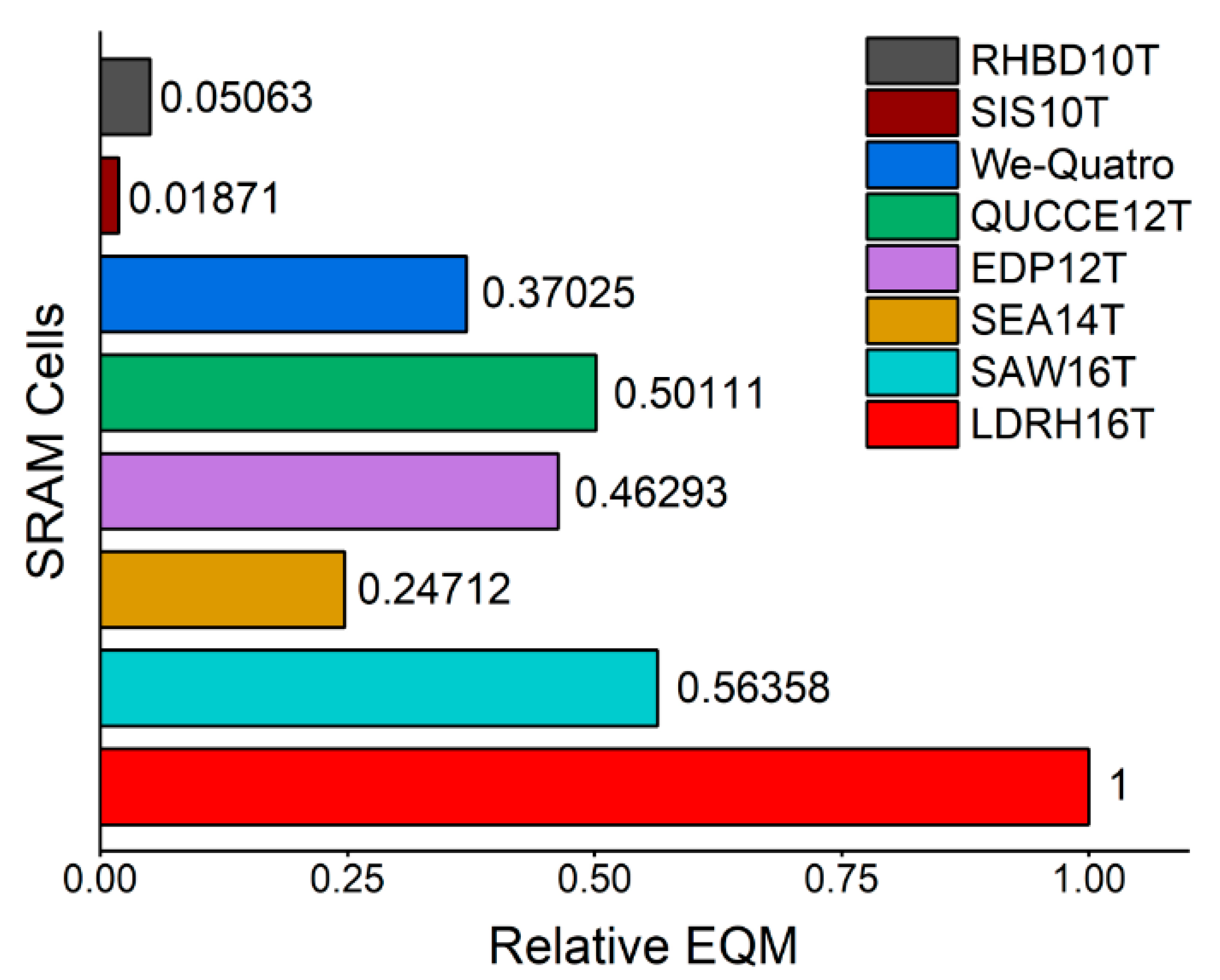
3.6. Electric Quality Metric Comparison

Many of the design metrics for radiation-hardened SRAMs exhibit trade-off relationships. For example, increasing the supply voltage (VDD) can improve critical charge, RSNM, WWTV, RAT, and WAT, but it also increases HPWR. In addition, the proposed LDRH16T cell demonstrates strong performance in terms of read stability and leakage power, but it has a slight drawback in read access time. To account for these factors, we propose an electrical quality metric (EQM) for evaluating the overall performance of SRAM cells. The formula for this metric is defined as follows [17,24]:
E Q M = Q C × R S N M × W W T V H P W R × R A T × W A T
A cell with a higher EQM is considered to exhibit better overall performance. Figure 12 presents the EQM values of the proposed LDRH16T cell and all other comparison cells. As shown in the graph, the LDRH16T achieves the highest EQM value among all designs. This result confirms that the proposed cell offers superior overall performance.

4. Conclusions

This paper presented a low-power, read-decoupled, radiation-hardened 16T (LDRH16T) SRAM cell for aerospace applications. The proposed design achieves full recovery from single-event upset (SEU) injected at all sensitive nodes, as validated through dual-current pulse simulations. Notably, the proposed cell is capable of recovering from SEUs with injected charges exceeding 150 fC at all sensitive nodes. In addition, the LDRH16T cell features fewer sensitive nodes than most reference designs, inherently reducing the probability of SEU occurrence. Its layout is optimized to enhance resilience against single-event multi-node upsets (SEMNU) by minimizing charge-sharing effects between adjacent nodes. Beyond its radiation tolerance, the proposed cell exhibits the highest read static noise margin (RSNM) of 160 mV, representing improvements of 1.19×, 3.20×, 2.25×, 1.80×, 4.10×, 8.00×, and 3.08× compared to RHBD10T, SIS10T, WE-QUATRO, QUCCE12T, EDP12T, SEA14T, and SAW16T, respectively. In addition, the hold power consumption (HPWR) of the proposed cell is 31.71 nW, which is 0.48×, 0.56×, 0.63×, 0.59×, 0.56×, 0.58×, and 0.90× lower than that of the same reference cells, respectively. The write performance, measured in terms of word line write trip voltage (WWTV), is 301.87 mV, showing improvements of 1.68×, 1.59×, 1.01×, 1.04×, 1.02×, and 1.01× over all comparison cells except SAW16T. Although the LDRH16T exhibits slightly longer read access time, it delivers the highest overall performance as measured by the electrical quality metric (EQM). Future work should consider incorporating design improvements aimed at reducing the read access time. These results indicate that LDRH16T is a highly promising solution for aerospace systems requiring long-term data reliability with minimal power consumption.

Author Contributions

Conceptualization, S.-J.L. and S.-H.J.; methodology, S.-J.L.; validation, S.-J.L.; data curation, S.-J.L.; writing—original draft preparation, S.-J.L.; writing—review and editing, S.-H.J.; visualization, S.-J.L.; supervision, S.-H.J.; project administration, S.-H.J. All authors have read and agreed to the published version of the manuscript.

Funding

This research received no external funding.

Institutional Review Board Statement

Not applicable.

Informed Consent Statement

Not applicable.

Data Availability Statement

The original contributions presented in this study are included in the article. Further inquiries can be directed to the corresponding author.

Acknowledgments

The EDA Tool was supported by the IC Design Education Center, Republic of Korea.

Conflicts of Interest

The authors declare no conflicts of interest.

References

  1. Pal, S.; Sri, D.D.; Ki, W.-H.; Islam, A. Soft-Error Resilient Read Decoupled SRAM with Multi-Node Upset Recovery for Space Applications. IEEE Trans. Electron Devices 2021, 68, 2246–2254. [Google Scholar] [CrossRef]
  2. Apollos, E.C. Design Principles of SRAM Memory in Nano-CMOS Technologies. Int. J. Comput. Appl. 2019, 178, 5–11. [Google Scholar]
  3. De Caro, D.; Di Meo, G.; Napoli, E.; Petra, N.; Strollo, A.G.M. A 1.45 GHz All-Digital Spread Spectrum Clock Generator in 65nm CMOS for Synchronization-Free SoC Applications. IEEE Trans. Circuits Syst. I 2020, 67, 3839–3852. [Google Scholar] [CrossRef]
  4. Bai, N.; Xiao, X.; Xu, Y.; Wang, Y.; Wang, L.; Zhou, X. Soft-Error-Aware Sram with Multinode Upset Tolerance for Aerospace Applications. IEEE Trans. Very Large Scale Integr. (VLSI) Syst. 2023, 32, 128–136. [Google Scholar] [CrossRef]
  5. Amusan, O.A.; Witulski, A.F.; Massengill, L.W.; Bhuva, B.L.; Fleming, P.R.; Alles, M.L.; Sternberg, A.L.; Black, J.D.; Schrimpf, R.D. Charge Collection and Charge Sharing in a 130 Nm CMOS Technology. IEEE Trans. Nucl. Sci. 2006, 53, 3253–3258. [Google Scholar] [CrossRef]
  6. Chen, Z.; Zhang, M.; Han, W. Design of SEU Tolerant 2D-FFT in SRAM-Based FPGA. In Proceedings of the 2021 IEEE 3rd International Conference on Circuits and Systems (ICCS), Chengdu, China, 29–31 October 2021; IEEE: Piscataway, NJ, USA, 2021; pp. 88–93. [Google Scholar]
  7. Bajura, M.A.; Boulghassoul, Y.; Naseer, R.; DasGupta, S.; Witulski, A.F.; Sondeen, J.; Stansberry, S.D.; Draper, J.; Massengill, L.W.; Damoulakis, J.N. Models and Algorithmic Limits for an ECC-Based Approach to Hardening Sub-100-Nm SRAMs. IEEE Trans. Nucl. Sci. 2007, 54, 935–945. [Google Scholar] [CrossRef]
  8. Lyons, R.E.; Vanderkulk, W. The Use of Triple-Modular Redundancy to Improve Computer Reliability. IBM J. Res. Dev. 1962, 6, 200–209. [Google Scholar] [CrossRef]
  9. Pal, S.; Ki, W.-H.; Tsui, C.-Y. Soft-Error-Aware Read-Stability-Enhanced Low-Power 12T SRAM with Multi-Node Upset Recoverability for Aerospace Applications. IEEE Trans. Circuits Syst. I Regul. Pap. 2022, 69, 1560–1570. [Google Scholar] [CrossRef]
  10. Jahinuzzaman, S.M.; Rennie, D.J.; Sachdev, M. A Soft Error Tolerant 10T SRAM Bit-Cell with Differential Read Capability. IEEE Trans. Nucl. Sci. 2009, 56, 3768–3773. [Google Scholar] [CrossRef]
  11. Kim, J.S.; Chang, I.J. We-Quatro: Radiation-Hardened SRAM Cell with Parametric Process Variation Tolerance. IEEE Trans. Nucl. Sci. 2017, 64, 2489–2496. [Google Scholar]
  12. Jiang, J.; Xu, Y.; Zhu, W.; Xiao, J.; Zou, S. Quadruple Cross-Coupled Latch-Based 10T and 12T SRAM Bit-Cell Designs for Highly Reliable Terrestrial Applications. IEEE Trans. Circuits Syst. I Regul. Pap. 2018, 66, 967–977. [Google Scholar] [CrossRef]
  13. Dohar, S.S.; Siddharth, R.K.; Vasantha, M.H.; YB, N.K. A 1.2 V, Highly Reliable RHBD 10T SRAM Cell for Aerospace Application. IEEE Trans. Electron Devices 2021, 68, 2265–2270. [Google Scholar] [CrossRef]
  14. Pal, S.; Sahay, S.; Ki, W.-H.; Tsui, C.-Y. A 10T Soft-Error-Immune SRAM with Multi-Node Upset Recovery for Low-Power Space Applications. IEEE Trans. Device Mater. Reliab. 2022, 22, 85–88. [Google Scholar] [CrossRef]
  15. Pal, S.; Mohapatra, S.; Ki, W.-H.; Islam, A. Design of Soft-Error-Aware SRAM with Multi-Node Upset Recovery for Aerospace Applications. IEEE Trans. Circuits Syst. I Regul. Pap. 2021, 68, 2470–2480. [Google Scholar] [CrossRef]
  16. Pal, S.; Chowdary, G.; Ki, W.-H.; Tsui, C.-Y. Energy-Efficient Dual-Node-Upset-Recoverable 12T SRAM for Low-Power Aerospace Applications. IEEE Access 2022, 11, 20184–20195. [Google Scholar] [CrossRef]
  17. Bai, N.; Zhao, W.; Xu, Y.; Wang, Y. A Low-Energy Critical Charge-Enhanced SRAM for Aerospace Applications. In Proceedings of the 2024 IEEE International Test Conference in Asia (ITC-Asia), Changsha, China, 18-20 August 2024; IEEE: Piscataway, NJ, USA, 2024; pp. 1–6. [Google Scholar]
  18. Oh, J.-Y.; Jo, S.-H. Radiation-Hardened 16T SRAM Cell with Improved Read and Write Stability for Space Applications. Appl. Sci. 2024, 14, 11940. [Google Scholar] [CrossRef]
  19. Qi, C.; Xiao, L.; Wang, T.; Li, J.; Li, L. A Highly Reliable Memory Cell Design Combined with Layout-Level Approach to Tolerant Single-Event Upsets. IEEE Trans. Device Mater. Reliab. 2016, 16, 388–395. [Google Scholar] [CrossRef]
  20. Pal, S.; Mohapatra, S.; Ki, W.-H.; Islam, A. Soft-Error-Aware Read-Decoupled SRAM with Multi-Node Recovery for Aerospace Applications. IEEE Trans. Circuits Syst. II Express Briefs 2021, 68, 3336–3340. [Google Scholar] [CrossRef]
  21. Naz, S.F.; Mondal, D.; Shah, A.P. Side-Channel Attack Resilient RHBD 12T SRAM Cell for Secure Nuclear Environment. IEEE Trans. Device Mater. Reliab. 2023, 24, 59–67. [Google Scholar] [CrossRef]
  22. Pal, S.; Mohapatra, S.; Ki, W.-H.; Islam, A. Soft-Error-Immune Read-Stability-Improved SRAM for Multi-Node Upset Tolerance in Space Applications. IEEE Trans. Circuits Syst. I Regul. Pap. 2021, 68, 3317–3327. [Google Scholar] [CrossRef]
  23. Chetan, P.C.; Dahiya, P.K. Different Leakage Power Reduction Techniques in SRAM Circuits: A State-of-the-Art Review. Int. Res. J. Eng. Technol. 2017, 4, 742–745. [Google Scholar]
  24. Mukku, P.K.; Lorenzo, R. A Soft Error Upset Recovery SRAM Cell for Aerospace and Military Applications. In Proceedings of the TENCON 2023—2023 IEEE Region 10 Conference (TENCON), Chiang Mai, Thailand, 31 October–3 November 2023; IEEE: Piscataway, NJ, USA, 2023; pp. 744–749. [Google Scholar]
Figure 1. Schematic of the proposed LDRH16T cell.
Applsci 15 06536 g001
Figure 2. The layout of the proposed LDRH16T cell.
Applsci 15 06536 g002
Figure 3. Operation of the proposed LDRH16T cell.
Applsci 15 06536 g003
Figure 4. SEU resilience verification waveform of the proposed LDRH16T cell.
Applsci 15 06536 g004
Figure 5. Comparison of RAT between the proposed LDRH16T and previous works.
Applsci 15 06536 g005
Figure 6. Comparison of WAT between the proposed LDRH16T and previous works.
Applsci 15 06536 g006
Figure 7. Comparison of RSNM between the proposed LDRH16T and previous works.
Applsci 15 06536 g007
Figure 8. Comparison of WWTV between the proposed LDRH16T and previous works.
Applsci 15 06536 g008
Figure 9. Comparison of HPWR between the proposed LDRH16T and previous works.
Applsci 15 06536 g009
Figure 10. Equivalent circuits used to simulate (a) a positive and (b) a negative injected noise.
Applsci 15 06536 g010
Figure 11. Soft-error recovery when an SEU affects (a) node Q and (b) node S0.
Applsci 15 06536 g011
Figure 12. Comparison of relative EQM.
Applsci 15 06536 g012
Table 1. Performance comparison.
StructureQC
(fC)
RAT
(ps)
WAT
(ps)
RSNM
(mV)
WWTV
(mV)
HPWR
(nW)
RHBD10T [13]12.6334.5489.75135179.4666.51
SIS10T [14]1138.9786.6750190.4556.56
We-Quatro [11]24.2716.5656.5771297.9650.5
QUCCE12T [12]28.1715.7958.789290.3653.47
EDP12T [16]>15039.3557.1939295.7756.66
SEA14T [15]>15040.3956.2920298.9654.46
SAW16T [17]44.6929.4645.5552337.3135.36
LDRH16T>150139.8155.75160301.8731.71
Disclaimer/Publisher’s Note: The statements, opinions and data contained in all publications are solely those of the individual author(s) and contributor(s) and not of MDPI and/or the editor(s). MDPI and/or the editor(s) disclaim responsibility for any injury to people or property resulting from any ideas, methods, instructions or products referred to in the content.

