


Numerical Analysis for Cost-Effective Temperature Reduction in High-Power Light-Emitting Diodes Using Thermal via Array

 , and
, and
Abstract
1. Introduction
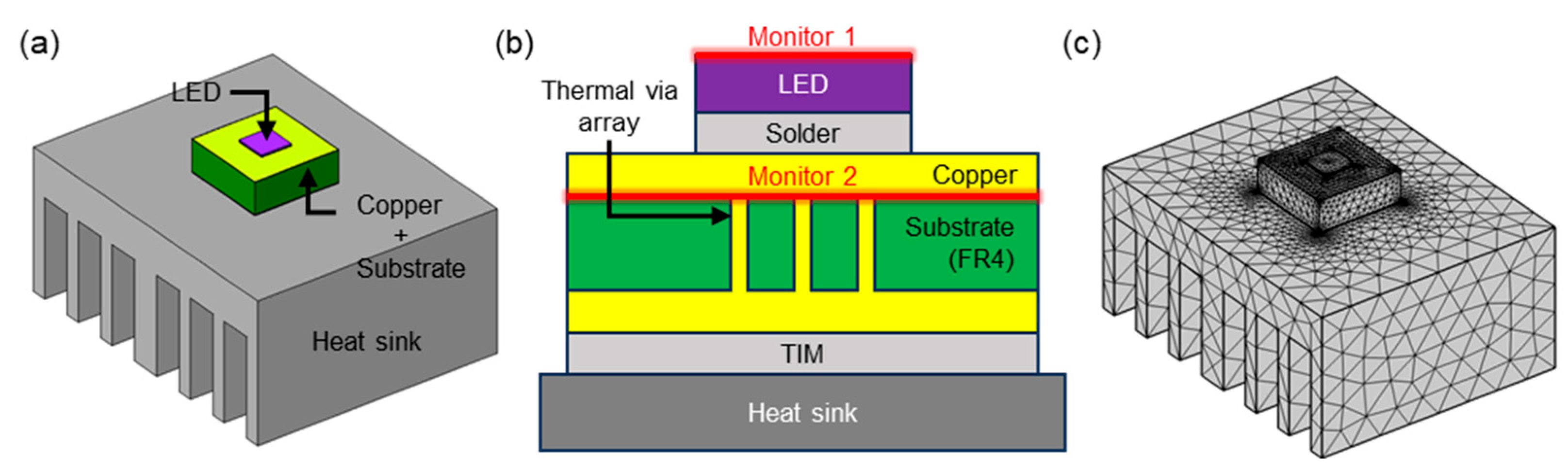
2. Methods
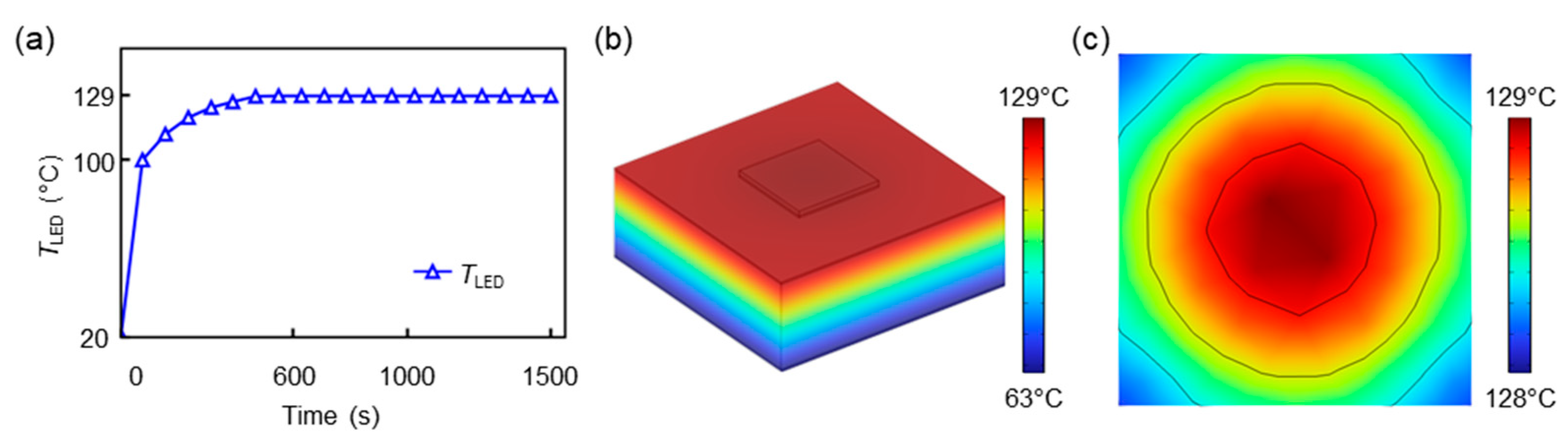
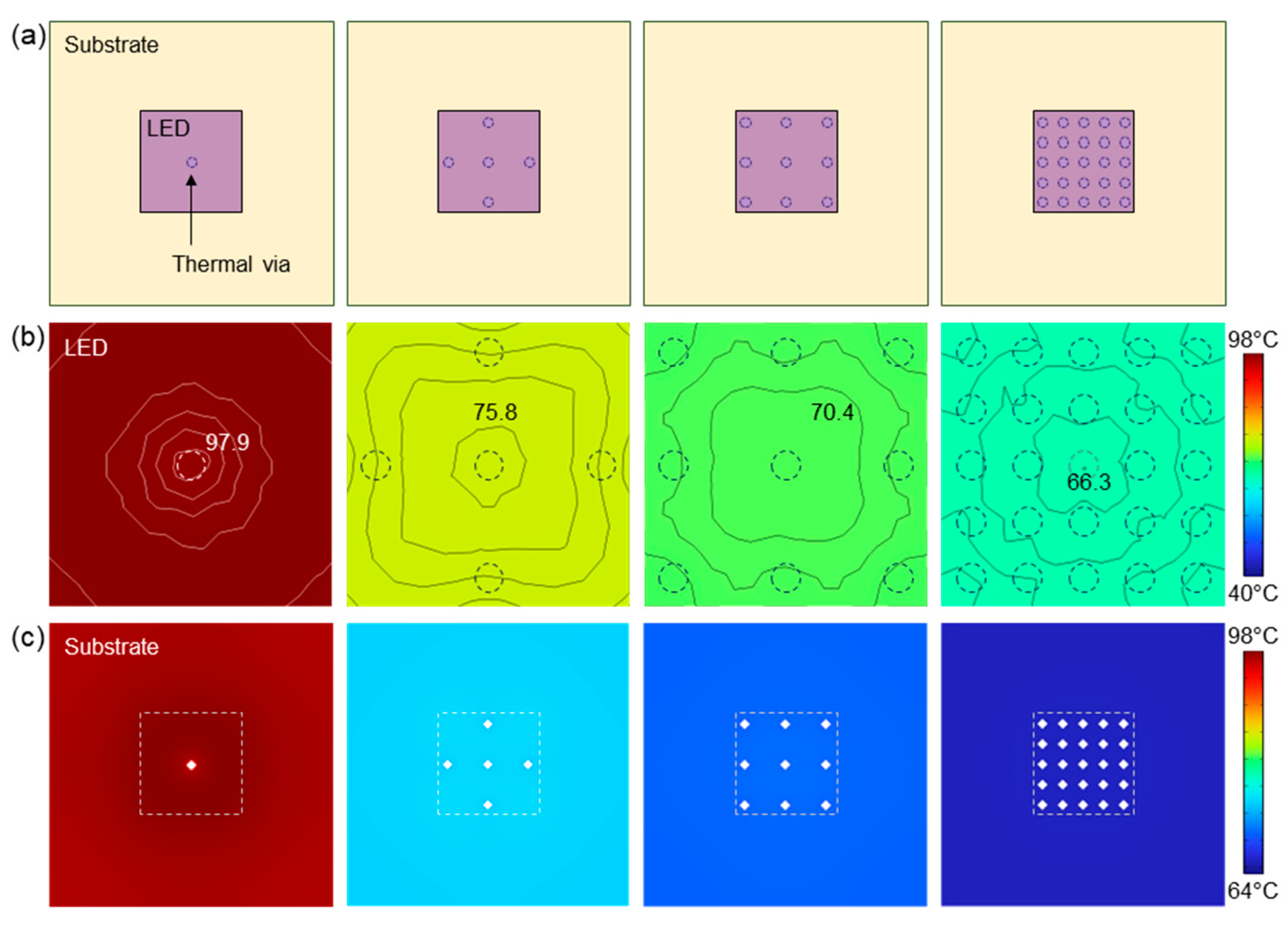
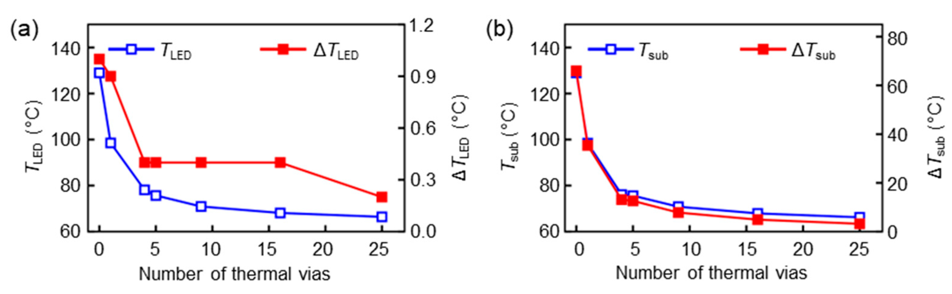
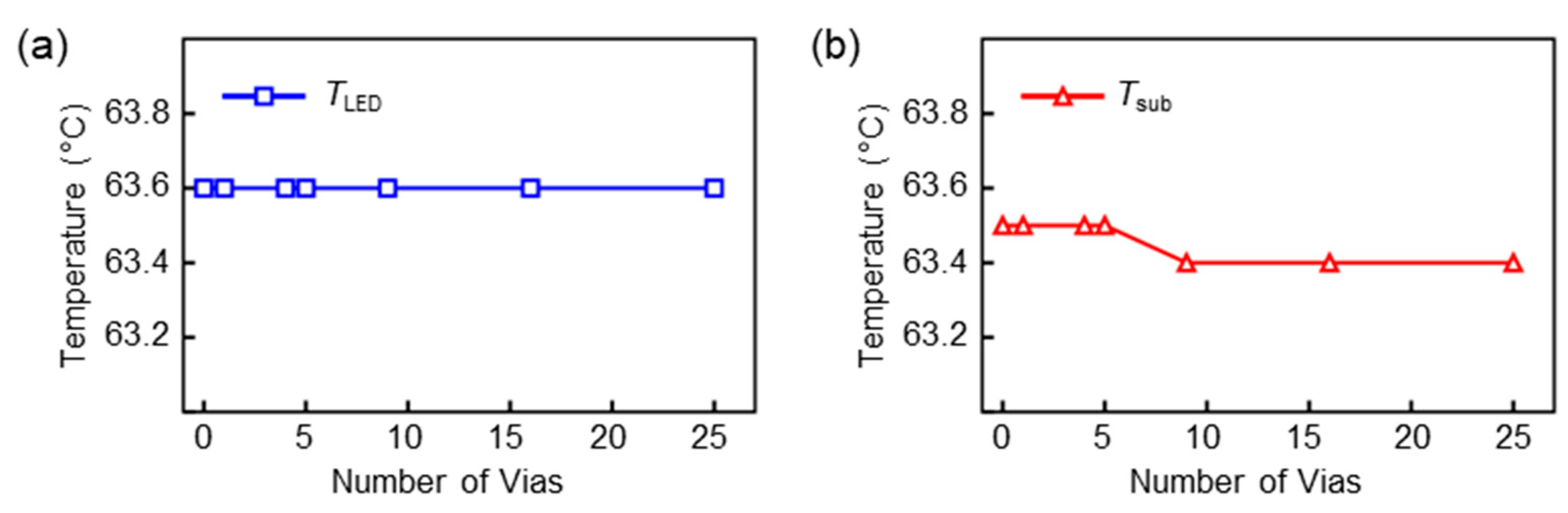
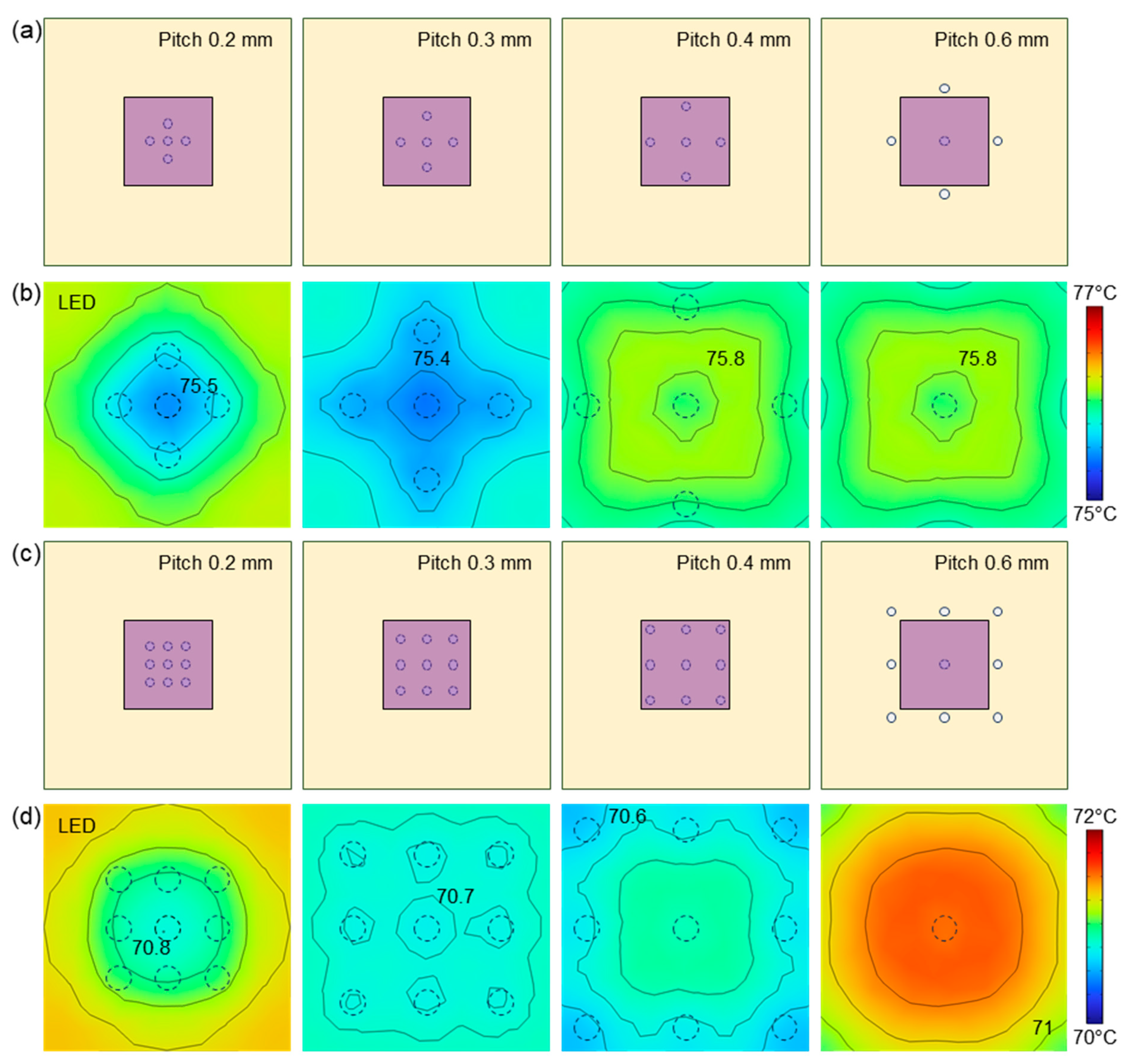
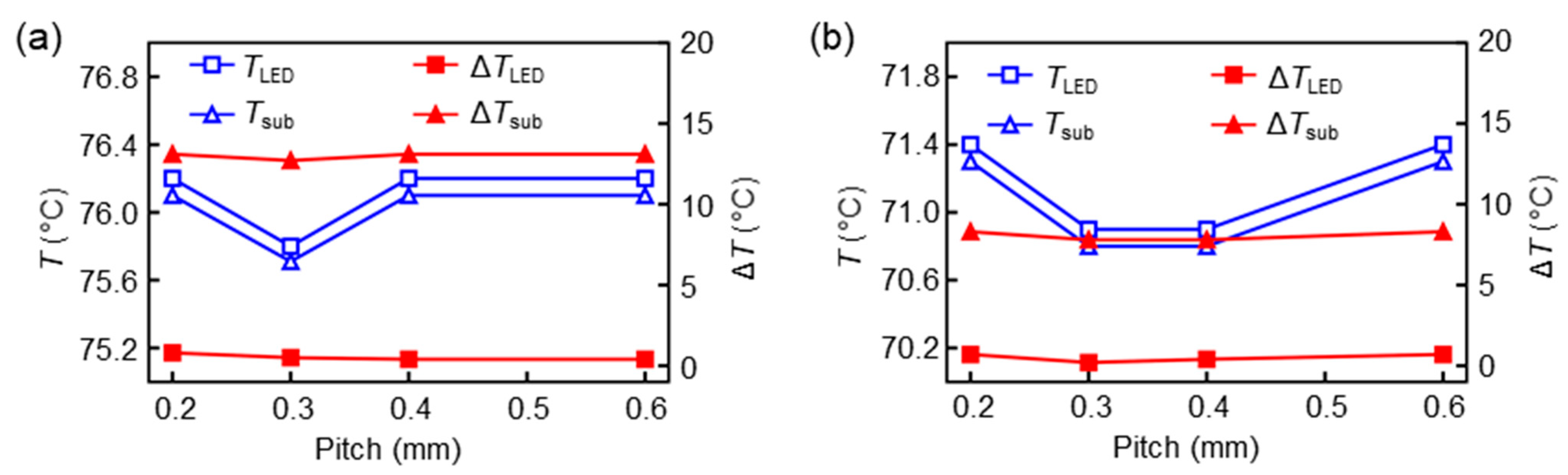
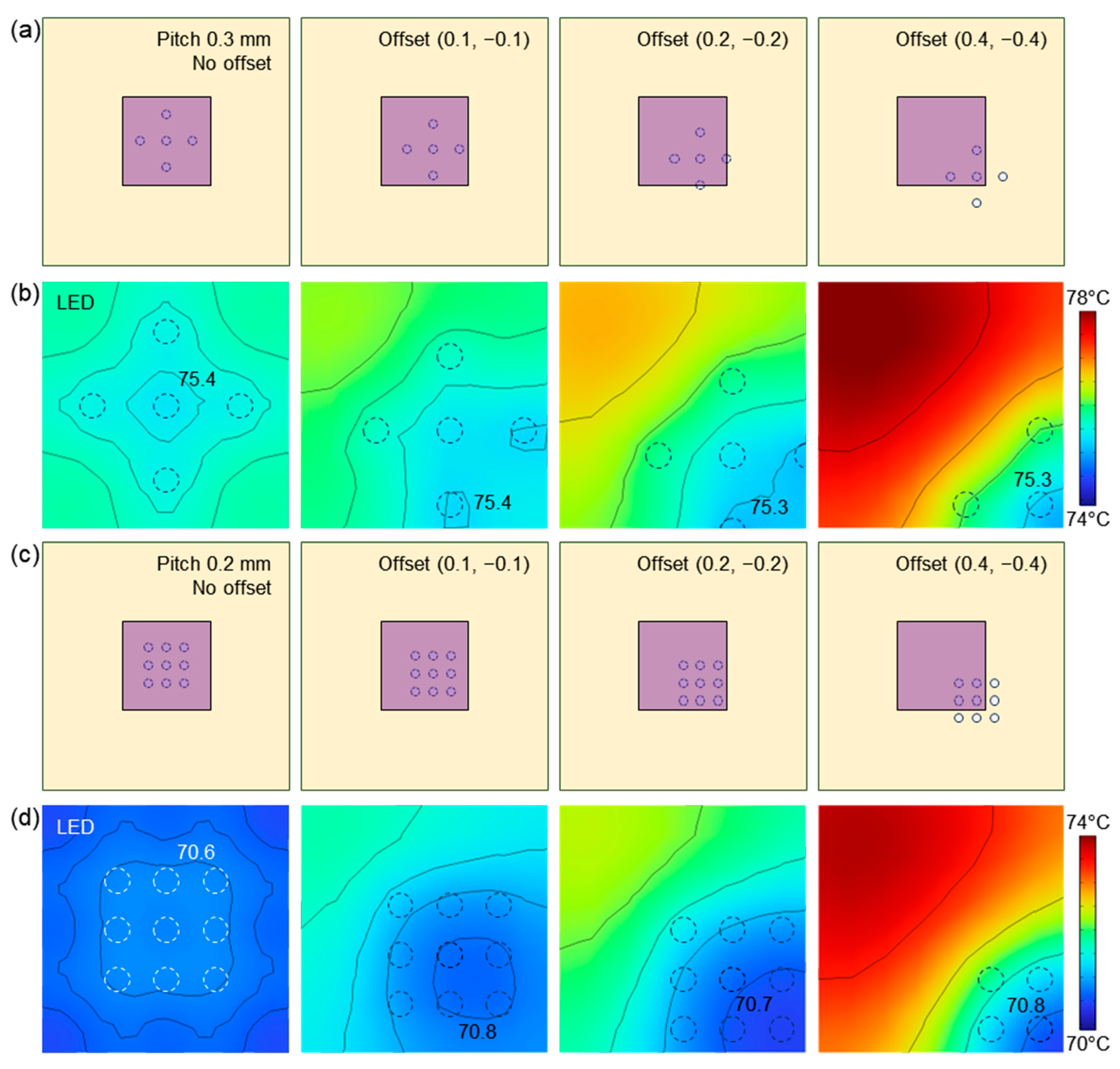
3. Results and Discussion
4. Conclusions
Author Contributions
Funding
Institutional Review Board Statement
Informed Consent Statement
Data Availability Statement
Acknowledgments
Conflicts of Interest
Abbreviations
| LED | Light-emitting diode |
| FEA | Finite element analysis |
References
- Arik, M.; Becker, C.A.; Weaver, S.E.; Petroski, J. Thermal Management of LEDs: Package to System. In Proceedings of the Third International Conference on Solid State Lighting, San Diego, CA, USA, 5–7 August 2003; Volume 5187, p. 64. [Google Scholar]
- Ye, H.; Sau, K.; Van Zeijl, H.; Gielen, A.W.J.; Zhang, G. A Review of Passive Thermal Management of LED Module. J. Semicond. 2011, 32, 014008. [Google Scholar] [CrossRef]
- Tong, X.C. Advanced Materials for Thermal Management of Electronic Packaging; Springer Series in Advanced Microelectronics; Springer: New York, NY, USA, 2011; Volume 30, pp. 233–276. ISBN 9781441977588. [Google Scholar]
- Narendran, N.; Gu, Y. Life of LED-Based White Light Sources. J. Disp. Technol. 2005, 1, 167–171. [Google Scholar] [CrossRef]
- Pan, X.; Wei, M.; Yang, C.; Xiao, H.; Wang, C.; Wang, X. Growth of GaN Film on Si (111) Substrate Using AlN Sandwich Structure as Buffer. J. Cryst. Growth 2011, 318, 464–467. [Google Scholar] [CrossRef]
- Birchmore, S. Book Reviews: Technology Condemned. Expo. Times 1992, 103, 126–127. [Google Scholar] [CrossRef]
- Nam, S.R.; Jung, C.W.; Choi, C.H.; Kang, Y.T. Cooling Performance Enhancement of LED (Light Emitting Diode) Packages with Carbon Nanogrease. Energy 2013, 60, 195–203. [Google Scholar] [CrossRef]
- Kim, C.M.; Kang, Y.T. Cooling Performance Enhancement of LED (Light Emitting Diode) Using Nano-Pastes for Energy Conversion Application. Energy 2014, 76, 468–476. [Google Scholar] [CrossRef]
- Li, H.; Zhu, X.; Zhang, D.; Gao, Y.; Feng, Y.; Ma, Z.; Huang, J.; He, H.; Ye, Z.; Dai, X. Thermal Management towards Ultra-Bright and Stable Perovskite Nanocrystal-Based Pure Red Light-Emitting Diodes. Nat. Commun. 2024, 15, 6561. [Google Scholar] [CrossRef]
- Li, Z.; Tan, J.; Li, J.; Ding, X.; Tang, Y. A Review on Thermal Management of Light-Emitting Diodes: From Package-Level to System-Level. Appl. Therm. Eng. 2024, 257, 124145. [Google Scholar] [CrossRef]
- Asad, M.; Li, Q.; Sachdev, M.; Wong, W.S. Thermal and Optical Properties of High-Density GaN Micro-LED Arrays on Flexible Substrates. Nano Energy 2020, 73, 104724. [Google Scholar] [CrossRef]
- Lobo Ploch, N.; Rodriguez, H.; Stolmacker, C.; Hoppe, M.; Lapeyrade, M.; Stellmach, J.; Mehnke, F.; Wernicke, T.; Knauer, A.; Kueller, V.; et al. Effective Thermal Management in Ultraviolet Light-Emitting Diodes with Micro-LED Arrays. IEEE Trans. Electron Devices 2013, 60, 782–786. [Google Scholar] [CrossRef]
- Liu, Z.; Li, J.; Liu, X. Novel Functionalized BN Nanosheets/Epoxy Composites with Advanced Thermal Conductivity and Mechanical Properties. ACS Appl. Mater. Interfaces 2020, 12, 6503–6515. [Google Scholar] [CrossRef]
- Baldry, M.; Timchenko, V.; Menictas, C. Optimal Design of a Natural Convection Heat Sink for Small Thermoelectric Cooling Modules. Appl. Therm. Eng. 2019, 160, 114062. [Google Scholar] [CrossRef]
- Yu, S.H.; Lee, K.S.; Yook, S.J. Optimum Design of a Radial Heat Sink under Natural Convection. Int. J. Heat Mass Transf. 2011, 54, 2499–2505. [Google Scholar] [CrossRef]
- Jang, D.; Yu, S.H.; Lee, K.S. Multidisciplinary Optimization of a Pin-Fin Radial Heat Sink for LED Lighting Applications. Int. J. Heat Mass Transf. 2012, 55, 515–521. [Google Scholar] [CrossRef]
- Sundar, S.; Song, G.; Zahir, M.Z.; Jayakumar, J.S.; Yook, S.-J. Performance Investigation of Radial Heat Sink with Circular Base and Perforated Staggered Fins. Int. J. Heat Mass Transf. 2019, 143, 118526. [Google Scholar] [CrossRef]
- Costa, V.A.F.; Lopes, A.M.G. Improved Radial Heat Sink for Led Lamp Cooling. Appl. Therm. Eng. 2014, 70, 131–138. [Google Scholar] [CrossRef]
- Mitterhuber, L.; Defregger, S.; Hammer, R.; Magnien, J.; Schrank, F.; Horth, S.; Hutter, M.; Kraker, E. Investigation of the Temperature-Dependent Heat Path of an LED Module by Thermal Simulation and Design of Experiments. In Proceedings of the 2016 22nd International Workshop on Thermal Investigations of ICs and Systems, Budapest, Hungary, 21–23 September 2016; pp. 194–200. [Google Scholar]
- Ben Salah, S.; Ben Hamida, M.B. Heat Transfer Enhancement of Circular and Square LED Geometry. Int. J. Numer. Methods Heat Fluid Flow 2019, 29, 1877–1898. [Google Scholar] [CrossRef]
- Ben Abdelmlek, K.; Araoud, Z.; Ghnay, R.; Abderrazak, K.; Charrada, K.; Zissis, G. Effect of Thermal Conduction Path Deficiency on Thermal Properties of LEDs Package. Appl. Therm. Eng. 2016, 102, 251–260. [Google Scholar] [CrossRef]
- Hou, F.; Yang, D.; Zhang, G. Thermal Analysis of LED Lighting System with Different Fin Heat Sinks. J. Semicond. 2011, 32, 014006. [Google Scholar] [CrossRef]
- Yang, T.; Zhang, X.; Chang, Z.; Xu, R.; Ma, J.; Xu, L.; Xi, L. A Review on Application of Pin-Fins in Enhancing Heat Transfer. Energies 2024, 17, 4305. [Google Scholar] [CrossRef]
- Lu, X.-Y.; Hua, T.C.; Liu, M.J.; Cheng, Y.X. Thermal Analysis of Loop Heat Pipe Used for High-Power LED. Thermochim. Acta 2009, 493, 25–29. [Google Scholar] [CrossRef]
- Chang, C.; Han, Z.; He, X.; Wang, Z.; Ji, Y. 3D Printed Aluminum Flat Heat Pipes with Micro Grooves for Efficient Thermal Management of High Power LEDs. IEEE Trans. Power Electron. 2021, 11, 8255. [Google Scholar] [CrossRef] [PubMed]
- Huang, D.S.; Chen, T.C.; Tsai, L.-T.; Lin, M.T. Design of Fins with a Grooved Heat Pipe for Dissipation of Heat from High-Powered Automotive LED Headlights. Energy Convers. Manag. 2019, 180, 550–558. [Google Scholar] [CrossRef]
- Baraya, K.; Weibel, J.A.; Garimella, S.V. A Transient Heat Pipe Model Considering Wick Saturation Effects That Predicts Dynamic Evaporator Dryout and Recovery. Int. J. Heat Mass Transf. 2025, 242, 126837. [Google Scholar] [CrossRef]
- Chen, W.-Y.; Shi, X.-L.; Zou, J.; Chen, Z.-G. Thermoelectric Coolers: Progress, Challenges, and Opportunities. Small Methods 2022, 6, e2101235. [Google Scholar] [CrossRef]
- Cai, Y.; Hong, B.-H.; Wu, W.-X.; Wang, W.-W.; Zhao, F.-Y. Active Cooling Performance of a PCM-Based Thermoelectric Device: Dynamic Characteristics and Parametric Investigations. Energy 2022, 254, 124356. [Google Scholar] [CrossRef]
- Azarifar, M.; Cengiz, C.; Arik, M. Thermal and Optical Performance Characterization of Bare and Phosphor Converted LEDs through Package Level Immersion Cooling. Int. J. Heat Mass Transf. 2022, 189, 122607. [Google Scholar] [CrossRef]
- Shin, H.W.; Lee, H.S.; Jung, S.B. Analysis on Thermal Resistance of LED Module with Various Thermal Vias. In Proceedings of the 18th IEEE International Symposium on the Physical and Failure Analysis of Integrated Circuits, Incheon, Republic of Korea, 4–7 July 2011; pp. 1–4. [Google Scholar]
- Juntunen, E.; Tapaninen, O.; Sitomaniemi, A.; Jamsa, M.; Heikkinen, V.; Karppinen, M.; Karioja, P. Copper-Core MCPCB with Thermal Vias for High-Power COB LED Modules. IEEE Trans. Power Electron. 2014, 29, 1410–1417. [Google Scholar] [CrossRef]
- Yuan, Z.; Ding, D.; Zhang, W. Effect of Thermal via Design on Heat Dissipation of High-Lead QFN Packages Mounted on PCB. Appl. Sci. 2023, 13, 12653. [Google Scholar] [CrossRef]
- Liang, R.; Zhang, J.; Wang, S.; Ding, T.; Dai, J.; Chen, C. Experimental Study on the Effects of Eutectic Voids on the Thermal Performance within Flip-Chip Ultraviolet Light-Emitting Diodes. IEEE Trans. Compon. Packag. Manuf. Technol. 2016, 6, 1488–1492. [Google Scholar] [CrossRef]
- Kapusta, C.; Yin, L.; Nagarkar, K.; Walwaikar, A.; Srihari, K. Thermal Modeling and Experimental Analysis of High Power LED Using POL-Kw Packaging Technology. Int. Symp. Microelectron. 2019, 2019, 306–311. [Google Scholar] [CrossRef]
- Pape, H.; Schweitzer, D.; Chen, L.; Kutscherauer, R.; Walder, M. Development of a Standard for Transient Measurement of Junction-to-Case Thermal Resistance. Microelectron. Reliab. 2012, 52, 1272–1278. [Google Scholar] [CrossRef]
- Fu, H.-K.; Wang, C.-P.; Chiang, H.-C.; Chen, T.-T.; Chen, C.-L.; Chou, P.-T. Evaluation of Temperature Distribution of LED Module. Microelectron. Reliab. 2013, 53, 554–559. [Google Scholar] [CrossRef]
- Hu, J.; Yang, L.; Hwang, W.J.; Shin, M.W. Thermal and Mechanical Analysis of Delamination in GaN-Based Light-Emitting Diode Packages. J. Cryst. Growth 2006, 288, 157–161. [Google Scholar] [CrossRef]
- Li, J.; Yang, Q.; Niu, P.; Jin, L.; Meng, B.; Li, Y.; Xiao, Z.; Zhang, X. Analysis of Thermal Field on Integrated LED Light Source Based on COMSOL Multi-Physics Finite Element Simulation. Phys. Procedia 2011, 22, 150–156. [Google Scholar] [CrossRef]
- Kim, I.; Cho, S.; Jung, D.; Lee, C.R.; Kim, D.; Baek, B.J. Thermal Analysis of High Power LEDs on the MCPCB. J. Mech. Sci. Technol. 2013, 27, 1493–1499. [Google Scholar] [CrossRef]
- Ben Abdelmlek, K.; Araoud, Z.; Charrada, K.; Zissis, G. Optimization of the Thermal Distribution of Multi-Chip LED Package. Appl. Therm. Eng. 2017, 126, 653–660. [Google Scholar] [CrossRef]
- Park, D.H.; Lee, D.B.; Seo, E.R.; Park, Y.J. A Parametric Study on Heat Dissipation from a LED-Lamp. Appl. Therm. Eng. 2016, 108, 1261–1267. [Google Scholar] [CrossRef]
- Ha, M.; Graham, S. Development of a Thermal Resistance Model for Chip-on-Board Packaging of High Power LED Arrays. Microelectron. Reliab. 2012, 52, 836–844. [Google Scholar] [CrossRef]
- Lin, Y.; Lu, Y.; Gao, Y.; Chen, Y.; Chen, Z. Measuring the Thermal Resistance of LED Packages in Practical Circumstances. Thermochim. Acta 2011, 520, 105–109. [Google Scholar] [CrossRef]
- Kim, L.; Shin, M.W. Thermal Resistance Measurement of LED Package with Multichips. IEEE Trans. Compon. Packag. Technol. 2007, 30, 632–636. [Google Scholar] [CrossRef]
- Shao, S.; Liu, D.; Niu, Y.; O’Donnell, K.; Sengupta, D.; Park, S. A Study on the Thermomechanical Reliability Risks of Through-Silicon-Vias in Sensor Applications. Sensors 2017, 17, 322. [Google Scholar] [CrossRef] [PubMed]
- Zhang, A.; Lou, J.; Wang, B.; Huang, W.M. Thermal Shock Fracture in a Cracked Strip: Incorporating Convective Heat Transfer between Lateral Surfaces and Ambient Environment. J. Therm. Stress. 2024, 47, 672–694. [Google Scholar] [CrossRef]
- Depiver, J.A.; Mallik, S.; Harmanto, D. Solder Joint Failures under Thermo-Mechanical Loading Conditions—A Review. Adv. Mater. Process. Technol. 2021, 7, 1–26. [Google Scholar] [CrossRef]
- Li, R.S. Optimization of Thermal via Design Parameters Based on an Analytical Thermal Resistance Model. In Proceedings of the Sixth Intersociety Conference on Thermal and Thermomechanical Phenomena in Electronic Systems, Seattle, WA, USA, 27–30 May 1998; pp. 475–480. [Google Scholar]
- Shao, J.; Wei, F.; Zhao, X.; Solovey, J. Thermal Solutions for Surface Mount Power Devices. PCIM Eur. Conf. Proc. 2020, 1, 981–984. [Google Scholar]


| Category | Material | Width × Depth [mm2] | Height [mm] | Thermal Conductivity [W/(m·K)] |
|---|---|---|---|---|
| LED Chip | GaN | 1 × 1 | 0.05 | 130 |
| Solder | 60Sn-40Pb | 1 × 1 | 0.025 | 50 |
| Top Cu layer | Cu | 2.8 × 2.8 | 0.025 | 400 |
| Substrate | FR4 | 2.8 × 2.8 | 0.1 | 0.3 |
| Bottom Cu layer | Cu | 2.8 × 2.8 | 0.02 | 400 |
| TIM | Resin-bonded glass fiber board | 2.8 × 2.8 | 0.01 | 4 |
| Heat Sink | Al | 6 × 8 | 4.5 | 238 |
Disclaimer/Publisher’s Note: The statements, opinions and data contained in all publications are solely those of the individual author(s) and contributor(s) and not of MDPI and/or the editor(s). MDPI and/or the editor(s) disclaim responsibility for any injury to people or property resulting from any ideas, methods, instructions or products referred to in the content. |
© 2025 by the authors. Licensee MDPI, Basel, Switzerland. This article is an open access article distributed under the terms and conditions of the Creative Commons Attribution (CC BY) license (https://creativecommons.org/licenses/by/4.0/).
Share and Cite
Hwang, Y.J.; Lee, B.-Y.; Kim, M.J.; Park, S.-C.; Won, K.; Kim, S.-U. Numerical Analysis for Cost-Effective Temperature Reduction in High-Power Light-Emitting Diodes Using Thermal via Array. Appl. Sci. 2025, 15, 6505. https://doi.org/10.3390/app15126505
Hwang YJ, Lee B-Y, Kim MJ, Park S-C, Won K, Kim S-U. Numerical Analysis for Cost-Effective Temperature Reduction in High-Power Light-Emitting Diodes Using Thermal via Array. Applied Sciences. 2025; 15(12):6505. https://doi.org/10.3390/app15126505
Chicago/Turabian StyleHwang, Yong Jin, Bo-Yeon Lee, Min Ji Kim, Seung-Chul Park, Kanghee Won, and Se-Um Kim. 2025. "Numerical Analysis for Cost-Effective Temperature Reduction in High-Power Light-Emitting Diodes Using Thermal via Array" Applied Sciences 15, no. 12: 6505. https://doi.org/10.3390/app15126505
APA StyleHwang, Y. J., Lee, B.-Y., Kim, M. J., Park, S.-C., Won, K., & Kim, S.-U. (2025). Numerical Analysis for Cost-Effective Temperature Reduction in High-Power Light-Emitting Diodes Using Thermal via Array. Applied Sciences, 15(12), 6505. https://doi.org/10.3390/app15126505