1. Introduction
Mobile devices, which include mobile phones, laptops, portable energy stores, or selected wearable devices, require electrical energy stored in built-in batteries in order to operate [
1,
2,
3,
4]. A promising solution for charging various mobile devices is the Universal Serial Bus Power Delivery (USB PD) standard in version 3.1. It provides a maximum power output of 240 W and uses a USB Type-C connector to connect to the mobile device. The standard specifies that the charging systems are supplied with a maximum voltage of 48 V and a maximum load current of 5 A. Such high voltage and current values make it possible to charge the battery packs of various mobile devices using a USB Type-C connector [
5,
6]. The USB PD charging standard works with the Quick Charge 4.0 and 4+ fast charging technology. The Quick Charge technology allows mobile device batteries to be charged quickly, and the charging time for the 20 to 80% State of Charge (SoC) range does not exceed 30 min for a 3 Ah battery capacity [
6].
In order to charge a system with the USB PD technology, isolated Flyback converters are used [
7,
8]. In these converters, Junction Field Effect Transistors (JFETs) made with the Gallium Nitride (GaN) or Silicon (Si) technology are used as switching devices [
9,
10]. Most of the design solutions are mains-powered, which requires an active power factor correction (PFC) circuit. To control it, a negative feedback loop is used, where the source signal is voltage at the output of the Flyback converter [
11,
12].
In the literature, many solutions can be found for controlling transistors operating in power supplies using the Flyback topology. There are also different solutions for negotiating different output voltages during a fast charging process. The next part of this section contains a literature review of such control circuits.
In the literature, there are many different control methods described that are dedicated to semiconductor devices used in Flyback converters, which are very often used as voltage conditioning systems supplied from the power grid. In the paper [
13], the topology of a Flyback converter is presented, the output of which is connected to inputs of several Buck converters. The solution of such a charging system topology allows several output voltage levels to be obtained, for several independent USB Type-C connectors. The paper [
14] presents a Flyback-type charger architecture dedicated to high-performance USB PD-type chargers; what distinguishes this architecture is the control of an Active Clamp Flyback (ACF) converter requiring only two dedicated ICs for full converter operation in the Flyback configuration. This configuration allows for operation at high power density (up to 32.5 W/inch
3).
The Variable Frequency Peak Current Mode (VFPCM) control method is used in Flyback converters. This method is widely used in dedicated USB PD charging circuits with an output power less than 100 W. The presented control network ensures high converter efficiency even at low load resistances by reducing the switching frequency of semiconductor devices contained in the Flyback converter [
15].
In the literature, different topologies can be found that are dedicated to charging circuits, divided into single-input and multi-output circuits incorporating both a Flyback converter and a Buck converter in their structure. The Buck converter provides a multi-output network dedicated to charging circuits used to power supply and charge mobile devices [
16,
17,
18,
19].
A dedicated charging circuit in which the negotiation and communication protocol between the charging circuit and the mobile device was developed using a Field Programmable Gate Array (FPGA) is described in [
20]. The difference with respect to the standard charging circuits is that the use of dedicated ICs negotiating voltage and current values between the charging circuit and the mobile device is bypassed.
In the literature, one can find the results of experimental studies on Flyback power supply systems dedicated to the power supply of solid-state light sources. These sources were used in both Light Emitting Diode (LED) lamps emitting the entire visible spectrum used for room illumination [
21] and white LED lamps used for roadway illumination in excess of 100 W [
22].
The paper [
23] presents the results of an experimental study on the use of a PID-controlled Reverse-Buck DC-DC converter with switching devices made of different materials. The use of GaN-based semiconductor devices improves the efficiency of the converter and enables operation at a higher switching frequency. Two different transistors were selected for experimental studies. As the first one, a JFET developed with the GaN technology was used, and as the other one, a MOSFET developed with the Si technology was used. The presented experimental results showed that better performance of the presented DC-DC converters was obtained for the JFET developed with the GaN technology, while it should be noted that the control circuit of this type of transistor is much more complicated than that of a Silicon transistor.
The papers [
24,
25,
26] discuss the results of measurements of currents drawn from the power grid and measurements of parameters determining the degree of distortion of these currents. The total harmonic distortion (THD) and power factor (PF) were indicated as parameters determining distortion. Mobile and smart home devices including power circuits in the Flyback topology and active PFC circuits are presented in [
24,
25,
26]. The paper [
26] discusses in detail the standards for the quality of current drawn from the power grid, which must be met by power consumers, whose rated current does not exceed 16 A per supply phase.
Mobile devices require different kinds of electrochemical energy storage [
27] for their operation, while different energy storage requires different voltage and power during the charging process. In order to eliminate the need for using different power circuits, the standardization of solutions is carried out, which specifically includes the USB-C connector standard and the USB PD charging standard in the latest version 3.1.
In the papers [
28,
29], the problem of temperature influence on the charging process of selected Li-Ion batteries and the problem of determining the State of Charge (SoC) level in mobile devices are considered. In the paper [
28], the influence of temperature on the charging process parameters and durability of Li-Ion cells charged using fast charging techniques is analyzed. Measurements of the parameters of a Li-Ion cell during the charging process were carried out for two different arbitrarily selected operating temperature values of the cell. In turn, the paper [
29] describes the problem of determining the SoC for mobile devices depending on the ambient temperature at which such a device operates. It was noted during the experimental studies that mobile devices operating at very low ambient temperatures, as low as −15 °C, exhibit a very high SoC determination error.
There are many charging systems on the market dedicated to operation with the USB PD standard and allowing fast charging (QC 4.0 and QC 4+) of mobile devices. These chargers also operate in the ACF topology and have a PFC circuit to improve the quality of current drawn from the power grid. Most USB PD charging circuits allow fast charging processes in the QC4.0 and QC 4+, and in the Extended Power Range (ERP) standard, which is the latest standard for USB PDs delivering up to 240 W of the output power.
The main manufacturers of development boards containing dedicated charging circuits are ST Microelectronics (Geneva, Switzerland) (EVLVIPGAN100PD [
30], STEVAL-ISC004V1 [
31]); Power Integrations (San Jose, CA, USA) (RDR-1002 InnoSwitch5-Pro [
32]); Texas Instruments (Dallas, TX, USA) (SSZT522 [
33]); and Infineon (Neubiberg, Germany) (XDPS2222 [
34]). Charging systems described in [
30,
32,
33,
34,
35] can operate with mains supply voltages of V
inRMS ranging from 90 to 264 V and f
line frequency from 47 to 63 Hz. Only the system described in [
31] is a DC charging system, which can be supplied with a maximum DC voltage of 48 V and can deliver an output power of up to 100 W. All charging circuits feature the USB PD 3.1 charging standard and operate with mobile devices via a USB Type-C connector. The output power of the charging systems ranges from 100 [
30,
31,
33] to 240 W [
34]. The maximum output voltage of these systems can change in the range from 20 to 48 V. The operating parameters of selected charging system are summarized in
Table 1.
The aim of this study is to analyze the performance of a dedicated charging system loaded with two selected mobile devices and a charging system operating with a resistive load varying over a wide range. The measurement set-up was designed and constructed. Using this set-up, some tests of the considered charging system were performed. The experimental results on the distortion of the input current drawn from the power grid were discussed. The results of an analysis of the battery SoCs used in two arbitrarily selected mobile devices on the parameters of the tested charging system were also presented. On the basis of the performed measurements, parameters characterizing the influence of the tested system on the power grid were computed and the obtained results were discussed.
Section 2 presents the topology of the dedicated USB Power Delivery (PD) charging system selected for the study and describes its performance parameters.
Section 3 presents the measurement set-up used, while
Section 4 shows and discusses selected experimental results.
3. Description of the Measurement Set-Up
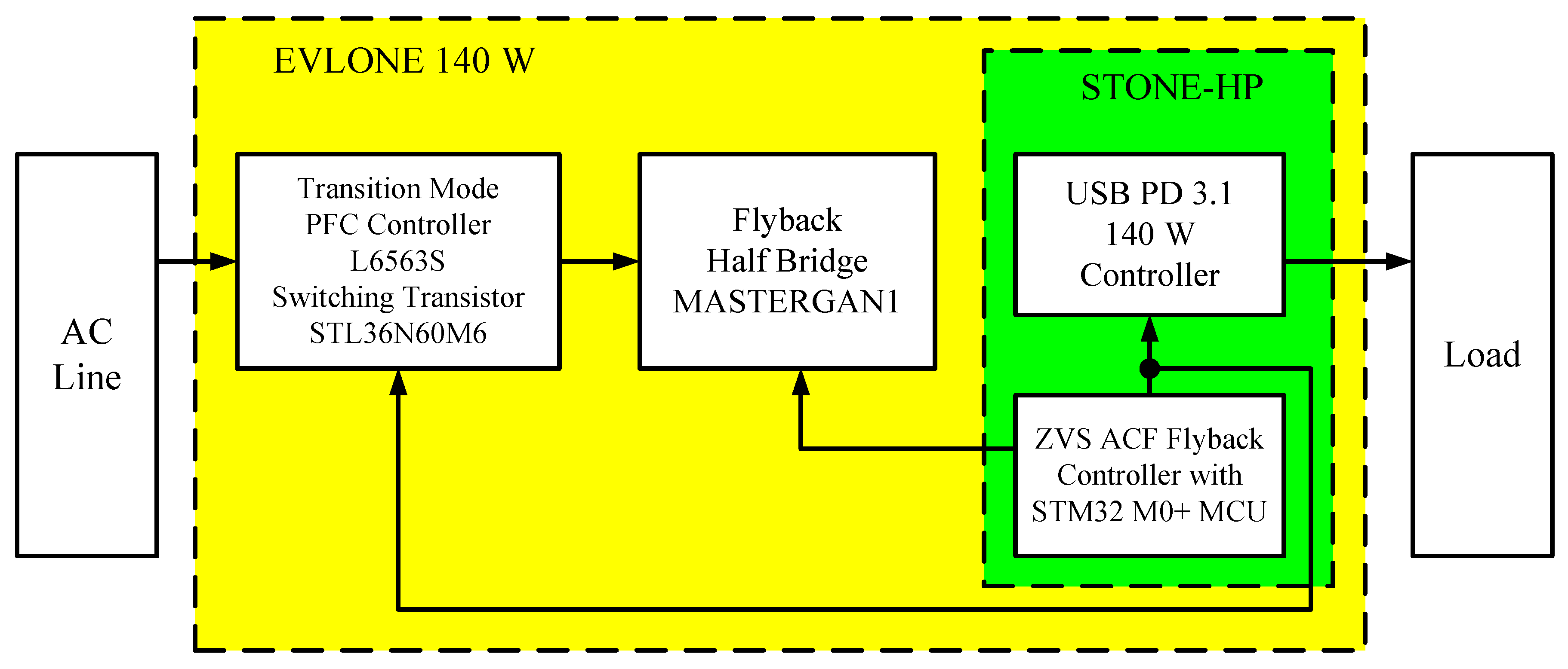
Figure 3 shows a block diagram of the set-up for measuring the performance of the EVLONE140W dedicated mobile device charging system.
The measurement system contains three interconnected functional blocks: Power supply block, Measurement block and Load block. The Power supply block contains the ATS-REG1.2 autotransformer, which allows an Alternating Current (AC) supply voltage to be obtained with an RMS value in the range from 0 to 230 V.
The Measurement block, whose main components are the TCPA300 current probe by Tektronix (Beaverton, OR, USA), records waveforms of the supply current for further Fast Fourier (FFT) analysis of these waveforms. A Pintek (Shulin, New Taipei City, Taiwan) differential voltage probe, type DP-25, is used to record the waveforms of the supply voltage of the charging system under test. The current and voltage probes operate together with a GwInstek GDS2104 oscilloscope (New Taipei City, Taiwan), whose software allows a Fast Fourier Transformation (FFT) analysis of the recorded waveforms. The RMS value of input voltage VinRMS and current IinRMS are measured by a voltmeter and ammeter, similarly to the output current Iout and output voltage Vout of the tested charging system. All the considered voltmeters and ammeters are of the type Rigol DM3058E (Suzhou, China). The values of VinRMS and IinRMD are analyzed using a Tektronix PA1000 power analyzer. This analyzer allows the coefficients of total harmonic distortion of the THDI current and THDV voltage to be measured and the power factor (PF) of the charging system under test to be measured. The Device Under Test (DUT) block contains the charging circuit under test operating in the USB PD 3.1 mode.
According to the data given by the manufacturers of the used instruments, the uncertainty of the measurements of the output voltage is described as the sum of 0.015% of the measured voltage and 0.03% of the measurement range. For the output current, the uncertainty is smaller as it is the sum of 0.25% of the measured value and 0.01% of the measurement range. In turn, the uncertainty of measurement of the RMS values of input voltage and current is smaller than the sum of 0.1% of the measured value and 0.1% of the measurement range. The uncertainty of the measurement of power is equal to the sum of 0.075% of the measured value and 0.075% of the range value. The value of uncertainty of PF depends on the phase shift between the input voltage and the input current, and it is not smaller than 0.002.
The measurement set-up analyzed also includes a Load block that allows the system under test to be loaded with a resistor from 1 Ω to 10 kΩ, as well as charging the batteries of selected mobile devices. A switch S was used to switch the type of load. In the experimental tests, the performance of the test charging system was recorded for selected State of Charge (SoC) levels from 10 to 90%.
During the experiments, two mobile devices with different battery capacities were selected. The Galaxy A23 5G smartphone (SM-A236B) manufactured by Samsung (Suwon, Republic of Korea), which contains a Li-Po battery with a capacity of 5 Ah and a voltage rating of 3.7 V, was selected as the first device for the experimental study. The other mobile device was the ThinkBook 14 G2 ITL Notebook manufactured by Lenovo (Beijing, China), which contains a Li-Po battery with a capacity of 3.8 Ah and a voltage rating of 11.55 V. The two mobile devices also differ in the maximum power with which they can be charged; for the smartphone, it is 25 W, while for the notebook, it can be as high as 65 W.
Figure 4 shows a view of the measurement set-up.
The total distortion of the current drawn from the power grid can be characterized by the total harmonic distortion coefficient,
THDI, of the supply current, which is described by the following formula [
8,
39]:
where
Ik is the
k-th harmonic of the supply current. One of the important parameters describing the performance of the selected power electronic system is energy efficiency
η, which can be calculated using the following formula [
7,
39]:
where
Pout is the output power of the power supply system under test, and
Pin is the power drawn from the power grid, the value of which was measured with a PA1000 power analyzer.
The adverse effect of time-domain disturbances in the current drawn from the power grid is usually described by the power factor (
PF) using a suitable formula implemented in a PA1000 power analyzer [
7].
where
Vin(t) and
Iin(t) denote the instantaneous values of the waveforms of voltage and current drawn from the power grid, while
VinRMS and
IinRMS denote the RMS values of voltage and current drawn from the power grid, respectively. The paper [
8] presents a method for determining the power factor using the
THDI current harmonic distortion coefficient, which was used in further experimental studies [
8].
where
THDI is the total harmonic distortion coefficient of the time course of the current drawn from the power grid and determined from the spectrum measured with a GwInstek GDS2104 oscilloscope and Formula (1).
The uncertainty of the measurement of energy efficiency is equal to the product of this efficiency and the sum of a relative error of measurement of output power and input power. In turn, the uncertainty of the measurement of
THDI factor can be estimated using the total differential method [
40]. It can be described using the following formula:
where
ΔIk denotes the uncertainty of measurement of RMS values of harmonics
Ik. The analogue formula can be used for calculating the uncertainty of
THDV.
4. Results of Measurements
Using the measurement set-up shown in
Figure 3, the characteristics of the dedicated mobile device charging system were measured. The measurement results were recorded using a PA1000 power analyzer and Rigol DM3058E multimeters, while the results used for further calculations were recorded using a GDS2104 oscilloscope. The oscilloscope software 1.19 version allowed for a Fast Fourier Transform (FFT) analysis of the recorded periodic current and voltage waveforms of the power supply, taking into account 30 consecutive harmonics. The total harmonic distortion coefficient calculations were performed by substituting the RMS values of the individual harmonics in Formula (1).
Figure 5,
Figure 6 and
Figure 7 illustrate the influence of the SoC level values of the batteries of selected mobile devices on the performance of the EVLONE140W system loaded with the two selected mobile devices, which are hereafter named Smartphone and Notebook. Detailed descriptions of the batteries used in selected mobile devices are presented in
Section 3 of the article. The values of the individual operating parameters were measured for the RMS value of the power grid voltage V
inRMS = 230 V. The black line indicates the Smartphone load, while the red line indicates the Notebook load.
Figure 5 shows the influence of the SoC level of the batteries of selected mobile devices on the RMS value of the input current I
inRMS and the value of the output current I
out.
It can be seen that the RMS value of the input current IinRMS drawn from the power grid adopts an approximately constant value regardless of the change in the SoC level of the mobile device battery, and takes on a value of approximately 0.25 A for Notebook and 0.12 A for Smartphone, respectively. The value of output current Iout for both the mobile devices under test increases as the battery’s SoC level increases, and then, after exceeding SoC = 50% (Smartphone) and SoC = 70% (Notebook), the value of output current Iout decreases to Iout = 1.27 A (Notebook) and Iout = 0.65 A (Smartphone), respectively. The observed dependence of output current Iout for both the mobile devices is qualitatively similar, but quantitatively different due to the lower permissible power that the Smartphone battery can accept, which is only 25 W in the fast charging mode.
Figure 6 shows the influence of the SoC level of the batteries of selected mobile devices on the values of THD
I and THD
V coefficients. The values of both the coefficients were determined using Formula (1), where the individual harmonics were determined using Fast Fourier Transformation (FFT) and a GDS2104 oscilloscope.
It can be observed that the highest THDI values were obtained for the current drawn from the power grid (THDI = 95.7%) when the charging system was loaded with Smartphone and its SoC level was equal to 70%. It can also be observed that the THDI value for the tested system loaded with Notebook was a slowly decreasing function of the SoC level of the battery. The changes in the value of THDI were very small. They did not exceed 1% for Smartphone and 3% for Notebook. Slightly smaller THD values were obtained for the power grid voltage. These changed in the range from 88% to 91.5%. The high values of THDI and THDV prove that the tested charging system had an adverse effect on the power grid. This system probably did not include any power factor correction circuit.
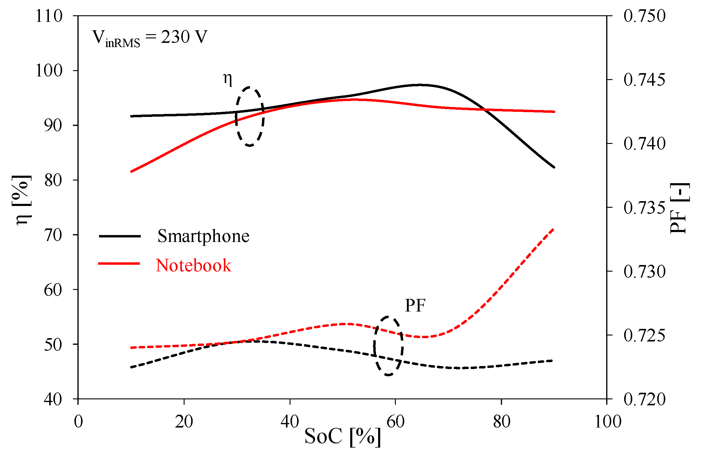
Figure 7 shows the dependence of energy efficiency η and the PF on the SoC level of the batteries of selected mobile devices. The energy efficiency value was determined using Formula (2), while the PF was determined using Formula (4).
It can be seen that the highest energy efficiency value was obtained for the dedicated charging system loaded with Smartphone for an SoC level equal to 70% and was as high as 99.6%. In contrast, the lowest energy efficiency value was obtained for the tested system loaded with Notebook for an SoC level equal to 10% and was only 81.5%. It can also be seen that the value of the PF for the tested system loaded with Notebook was an increasing function for the whole range of variations in the SoC level battery; its highest value was equal to 0.73 for an SoC level equal to 90%, and the value of energy efficiency at the same level of SoC was the highest at η = 92.5%.
The characteristics shown in
Figure 5,
Figure 6 and
Figure 7 prove that the battery charge state practically does not affect the input current value, but an increase in the SoC value results in a significant decrease in the output current value. The values of the THD
I and THD
V parameters change only slightly, by a maximum of 3%, in the entire range of changes in the SoC value. It is also worth noting that the energy efficiency of the charging system under consideration increases with an increase in the SoC value and reaches a value equal to even 95%.
Figure 8,
Figure 9 and
Figure 10 show the effect of the SoC level of the batteries of selected mobile devices on the measured waveforms of input current I
in and the spectrum of this current for the charging system loaded with two selected mobile devices. The waveforms of input current I
in were measured for the RMS value of the power grid voltage V
inRMS = 230 V and frequency f = 50 Hz. Two values of the SoC level equal to 10 and 90%, respectively, were selected for the experimental tests. The output voltage V
out of the charging system depended on the mobile device currently being charged and took on values V
out = 9 V (Smartphone) and V
out = 20 V (Notebook). The dependence of the measured input current spectrum I
in on the SoC level battery was presented as the ratio of the individual harmonics to the value of the fundamental harmonic amplitude of the supply current waveform. In the experimental study of input current spectrum I
in, both odd and even harmonics were presented.
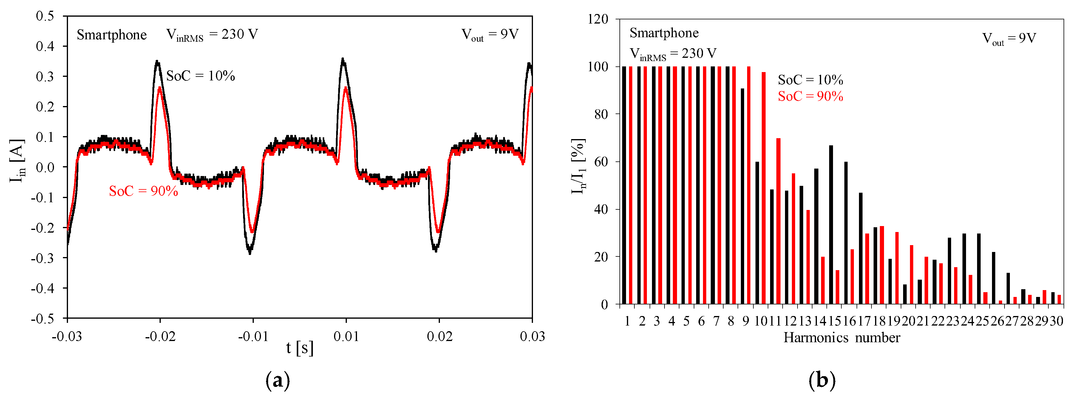
Figure 8 shows the waveforms of input current I
in (a) and the input current spectrum (b) as a function of the SoC level of the built-in battery in the smartphone. The output voltage V
out during the battery charging process was equal to approximately 9 V.
Analyzing
Figure 8a, it can be observed that the time waveforms of I
in current are highly distorted and do not resemble sinusoidal waveforms regardless of the charge level of the selected mobile device. It should be noted that a higher peak-to-peak value of input current I
in drawn from the power grid was obtained for SoC equal to 10% and was I
inpp = 0.64 A, and a lower value of 0.48 A was obtained for SoC equal to 90%. The mentioned peak-to-peak value was equal to the difference between the maximum and minimum values of the considered waveform.
Analyzing
Figure 8b, it should be noted that regardless of the SoC level of the Smartphone battery, the spectrum of the input current waveform had large normalized harmonic values. For SoC equal to 90%, it can be noted that as many as nine harmonics of the fundamental frequency had the maximum amplitude. It should also be noted that the large amplitude values of the individual harmonics corresponded to very strongly distorted waveforms of input current I
in regardless of the SoC of the mobile device battery.
Figure 9 shows the waveforms of input current I
in (a) and the input current spectrum (b) as a function of the battery SoC used in Notebook. The output voltage V
out of the dedicated charging circuit during the battery charging process was approximately 20 V.
Analyzing
Figure 9a, it should be noted that a lower peak-to-peak value of input current I
inpp = 0.62 A was obtained for SoC equal to 90%, while for SoC equal to 10%, the peak-to-peak current value was higher at 0.83 A, which is related to the start of the charging process of the battery used. As the SoC of the battery increased, the charging current decreased. It can also be seen that the waveform of the input current I
in was still far from a sinusoidal shape.
Analyzing
Figure 9b, it should be noted that, regardless of the SoC level of the Notebook battery, the spectrum of the input current contained large normalized values of consecutive harmonics. For SoC = 10%, we can observe that as many as nine harmonics of the fundamental frequency had a value significantly close to the maximum amplitude. It should also be noted that the large values of the amplitudes of the individual harmonics correspond to highly distorted waveforms of the input current drawn from the power grid regardless of the SoC level of the Notebook battery.
Figure 10 compares the waveforms of input current I
in (
Figure 10a) and the input current spectrum (
Figure 10b) for two arbitrary selected loads in the form of mobile device batteries Smartphone and Notebook, respectively. The output voltage V
out of the charging system during the charging process of the Smartphone battery was equal to approximately 9 V, while that of Notebook was equal to approximately 20 V. The SoC level of both the batteries during the analysis of the waveforms of input current I
in and the spectrum of the current under test was equal to 50%.
Analyzing
Figure 10a, it can be seen that the recorded input current waveforms are heavily distorted and do not resemble a sinusoidal waveform in their shape. It should be noted that the highest peak-to-peak value of the input current (I
inpp = 0.82 A) was obtained for the charging system loaded with the Notebook battery, while when using the Smartphone battery as the load, the current value was 45% lower and amounted to I
inpp = 0.46 A. The different peak-to-peak values of input current I
in are the result of the different power supplied to the batteries of the selected mobile devices during the tests.
In
Figure 10b, it should be noted that the spectrum of the input current waveform contains significant normalized harmonic values. In the case of loading the tested system with the Smartphone battery, we can observe that as many as nine harmonics of the fundamental frequency contained a value significantly close to the maximum amplitude. It should also be noted that the large values of the amplitudes of the individual harmonics correspond to highly distorted waveforms of input current I
in drawn from the power grid regardless of the type of load. It can also be noted that the 30 harmonic bars of the fundamental frequency are presented in the experimental study, and the value of the amplitude of 30 harmonic bars is quite high at about 15% of the amplitude of the first harmonic bar.
Comparing the results presented in
Figure 8,
Figure 9 and
Figure 10, it can be seen that for the load containing a smaller capacity battery (Smartphone), much larger distortions were visible than for Notebook. It can also be seen that the input current distortions were smaller at higher SoC values.
It is also worth noting that the value of the battery charging current also depends on the value of its internal resistance. This resistance limits the maximum value of the charging current, and its increase results in an extension of the charging time [
27]. This limitation translates into a limitation of the input current amplitude of the charging system and a reduction in the distortion of this current.
Figure 11,
Figure 12 and
Figure 13 show the influence of the load resistance R
o on the operating parameters of the charging system. The values of individual operating parameters were measured for the RMS value of the power grid voltage V
inRMS = 230 V and for three selected values of output voltages V
out equal to 5, 9, and 20 V, respectively. Changing the output voltage V
out would not be possible without the use of an external USB PD 3.1 port triggering system. In [
41], the full technical and operational documentation of the COM-ZY12PDN Trigger the USB PD 3.0 system was presented, which allows the dedicated charging system to operate without a connected mobile device and allows output voltage V
out to be changed within a set range not exceeding 20 V for the tested system. This system acted as a system negotiating the level of the output voltage normally used in mobile devices.
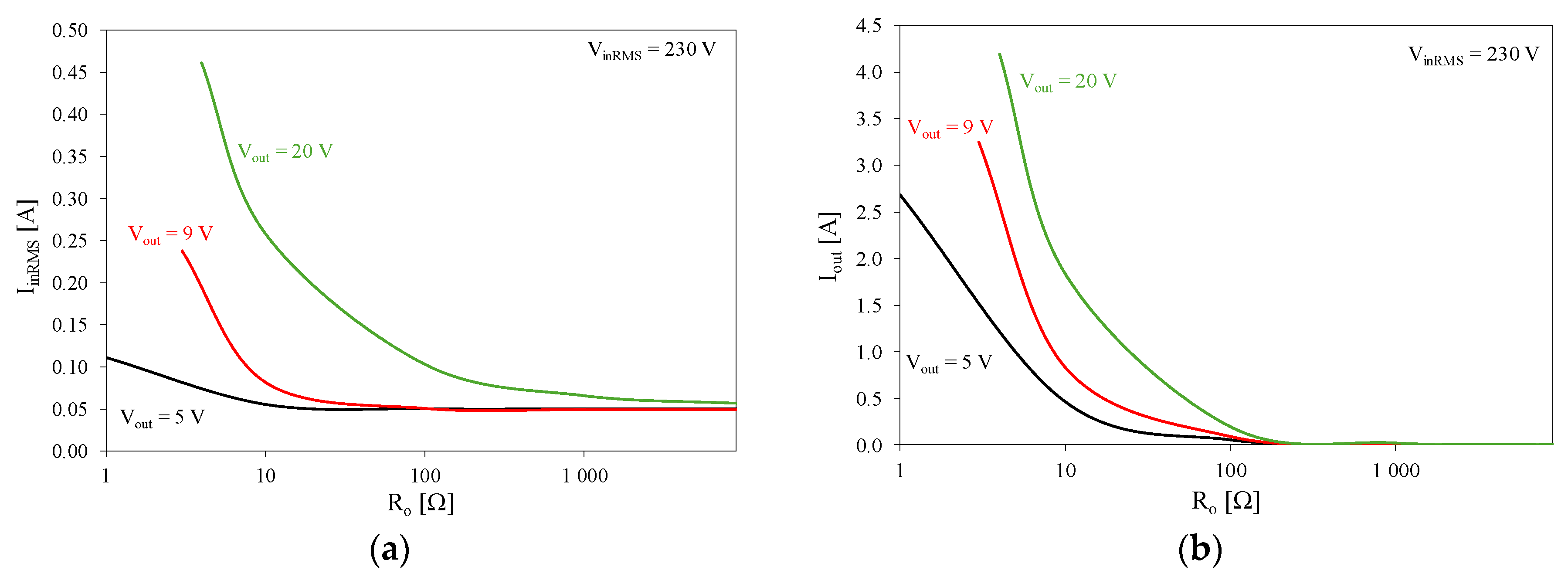
Figure 11 shows the influence of load resistance R
o on the RMS value of the input current I
inRMS (
Figure 11a) and output current I
out (
Figure 11b).
Analyzing the dependences shown in
Figure 11, it can be seen that they are a decreasing function of load resistance R
o regardless of output voltage V
out.
Figure 11a shows that the highest RMS value of input current I
inRMS equal to 0.46 A was obtained for the charging system operating with output voltage V
out = 20 V and load R
o = 4 Ω, while a much smaller value of I
inRMS = 0.11 A was obtained for output voltage V
out = 5 V and load resistance R
o = 1 Ω. The lowest effective value of input current I
inRMS, about 50 mA, was obtained for resistance R
o = 10 kΩ, for all three values of output voltages V
out.
In
Figure 11b, one can see the identical shape of I
out(R
o) dependence as in
Figure 11a, while the values of output current I
out are much higher than in the case of the dependence from
Figure 11a. For load resistance R
o = 4 Ω and output voltage V
out = 20 V, output current was equal to 4.2 A.
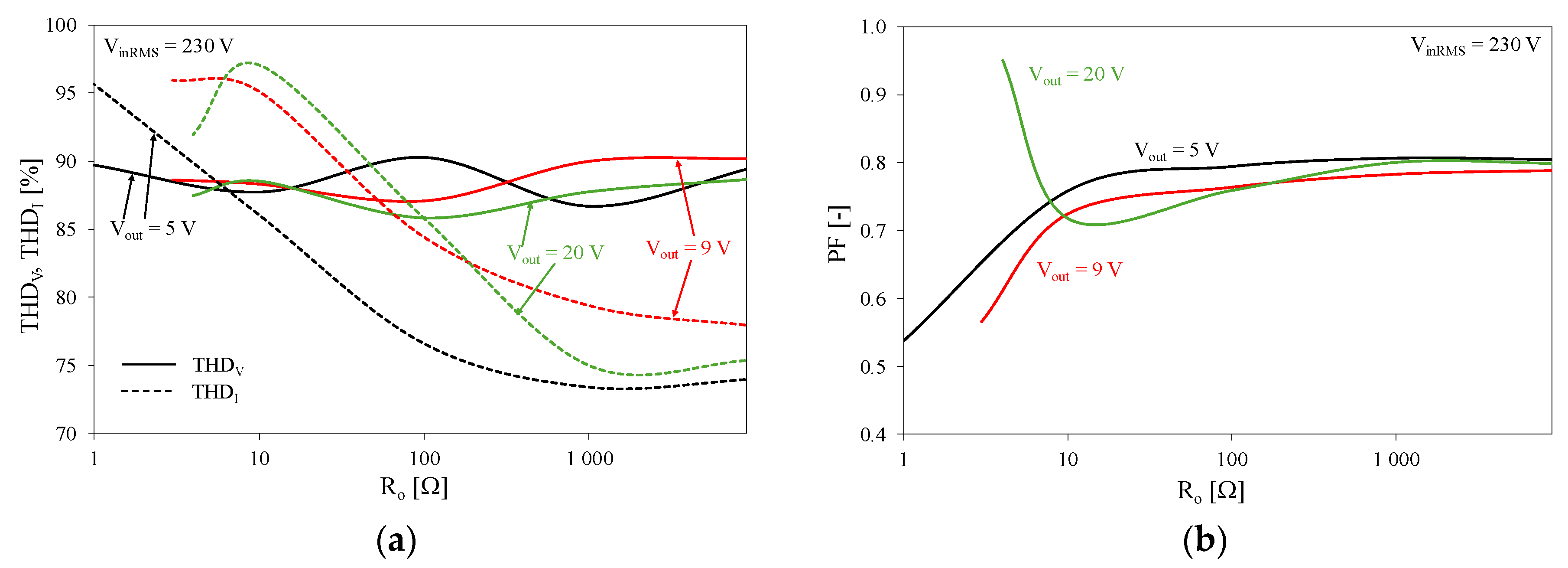
Figure 12 illustrates the influence of load resistance R
o on the total harmonic distortion value THD of the voltage and current drawn from the power grid (a) and the power factor PF (b) for three different values of output voltage V
out. The value of THD was calculated using Formula (1), while the PF value was calculated using Formula (4).
In
Figure 12a, it can be seen that, in the whole range of changes in load resistance R
o, the dependence of both the THD coefficients on R
o is a decreasing function. It can be seen that the power network voltage THD
V in the whole range of changes in R
o changes only by 5%, while the value of the total harmonic content of the current THD
I changes by as much as 18.5%. The highest value of the THD
I was obtained for the considered system operating with output voltage V
out = 20 V (THD
I = 92% @ R
o = 4 Ω), while the lowest value of the THD
I was obtained for the tested system operating with V
out = 5 V (THD
I = 73.4% @ R
o = 1 kΩ).
In
Figure 12b, it can be seen that the biggest changes in the power factor value were observed for load resistance R
o changing in the range from 1 to 10 Ω. The highest value of the power factor PF = 0.95 was obtained for the charging system operating with load resistance R
o = 4 Ω and output voltage V
out = 20 V. For the load resistance R
o in the range from 1 kΩ to 10 kΩ, the power factor stabilizes at a value of about 0.8.
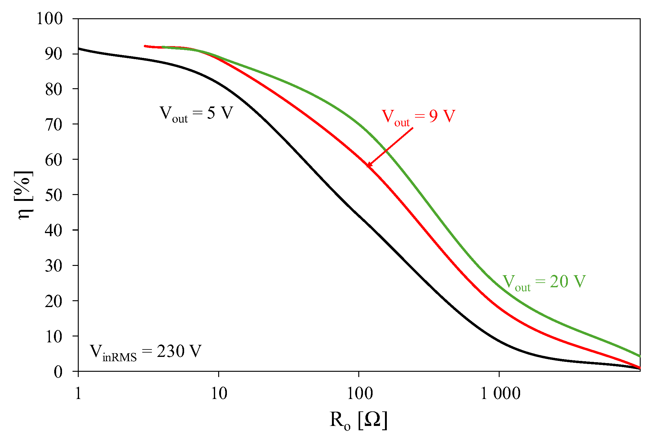
Figure 13 illustrates the influence of load resistance R
o on energy efficiency η of the tested EVLONE140W system for three different values of output voltage V
out. The value of η was calculated using Formula (2).
In
Figure 13, it can be seen that the dependence of energy efficiency η of the tested system is a decreasing function of load resistance in the whole range of R
o changes regardless of output voltage V
out. With an increase in the output voltage, the energy efficiency increases. Its highest value η = 91.9% was obtained for V
out = 20 V and R
o = 4 Ω.
In
Figure 11,
Figure 12 and
Figure 13, it can be seen that, at higher values of the output voltage, higher values of the energy efficiency and the input and output current were obtained. The energy efficiency was higher in the range of low values of load resistance. At high values of load resistance, PF values practically did not depend on the value of V
out voltage.
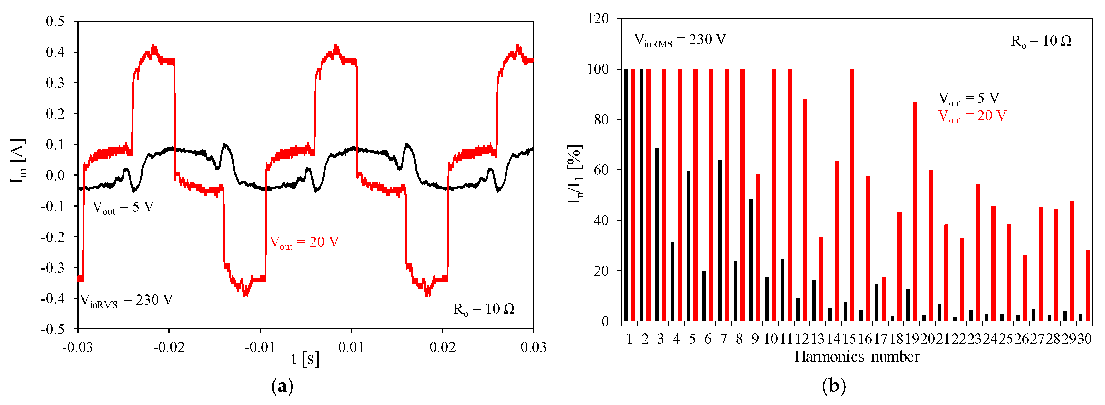
Figure 14 and
Figure 15 present the influence of load resistance (
Figure 14) and the output voltage (
Figure 15) on the waveforms of input current I
in drawn from the power grid by the tested system. Experimental studies were carried out for the power grid voltage V
inRMS = 230 V.
Figure 14 presents the studies carried out for two different values of load resistance R
o equal to 10 Ω and 1 kΩ, respectively, and for output voltage V
out = 20 V.
In
Figure 14a, it should be noted that the highest peak-to-peak value of input current I
inpp = 0.82 A was obtained for load resistance R
o = 10 Ω, and the lowest value I
inpp = 0.16 A for load resistance R
o = 1 kΩ. In turn, in
Figure 14b, it can be observed that the highest normalized values of the harmonics in the spectrum of current I
in were obtained for R
o = 10 Ω. During the tests, up to 15 harmonics with the maximum normalized value were recorded, which confirms the high level of distortion of current I
in. In turn, for the considered values of load resistance, only the first and second harmonics with the maximum normalized value could be observed, and higher harmonics had an increasingly smaller amplitude.
Figure 15 presents the test results carried out for two values of output voltage V
out equal to 5 and 20 V, respectively, and for load resistance R
o = 10 Ω. Analyzing
Figure 15a, it should be noted that the highest peak-to-peak value of the input current I
inpp = 0.82 A was obtained for output voltage V
out = 20 V, and the lowest value I
inpp = 0.15 A for V
out = 5 V.
In
Figure 15b, it can be seen that the largest normalized values of harmonics of the spectrum of current drawn from the power network were obtained for output voltage V
out = 20 V. In turn, for output voltage V
out = 5 V, only the first and second harmonics with the maximum normalized value could be observed. The subsequent harmonics had increasingly smaller amplitudes.
The results presented in
Figure 14 and
Figure 15 show that the input current of the charging system is much less distorted when operating at low output voltage and high load resistance. Unfortunately, these are not typical operating conditions for such a system and can be observed when the load is a low-voltage battery in a state close to full charge.
The investigations results presented in this section refer only to room temperature. As demonstrated in the paper [
27], temperature significantly affects the characteristics of charging and discharging of batteries and their electric capacity. Similarly, in the paper [
42], it was found that the properties of switch-mode power supply systems can significantly change when the junction temperature of their components changes. However, thanks to the use of specialized control systems and compensatory properties of the feedback loop, it is possible to ensure the desired parameters of the battery charging current.


