Article

Design and Analysis of Micro Signal Detection Circuit for Magnetic Field Detection Utilizing Coil Sensors

1
College of Engineering Science and Technology, Shanghai Ocean University, Shanghai 201306, China
2
Shanghai Engineering Research Center of Marine Renewable Energy, Shanghai 201306, China
*
Author to whom correspondence should be addressed.
Appl. Sci. 2024, 14(9), 3618; https://doi.org/10.3390/app14093618
Submission received: 24 March 2024 / Revised: 12 April 2024 / Accepted: 12 April 2024 / Published: 25 April 2024
(This article belongs to the Special Issue Electromagnetic Detection Instruments and Signal Processing)

Abstract

:
Eddy current inspection has been extensively employed in non-destructive testing of various conductive materials. The coil probe, as a mainstream sensor in the eddy current detection system, inevitably encounters interference from external signals while transmitting its own signal. Therefore, developing techniques to extract valuable signals from noisy ones is crucial for ensuring accurate detection. Carbon fiber composites not only possess significantly lower electrical conductivity compared to conventional metallic materials but also exhibit notable anisotropy. To address this issue, we designed an ‘8’ coil probe set where the excitation coil does not electromagnetically interfere with the detection coil. However, practical applications that require portability and miniaturization pose challenges when utilizing this coil probe set to identify carbon content or defects due to the typically weak output signal. To address this issue, this paper proposes a design that combines the ‘8’ structure of the planar coil probe with the principle of phase-locked amplification to create a dual-phase sensitive phase-locked amplification detection circuit. These specific design ideas were tested using a weak signal, which passed through the preamplifier, secondary amplifier, and band-pass filter comprising the target channel for signal amplification and noise filtering. The effective signal amplitude is proportional to the inverse phase difference between the direct current (DC) signal and inversely proportional to the amplitude of the signal. Finally, the DC signal was passed through an analog-to-digital converter (ADC). The analog-to-digital converter (A/D) is used to collect and calculate the DC signal, enabling the detection of weak electrical signals. Simulation experiments demonstrated that the signal detection circuit has an amplitude error below 0.2% and a phase error below 0.5%. The phase-locked amplification circuit designed in this paper can effectively extract the tiny impedance change signals of the planar coil sensor probe with high sensitivity and good robustness.

1. Introduction

Carbon Fiber-Reinforced Plastics (CFRP) are composite materials composed of carbon fibers and a resin matrix. Compared to metal materials, carbon fiber composites have many advantages. They have low density and high strength [1]. In comparison to conventional steel, their service life is extended by 2–3 times, and their tensile strength can reach up to 3500 MPa, which is five times that of steel [2]. Carbon fiber has several advantages, including a small coefficient of thermal expansion, good thermal conductivity, high and low temperature resistance, and good resistance to sudden changes in temperature [3]. Due to these excellent characteristics, it is widely used in high-precision technology fields such as aerospace, ocean-going ships, rail transportation, and new energy vehicles [4].
Although CFRP have excellent properties, defects may occur during production or due to external environmental factors. The complexity of CFRP processing and factors such as low molecular impurities in the prepreg, solvents, and moisture volatilization can contribute to the formation of these defects [5]. These defects, such as voids, cracks, and delaminations, can significantly reduce the serviceability of the component and shorten its life. The development of nondestructive testing technology for CFRP materials is significant. Some scholars have improved the sensitivity of the inspection coil by designing specific coil structures. Wang et al. analyzed the impedance of rectangular planar coils and bending-type coils through finite element numerical analysis and compared the results with experimental data to reveal the influence of different coil parameters on impedance [6]. Abderraouf Bouloudenine proposed a circular array sensor including 16 coils [7]; this method effectively reduces noise due to mechanical rotation and is able to efficiently capture the texture characteristics of the fibers. Miguel A. Machado experimentally used a pair of 45° parallelogram coils on CFRP with low conductivity in tests; minimal side cuts and fiber breaks were detected, and the experiments showed a good signal-to-noise ratio [8]. For the detection of curved pipes with natural concave defects, Daura, L. U., proposed a transmit–receive Flexible Printed Coil (FPC) array using the Wireless Power Transfer (WPT) method for a material surface using the WPT principle. The single excitation coil and multiple receiving coils of the material surface were experimentally investigated for mapping and reconstruction of defective depressions for quantitative nondestructive inspection through feature selection and feature fusion by deep learning [9]. Lefebvre et al. fabricated a rectangular planar inductive coil with a wire diameter as small as 10 μm. They then simulated and analyzed the magnetic field around the coil using FEM software (ANSYS® version 12.1). The coil was successfully used to capture and manipulate magnetic particles [10]. When a magnetic sensor measures a magnetic field, the signal strength at the receiving end may vary due to changes in the distance between the probe and the test sample, leading to uncertain results. To address this issue, Dehui Wu and colleagues developed a specialized probe that features an ‘8’-shaped transmitting coil and a circular receiving coil. This probe is highly sensitive in detecting defects and is not affected by changes in lift-off distance [11]. This signal is often submerged in a larger background signal composed of the ambient magnetic field and circuit noise. The detection and extraction of a weak magnetic field signal is a crucial part of nondestructive CFRP testing technology. In addition to the probe structure and lift-off effect mentioned above, one way to solve this problem is through the use of a phase-locked loop. Zhaoyin Li et al. proposed a scheme for detecting weak Radio Frequency (RF) signals based on a single-mode Opto-Electronic Oscillator (OEO). To avoid the injection locking phenomenon, they used a Phase-Locked Loop (PLL) structure, which ensured that the OEO operated under quasi-locked conditions. The RF signal detected in their work provided a maximum gain of 59.49 dB and a detection sensitivity of −120 dBm [12]. Li et al. (2023) generated a 1550/1560 nm two-color electro-optical frequency comb by modulating two continuous-wave lasers using a common electro-optical modulator and phase-locking their beat frequencies. They effectively suppressed the phase noise of the frequency comb modes accumulated from the RF synthesizer [13]. Geng Xinlin et al. introduced a 25.8 GHz integer-N Charge Pump Phase-Locked Loop (CPPLL) that demonstrates strong locking performance. The proposed Time-Amplified Phase-Frequency Detector (TAPFD) greatly suppresses in-band noise through phase error amplification gain [14].
This paper investigates the structural optimization, signal detection, and extraction difficulties of coil sensor probes in CFRP eddy current non-destructive testing (NDT) systems. The ‘8’ type structure probe was improved by adopting an ‘8’ type structure planar coil probe sensor, which is more sensitive to electric signals for signal acquisition. The study delves into the composition of lock-in amplifiers based on the principle of phase-locked amplification. A dual-phase-sensitive lock-in amplifier circuit was developed to overcome the difficulty of single lock-in amplifiers that require accurate phase adjustment. The circuit was verified through simulation experiments.

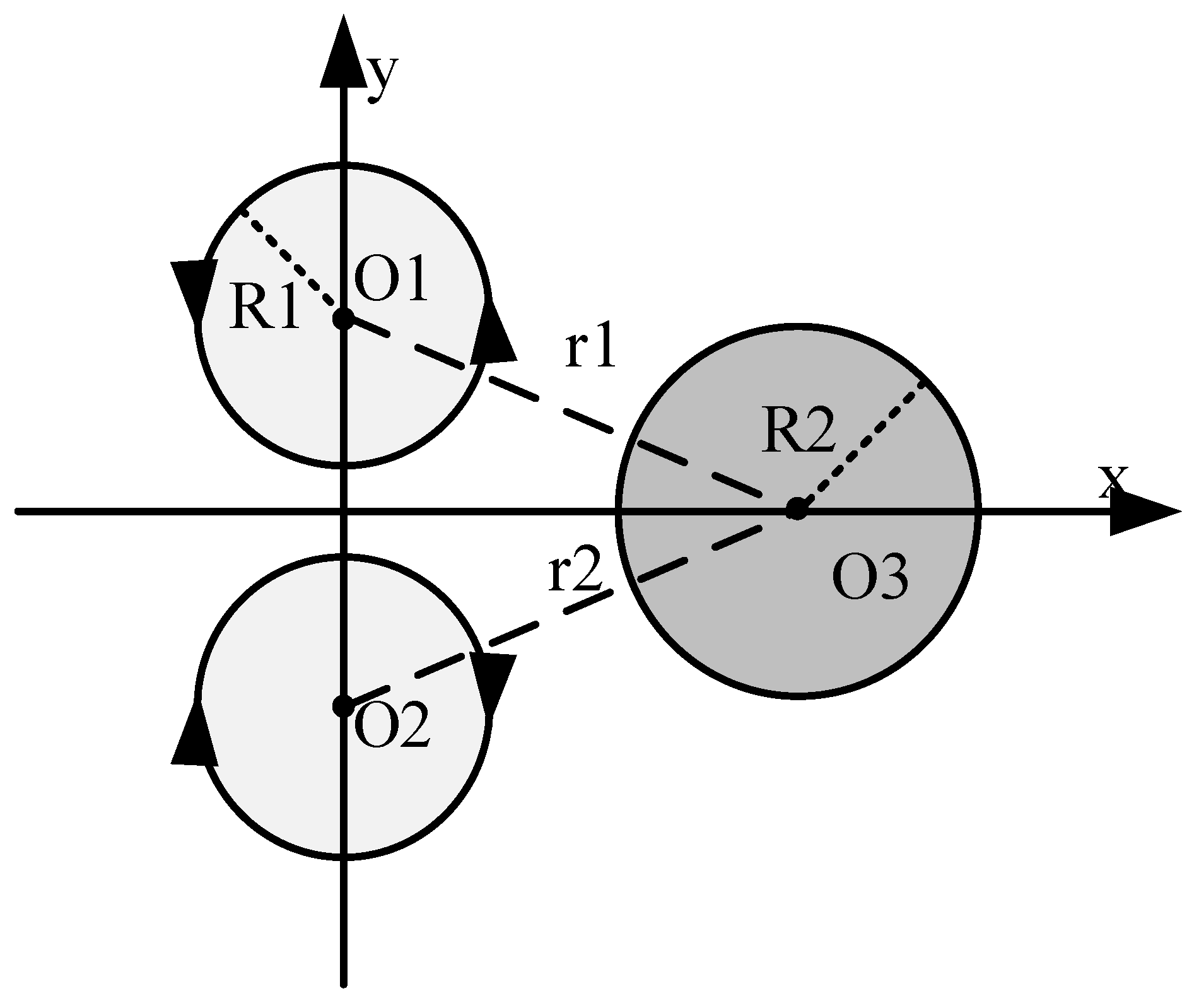
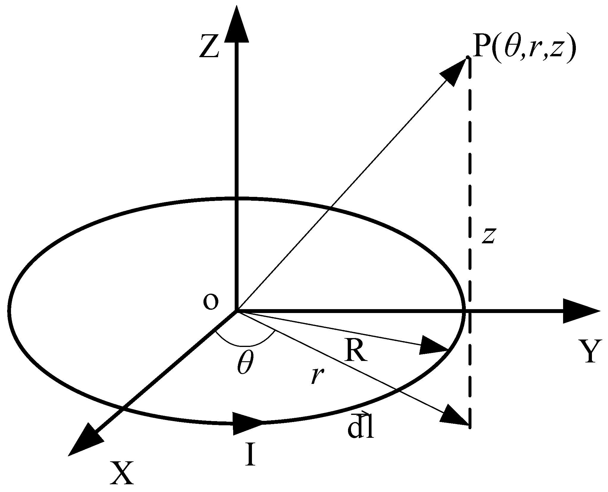
2. Eddy Current Detection

Eddy Current Testing (ECT) is an NDT method that uses electromagnetic induction. An excitation coil with alternating current is placed near the surface of the conductive material to generate an alternating magnetic field. This field induces a ring current, known as the eddy current, within the conductor being tested. The eddy current generates another magnetic field that impacts the original magnetic field, causing a change in the magnetic flux within the detection coil. This change can be measured via the alteration in impedance in the detection coil. The coil’s equivalent impedance can typically be expressed as a function of Equation (1) [15].
Z = F σ , μ , f , x , r
where σ, μ are the electrical and magnetic conductivity of the conductor under test, respectively; f is the frequency of the excitation signal; x is the coil lifting distance; and r is the radius of a coil. It can be seen that changes in coil impedance reflect changes in the physical properties of the conductor material. For example, when detecting defects on the surface of a conductive material, due to the presence of defects, both the electrical and the magnetic permeability of the material change, which in turn leads to changes in the impedance parameters of the coil. Due to the conductive nature of carbon fiber composites, electromagnetic eddy current detection enables the detection and analysis of geometric and physical properties of composites such as fiber orientation, layup order, and conductivity [16,17].
In eddy current detection, the design of the coil probe is crucial to ensure the effectiveness of the eddy current detection method. This section provides a theoretical analysis of the planar coil probe used. Figure 1 illustrates a planar projection of the “8” coil structure, where coils 1 and 2 serve as excitation coils, and coil 3 functions as the receiving coil. O1 and O2 denote the centers of the two excitation coils, while O3 is located on the vertical bisector of O1O2. The radius of the excitation coils is represented by R1, the radius of the receiving coil by R2, and r1 and r2 denote the distances from the center of the receiving coil to those of the two excitation coils. The excitation coils share identical parameters except for the direction of their internal currents and are positioned along the vertical bisector of their center lines. Therefore, the magnetic flux generated by each excitation coil within the influence range of a receiving coil should be equal in size but opposite in direction. As a result, there should be no impact or interference with signal reception by the receiving coil.
The magnetic field distribution of a circular planar coil can be viewed as a superposition of the magnetic fields generated by concentric current rings of different diameters. Figure 2 shows the spatial magnetic field distribution for a single current ring. In the figure, the XYZ coordinate system is constructed with the center of the coil as the origin, and R represents the polar coordinates of any point P in the radius space of a single current loop as (θ,r,z). A multiturn planar helical coil can be approximated as a superposition of concentric rings with different radii. The magnetic field distribution of a multi-turn coil can be obtained. At the center of the nth-turn coil, denoted by point P, the magnetic field strength is given by Equation (2):
H N ( z ) = n = 1 N I R n 2 2 ( R n 2 + d 2 ) 3 / 2
where d is the distance from point P to the center of the coil, which can be calculated quite simply using the polar formula; Rn is the radius of the nth-turn coil.
However, due to the limitation of the structure’s size, the small inductance and large resistance of the sensor make signal acquisition and detection difficult. Therefore, in this paper, we used frequency-specific filtering of the output signal to obtain an effective signal [18], and a lock-in amplifier [19] realized by using the frequency-transformed heterodyne technique to significantly improve the Q value. Based on the above principles, this paper developed a new phase-locked amplifier circuit suitable for detecting the signals of planar coil probe sensors for low-conductivity carbon fiber-reinforced resin materials, and conducted in-depth theoretical analysis and simulation experimental research on it.

3. Principle of the Weak Signal Detection Circuit

The lock-in amplifier principle uses the frequency difference between the output signal and the noise signal to correlate the target signal, thereby achieving detection of weak signals [20]. The eddy current detection coil’s output detection signal S(t) consists of the effective signal E(t) and the noise signal n(t):
E ( t ) = V s s i n ( ω s t + ϕ s )
where Vs is the effective signal amplitude, ωs is the effective signal frequency, ϕs is the effective signal phase angle; therefore the output signal is Equation (4) and the reference signal is Equation (5):
S ( t ) = E ( t ) + n ( t )
R ( t ) = V r s i n ( ω r t + ϕ r )
where Vr is the amplitude of the reference signal, ωr is the frequency of the reference signal, ϕr is the phase angle of the reference signal, and the output signal obtained by performing a multiplication operation between S(t) and R(t) is denoted V p s d ( t ) :
V p s d ( t ) = V s V r 2 c o s [ ( ω s ω r ) t + ( ϕ s ϕ r ) ] V s V r 2 c o s [ ( ω s + ω r ) t + ( ϕ s + ϕ r ) ] + V r n ( t ) s i n ( ω r t + ϕ r )
The first two items are valid signals, the latter is a signal with noise effects, the frequency of the valid signal ωs is equal to the frequency of the excitation signal ω, and the frequency of the reference signal ωr is set to ω; thus, Equation (6) can be simplified to Equation (7):
V p s d ( t ) = V s V r 2 c o s ( ϕ s ϕ r ) V s V r 2 c o s ( 2 ω t + ϕ s + ϕ r ) + V r n ( t ) s i n ( ω t + ϕ r )
From Equation (7), it can be obtained that the signal after phase-sensitive detection is divided into three terms: the first term is the DC component, and the second and third terms are the high-frequency AC components. The output signal V o u t is obtained after low-pass filtering of V p s d ( t ) :
V o u t = V s V r 2 c o s ( ϕ s ϕ r )
From Equation (8), it can be seen that the magnitude of Vout is related to the amplitude and phase of E(t), which are proportional to the amplitude and cosine of the phase difference between the effective signal and the reference signal. To mitigate large phase differences caused by discrepancies in output signal amplitudes, we employ Equation (9) for the reference signal R′(t) and perform aforementioned processing on both the reference and output signals, resulting in Vout depicted in Equation (10):
R ( t ) = V r s i n ( ω r t + ϕ r + π 2 )
V o u t = V s V r 2 s i n ( ϕ s ϕ r )
where Vout is the in-phase component and Vout is called the quadrature component. Therefore, the amplitude Equation (11) and the phase difference Equation (12) are obtained.
V S = 2 ( V o u t 2 + V o u t 2 ) V r
Δ ϕ = ϕ s ϕ r = t a n 1 ( V o u t V o u t )
A lock-in amplifier consists of a target signal channel, a reference signal channel, and a correlator channel. From Equation (8) it can be seen that, in a single lock-in amplifier, the final output signal can be controlled by adjusting the phase of the reference signal and thus the value of the phase difference [21]. In studying the principle of lock-in amplification, it is noted that a single lock-in amplifier requires precise adjustment of the phase. In order to realize efficient processing of the weak signals from planar coil sensors, a circuit structure for the dual lock-in amplifier was adopted in this paper. As shown in Figure 3, two phase shift detectors (PSDs) were introduced, each of which used a reference signal with a phase difference of 90° to multiply with the target signal. This design greatly improves the processing efficiency of the weak signals of the planar coil sensor.

4. Hardware Design of Dual-Phase Sensitive Lock-in Amplifier Circuits

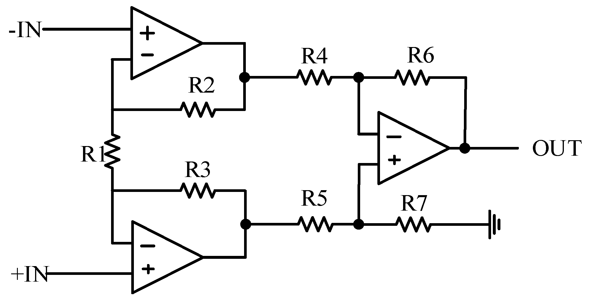
4.1. Pre-Differential Amplifier Circuit

The task of the target signal channel is to amplify the input signal to ensure that the amplitude of the target signal reaches the operating voltage required by the detection circuit, while minimizing the interference of various types of noise and DC drift, so that the signal input to the correlator channel is maintained in a low-noise and low-distortion state. In this paper, a Texas Instruments model OPA656 operational amplifier was used, which has excellent characteristics including high gain-bandwidth product, low input bias voltage, and low input voltage noise. The preamplifier circuit in the target amplifier uses differential amplification. As shown in Figure 4, at the signal input, two voltage followers with gain are introduced to achieve efficient amplification of the input voltage, and then the differential amplification circuit is used for differential operation to output the processed signal, which is designed to effectively increase the amplitude of the target signal.
When this circuit R2 = R3, R4 = R5, R6 = R7, its structure is approximated to an upper and lower symmetrical structure; then, the output signal Uo is given in Equation (13):
U O = R 6 R 4 1 + 2 R 2 R 1 U + U
where U and U+ are electrical signal inputs.

4.2. Bandpass Filter Circuit

The signal passes through the differential amplifier and enters the bandpass filter module, which filters out most of the interfering signals, reducing the load on the chip and improving the signal-to-noise ratio. As shown in Figure 5, the bandpass filter module consists of two amplifiers, which can meet the requirements of high Q to ensure excellent filtering effect, thus guaranteeing improvement in signal quality.
When C1 = C2 = C3, R2 = R3 = R, R4 = R5 in this circuit module, the transfer function T(s) is Equation (14):
T ( s ) = s 2 R C s 2 + 1 R 1 C s + ( 1 R C ) 2
The center frequency f0 and Q of the bandpass filter can be determined using the resistance and capacitance values, as shown in Equation (15). This calculation is based on the transfer function.
f 0 = 1 2 π C R 2 ; Q = R 1 R 2
In ECT detection, it is crucial to ensure that the frequency of the effective signal matches that of the excitation signal. For instance, if the excitation coil operates at a frequency of 1 MHz, then the eddy current generated on the surface of CFRP prepreg should also have a frequency of 1 MHz. Consequently, it is essential for the detector coil to detect an effective signal with an amplitude and frequency of 1 MHz as well. Therefore, maintaining an f0 identical to the excitation signal’s frequency is imperative. However, aiming for high precision by setting a very high Q value (narrowing down the cut-off bandpass) can place excessive demands on electronic components. Hence, relying solely on a bandpass filter to eliminate interference signals becomes unfeasible. Additional modules such as multipliers and low-pass filters are required to further reduce noise.

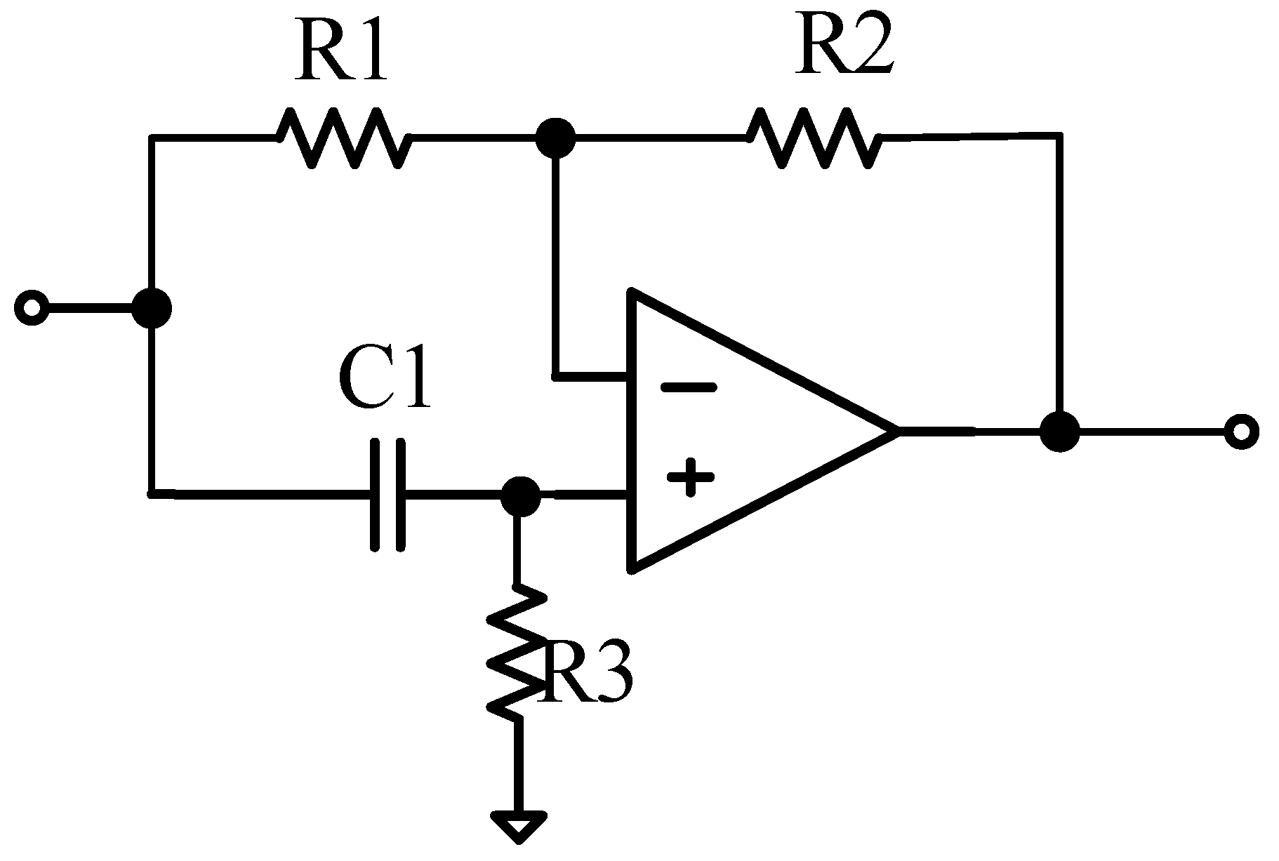
4.3. Circuit of Phase Shift

After the reference signal passes through the amplifier, it has two different paths: one goes directly to the phase-sensitive detector that participates in the multiplication operation; the other passes first through a 90° phase shifter and then to another phase-sensitive detector for multiplication. The phase shifter here is a special type of all-pass filter whose gain frequency characteristics are fixed and do not filter out noise, but whose phase frequency characteristics are changed. Therefore, it is usually used in situations where the phase of the signal needs to be changed without changing the amplitude of the signal. In this paper, we used the all-pass filter technique to design this 90° phase shifter, the structure of which is shown in Figure 6.
When R1 = R2, R3 = R, C1 = C in this circuit module, the transfer function T(s) is Equation (16)
T s = 1 + s R C 1 + s R C
From (16) can be introduced gain A = 1, and the phase change relationship ψ is Equation (17).
ψ = arctan ( 2 ω R C ( ω R C ) 2 1 )
Bringing ω = 1 R C into Equation (17) gives Equation (18).
ψ = arctan ( 2 ω R C ( ω R C ) 2 1 ) a r c t a n = 1 2 π
Based on Equations (15) and (17), the phase shifter module can shift the phase angle of signals by 90° without altering the amplitude of the reference signals. This allows for the acquisition of a set of reference sub-signals that are orthogonal to each other. These two sets of signals are fed into two different phase-sensitive detectors together with the target signal.

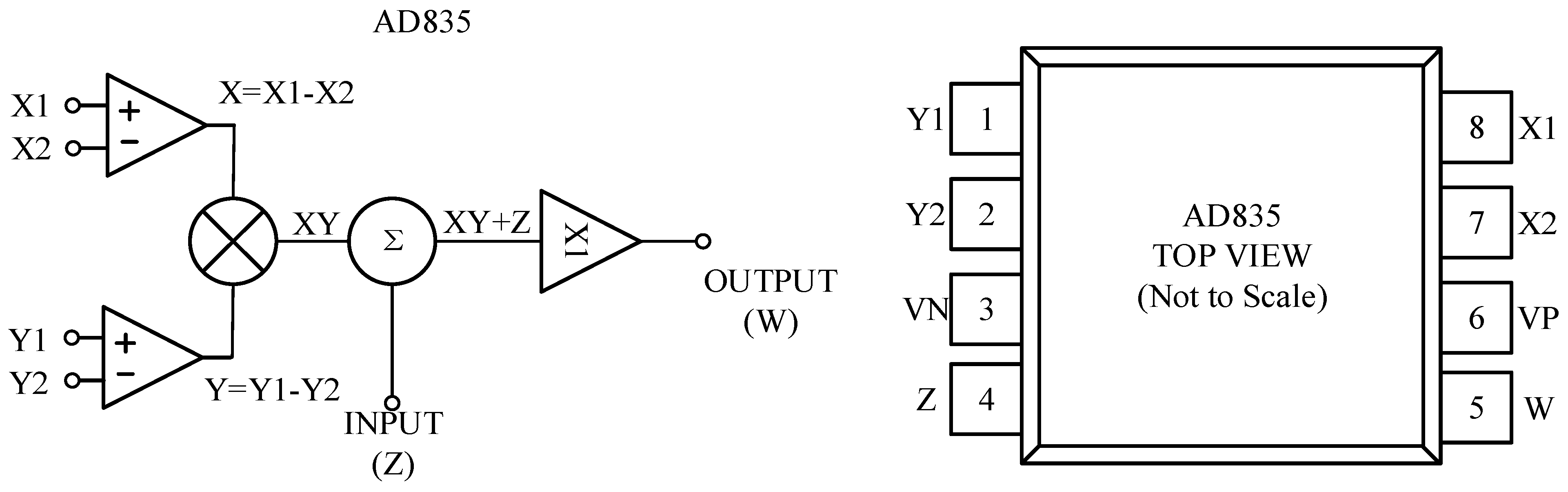
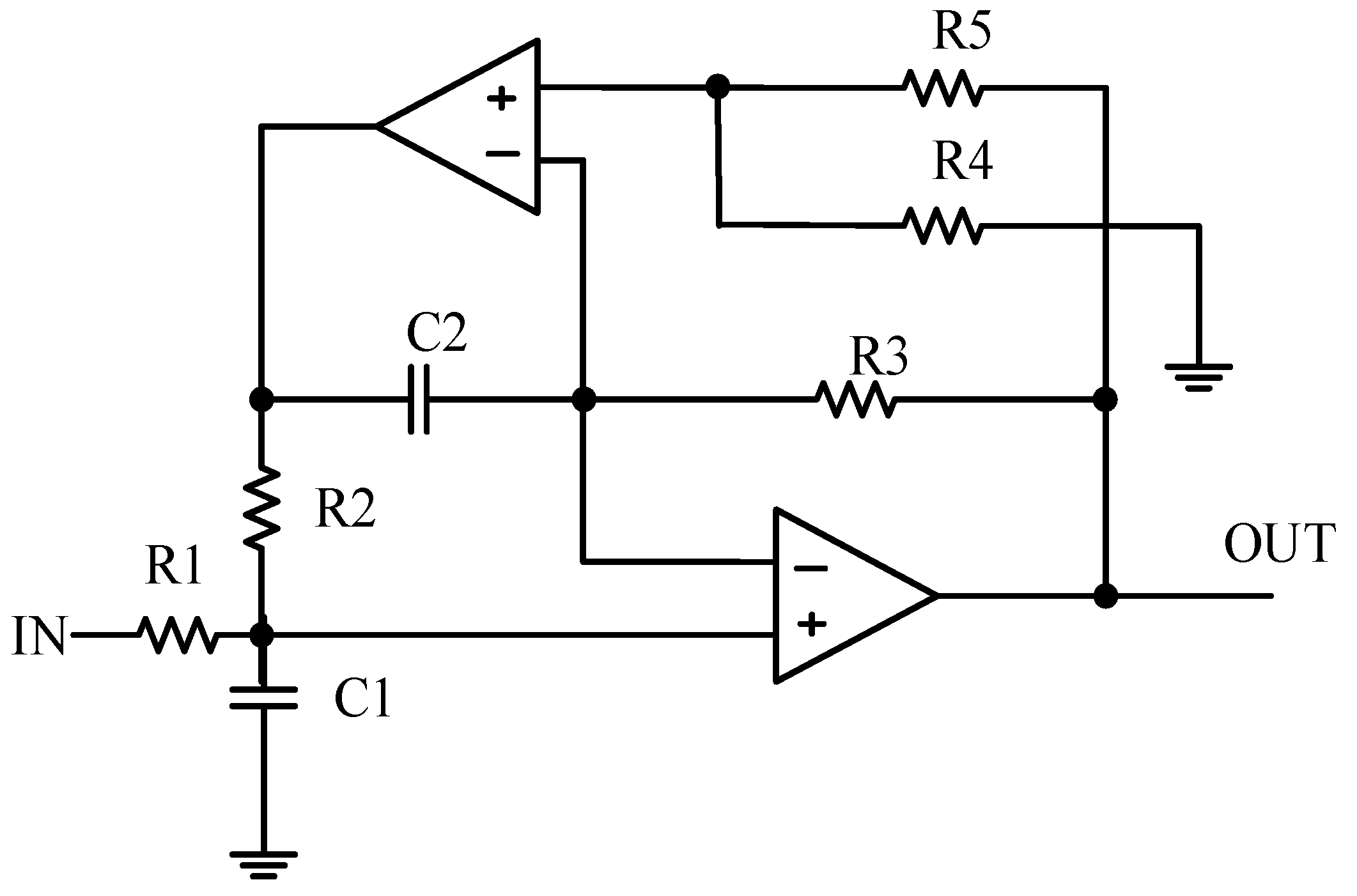
4.4. Phase Sensitive Detector Module

A phase-sensitive detector is the central component of a phase-locked amplification circuit. It multiplies the reference signal and the filtered target detection signal. Analog Devices Inc (ADI) offers the AD835, a four-quadrant analog multiplier chip with excellent multiplication gain bandwidth that fully meets the design requirements. Figure 7 shows the internal structure and pinout of this chip. In this design, pins X2 (7) and Y2 (2) are grounded. Pin Y1 (1) is connected to the output of the target signal channel, while pin X1 (6) is connected to the output of the reference signal channel. Pin W (5) is connected to the input of the low-pass filtering module, and pins VP (6) and VB (3) are connected to the positive and negative 5 V DC power supplies, respectively. Based on Equation (7), the signal passing through the phase-sensitive detector comprises a DC component and an alternating current (AC) component, with the effective signal located in the DC component. To retain the valid signal, a low-pass filter is used to remove the DC component after a multiplication operation.

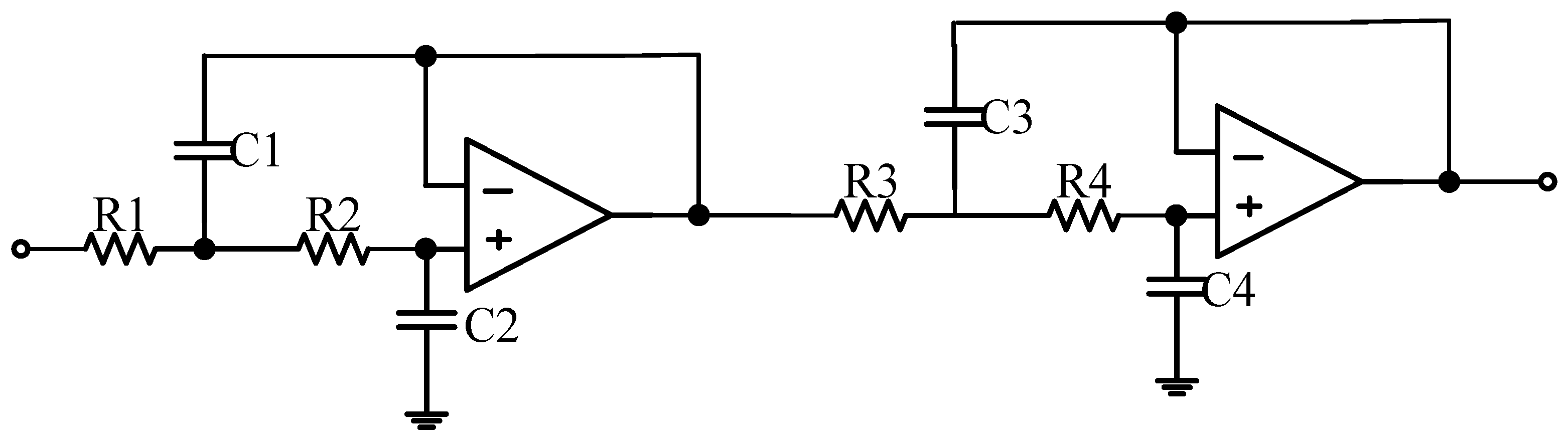
4.5. Low-Pass Filter Circuit

A low-pass filter is a type of filter that permits signals below a specific frequency to pass through. In this circuit design, the low-pass filter’s primary function is to remove the AC component resulting from the multiplication operation performed by the phase-sensitive detector, ensuring that only the DC component is preserved. This paper presents the design of a fourth-order low-pass filter using the Butterworth filter characteristic with a flat region and the Butterworth filter normalization table. The transfer function TN(s) of the Nth order low-pass filter is of the form (19), as indicated in the table.
T N s = 1 i = 1 N s s i = 1 1 + a 1 s + a 2 s 2 + a N 1 s N 1 + a N s N
Therefore, the transfer function T4(s) of the fourth-order low-pass filter is Equation (20).
T 4 s = 1 i = 1 4 s s i = 1 1 + a 1 s + a 2 s 2 + a 3 s 3 + s 4 = 1 1 + b 1 s + b 2 s 2 1 + b 3 s + b 4 s 2
The given circuit can be interpreted as two second-order low-pass filters connected in series, as shown in Figure 8. The filters have different resistance and capacitance values.
Based on its sketch, the second-order low-pass filter transfer function T ( s ) can be calculated as Equation (21).
T ( s ) = 1 R 1 R 2 C 1 C 2 s 2 + ( R 1 + R 2 ) × C 2 × s + 1
When R1 = R2 = Rf, the relationship between the cutoff frequency fc and the capacitor resistance impedance is Equation (22).
f c = 1 2 π C 1 C 2 R f
The two signals that were multiplied are passed through a fourth-order low-pass filter module to retain the DC component. The amplitude and phase values of the original target signal are then obtained by digital processing of Equations (11) and (12). Combining the above analysis of the modules of the designed circuit, we constructed a circuit suitable for processing weak signals at a target frequency of 1 MHz. In addition, the transfer function and the circuit system were thoroughly studied and analyzed in this paper.

5. Hardware Detection Circuit Debugging and Result Analysis

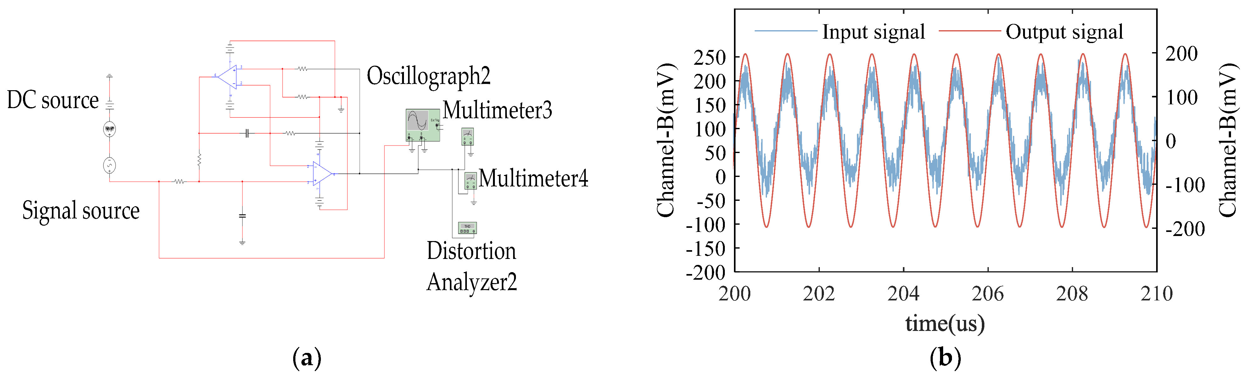
5.1. Differential Amplifier Module Testing

This section simulates the process of eliminating common mode signals by outputting the signal from the detection coil to the first module of the hardware circuit, which is the differential amplifier circuit module. The test circuit for the differential amplifier is shown in Figure 9a. The signal source produces an effective signal with an amplitude of 100 uV and a frequency of 1 MHz, while the noise source generates a white noise signal in the range of 0~1 MHz as common-mode noise. These signals simulate the output signals from the detection probe. Oscilloscope 1’s left channel (Channel-A) detects the waveforms of the input signals, while the right channel (Channel-B) detects the waveforms of the output signals. Multimeters 1 and 2 measure the AC voltage amplitude and DC offset of the output signals, respectively. Finally, distortion analyzer 1 measures the total harmonic distortion rate after differential amplification.
Figure 9b displays the results from oscilloscope 1. The blue waveform represents the input signal mixed with noise signal, while the red waveform represents the output signal after differential amplification. The period of the output signal is 996.5 ns, and the voltage amplitude is 9.945 mV. The total harmonic distortion is −62.159 dB, and the signal noise distortion is 51.746 dB. The DC bias voltage is −0.553 mV. Upon comparing the waveforms of the input and output signals, it is evident that the differential amplifier effectively amplifies the signal while filtering out the noise, thus satisfying a preamplifier’s design requirements.

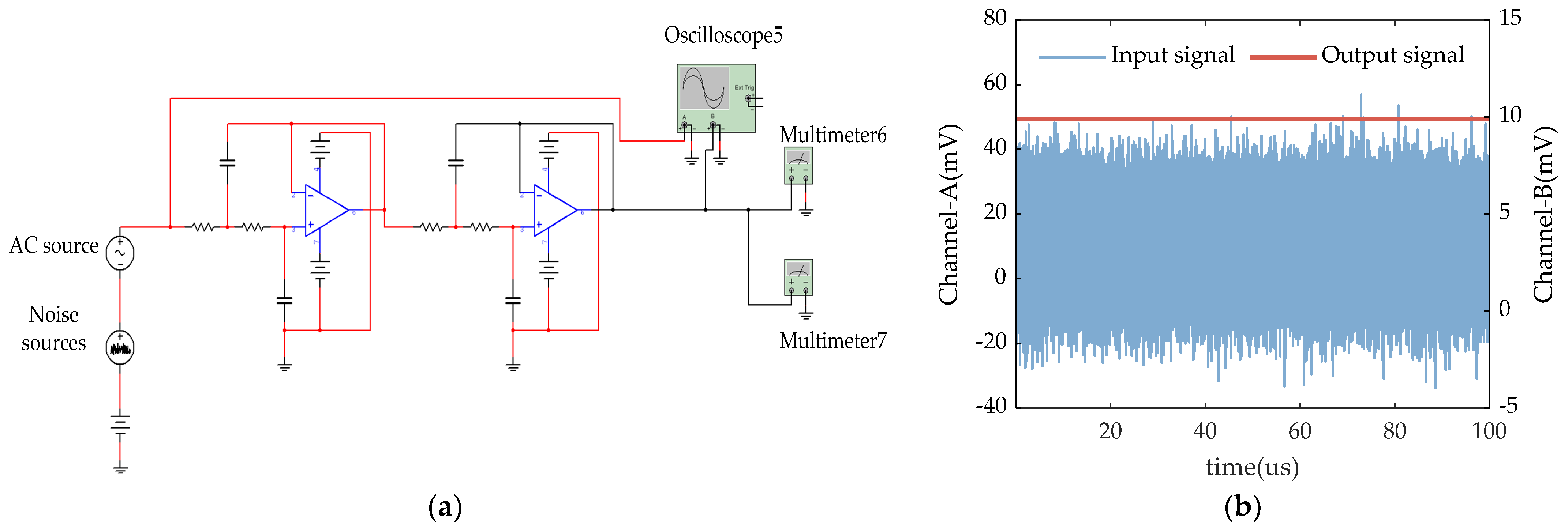
5.2. Bandpass Filter Module Testing

This section emulates the transmission of a signal through a differential amplifier module followed by its passage into a bandpass filter. The purpose of employing the bandpass filter is to retain the signal within proximity of its center frequency, thereby alleviating the burden on the multiplier chip. Figure 10a displays the band-pass filter test circuit. The signal source produces a 100 mV signal with a frequency of 1 MHz as the effective signal. The noise source generates a white noise signal ranging from 0 to 1 MHz and a DC signal of 1 mV as the noise. The experiment aims to decouple the effective 1 MHz signal using the band-pass filter. Oscilloscope 2’s left channel (Channel-A) detects the input signal waveform, while the right channel (Channel-B) detects the output signal waveform. Voltmeter 3 and voltmeter 4 measure the AC voltage amplitude and DC offset of the output signal, respectively. Distortion analyzer 2 measures the total harmonic distortion rate after the band-pass filter.
Figure 10b displays the results from oscilloscope 2. The blue waveform represents the input signal mixed with noise signal, while the red waveform represents the output signal after differential amplification. The delay response of the output signal is 140 us, and the period of the output signal is 996.5 ns. The voltage amplitude is 198.51 mV, and the total harmonic distortion is −62.889 dB. The signal noise distortion is 56.535 dB, and the DC bias voltage is −65.376 uV. The DC bias voltage is −65.376 uV. Upon comparing the waveforms of the input and output signals, it is evident that the band-pass filter amplifies the effective signal by a factor of two while filtering out the noise more effectively. This meets the design requirements of an amplifier with a band-pass filter.

5.3. Phase Shifter Module Testing

A set of harmonic signals with a phase difference of 90° is required as input to the reference channel. The raw reference signal can be generated using a signal generation module. In this section, we simulate a signal with a phase difference of 90° by passing the original reference signal through a phase shifter. These two signals, along with the original signal, are utilized as inputs to two multiplier modules. Figure 11a shows the test circuit for the phase shifter. The experiment aims to achieve a 90° phase lag for a 1 MHz input signal while maintaining the same amplitude and frequency. The input signal has an output amplitude of 100 mV. The use of clear and concise language, along with a logical flow of information, ensures that the reader can easily understand the experiment. The input signal waveform is detected using the left channel (Channel-A) of oscilloscope 3, while the right channel (Channel-B) is used to detect the output signal waveform. The total harmonic distortion rate after bandpass amplification is measured using distortion analyzer 3.
Figure 11b displays the results from oscilloscope 3. The blue waveform represents the input signal, while the red waveform represents the output signal after phase shifting. The delay response of the output signal is 1.5 us, and the period of the output signal is 998.2 ns. The voltage amplitude is 99.73 mV, and the total harmonic distortion is −51.420 dB. Upon comparing the waveforms of the input and output signals, it is evident that the phase shifter can shift the phase of the input signal by 90° while preserving the original waveform of the reference signal. This meets the design requirements of a phase shifter.

5.4. Phase Sensitive Detector Module Testing

The correlator channel serves as the central component in the overall design. This section emulates a multiplier’s functionality, where the input signal is derived from the target signal after being filtered through a bandpass filter. The reference signals utilized by the two multipliers are harmonic signals with a phase angle difference of 90 degrees. Figure 12a shows the test circuit for the phase-sensitive detector. The circuit uses a 1 MHz signal with an output amplitude of 100 mV as the signal source. The input signal is used as a reference signal, and the signal to be tested is accessed to the X and Y ends of the AD835 chip for multiplication. Oscilloscope 4’s left channel (Channel-A) detects the input signal waveform, while the right channel (Channel-B) detects the output signal waveform. The multimeter (5) measures the output DC signal magnitude, and the distortion analyzer (4) measures the harmonic distortion rate at 2 MHz after the correlator.
Figure 12b displays the results from oscilloscope 4. The blue waveform represents the input signal, while the red waveform represents the output signal after the multiplier. The delay response of the output signal is 2.5 us, and the period of the output signal is 498.2 ns. The voltage amplitude is 4.979 mV, and the DC bias voltage is 5.098 mV. The correlator meets design requirements, as it can multiply the input signal to be measured with the reference signal. The input signal was brought into Equation (6) and calculated to obtain an ideal output AC signal amplitude of 5 mV, a frequency of 2 MHz, and a DC signal output of 5 mV. The total harmonic distortion is less than −100 dB.

5.5. Low-Pass Filter Module Testing

After passing through the multiplier channel, the signal is split into an AC frequency signal and a DC signal. As previously discussed in Section 3, a low-pass filter is needed to filter out the AC signals and keep the DC signals valid for the next vector operation. In this section, the output of the multiplier module is simulated in the low-pass filter module to complete the low-pass filter circuit. Figure 13a shows the test circuit for the low-pass filter. The DC source voltage amplitude is 10 mV, and the analog multiplier amplifier output an effective DC signal. The AC source voltage amplitude is 10 mV, with a frequency of 2 MHz, and the analog multiplier amplifier output an effective AC signal. The noise source is 0~2 MHz white noise. These three signals form the input signal for the low-pass filter, from which the DC signal is obtained. The oscilloscope’s left channel (Channel-A) detects the input signal waveform, while the right channel (Channel-B) detects the output signal waveform. Multimeter 6 measures the magnitude of the output DC signal, and multimeter 7 measures the amplitude of the output AC signal.
Figure 13b shows the results displayed by oscilloscope 5, where the blue waveform is the input signal and the red waveform is the output signal after low-pass filtering. From the figure, it can be seen that after the signal passes through the low-pass filter, the high-frequency noise signals have been effectively filtered out; the amplitude of the DC signal of the output voltage is measured by a multimeter as 9.892 mV, and the low-frequency signals have been effectively retained. This low-pass filter design meets the design requirements of a correlator.

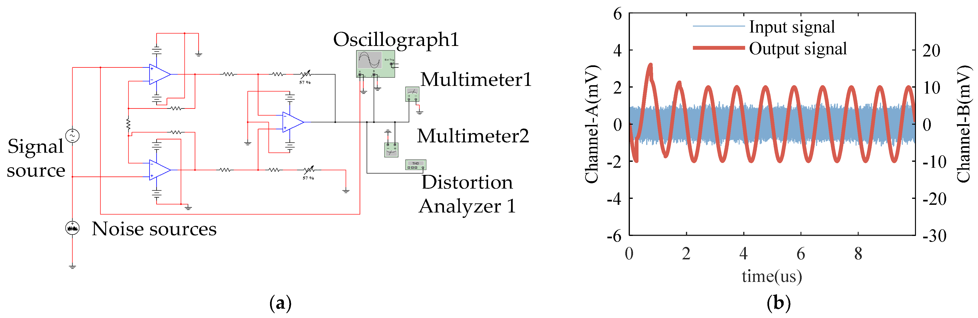
5.6. Overall Hardware Circuit Testing

In this subsection, the above modules are connected to form an overall dual-phase sensitive phase-locked amplification hardware circuit as shown in Figure 3, and Figure 14 shows its test diagram, where the amplitude of the DC component in the two-channel output signals is detected using multimeter 7 and multimeter 9, respectively, and the amplitude of the AC component in the output signals is detected using multimeter 8 and multimeter 10, respectively. To verify the performance and accuracy of the circuit in processing signals under different conditions, the reference signal is set to a 1 V, 1 MHz sinusoidal signal, and 1 MHz sinusoidal signals with different amplitudes and phases are used as valid signals and 0~1 MHz white noise signals as detection signals. The outputs of the two sets of signal amplitude, according to Equations (11) and (12) for data processing, are shown in Table 1.
The designed dual-phase sensitive phase-locked amplifier circuit, as demonstrated in Table 1, effectively extracts the 1 MHz AC signal while maintaining an amplitude error within 0.2%, resulting in a significant amplification of approximately 2000 times. By employing compensation algorithms, the measured phase angles are reduced to within 0.5% of the original fixed value of about 2.715°. Thus, our objective of extracting and amplifying a valid signal is successfully accomplished.

6. Conclusions

In this paper, we introduce a dual-phase sensitive lock-in amplifier detection circuit. Based on the lock-in amplification technique, it has a total amplification gain of 2000 times. This circuit is designed for detecting small signals from coil eddy current probes in the system. Through simulation test analysis, it is demonstrated that the signal detection circuit maintains an amplitude error below 0.2%. Furthermore, by applying a compensation algorithm and adding 2.715° to each set of phase angle detection data, phase angle error can be controlled below 0.5%. The simulation results confirm that our designed weak signal detection system accurately extracts specific frequency signals while providing high accuracy in signal amplification. This enables the effective extraction of small-impedance change signals from coil sensor probes, serving as a reliable foundation for further signal processing and analysis. In future research, this circuit can serve as a basis for developing portable probes to detect CFRP material composition and contribute to intelligent CFRP production line development. Moreover, this circuit can also be utilized for extracting eddy current detection signals from other materials.

Author Contributions

M.W., Q.X. and S.L. conceived the research idea, Q.X. and S.Z. wrote the paper; Q.X. and S.L. processed the data; Z.X. and S.C. reviewed and suggest the paper. All authors have read and agreed to the published version of the manuscript.

Funding

The paper is supported by the Shanghai Engineering Research Center of Marine Renewable Energy (Grant No. 19DZ2254800) and the Young Faculty Research Startup Fund of Shanghai Ocean University (Grant No. A2-2006-22-200320).

Institutional Review Board Statement

Not applicable.

Informed Consent Statement

Not applicable.

Data Availability Statement

The original contributions presented in the study are included in the article, further inquiries can be directed to the corresponding authors.

Conflicts of Interest

The authors declare no conflicts of interest.

References

  1. Sanai, K.; Nakasaki, S.; Hashimoto, M.; Macadre, A.; Goda, K. Fracture Behavior of a Unidirectional Carbon Fiber-Reinforced Plastic under Biaxial Tensile Loads. Materials 2024, 17, 1387. [Google Scholar] [CrossRef] [PubMed]
  2. Bogenfeld, R. Experimental Comparative Analysis of the Through-Thickness and In-Plane Compression Moduli of Unidirectional CFRP Laminates. J. Compos. Sci. 2024, 8, 76. [Google Scholar] [CrossRef]
  3. Zhou, F.; Zhang, J.; Song, S.; Yang, D.; Wang, C. Effect of Temperature on Material Properties of Carbon Fiber Reinforced Polymer (CFRP) Tendons: Experiments and Model Assessment. Materials 2019, 12, 1025. [Google Scholar] [CrossRef] [PubMed]
  4. Shuai, Y.; Li, Z.; Xuejia, Y.; Lu, L. Wandering Overview of carbon fiber 3D weaving technology and its application in new energy field. Mar. Electr. Electron. Eng. 2022, 42, 118–121. [Google Scholar] [CrossRef]
  5. Qifeng, M.; Kai, S.; Lipan, Z.; Yali, W.; Shasha, S. Study of Simulation and Experimental of a New Eddy Current Probe for Carbon Fiber Reinforced Plastics Plate. Chin. J. Sens. Actuators 2019, 32, 829–833. [Google Scholar]
  6. Wu, D.; He, T.; Wang, X.; Sun, Q. Impedance Analysis of a Meander Coil with Rectangular Cross Section above a Planar Conductor Using Vertex Description. J. Nondestruct. Eval. 2018, 37, 1–11. [Google Scholar] [CrossRef]
  7. Bouloudenine, A.; Feliachi, M.; Latreche, M.E.H. Development of circular arrayed eddy current sensor for detecting fibers orientation and in-plane fiber waviness in unidirectional CFRP. Ndt E Int. 2017, 92, 30–37. [Google Scholar] [CrossRef]
  8. Machado, M.A.; Antin, K.-N.; Rosado, L.S.; Vilaça, P.; Santos, T.G. Contactless high-speed eddy current inspection of unidirectional carbon fiber reinforced polymer. Compos. Part B Eng. 2019, 168, 226–235. [Google Scholar] [CrossRef]
  9. Daura, L.U.; Tian, G.; Yi, Q.; Sophian, A. Wireless power transfer-based eddy current non-destructive testing using a flexible printed coil array. Philos. Trans. R. Soc. A 2020, 378, 20190579. [Google Scholar] [CrossRef] [PubMed]
  10. Lefebvre, O.; Cao, H.H.; Cortés Francisco, M.; Woytasik, M.; Dufour-Gergam, E.; Ammar, M.; Martincic, E. Reusable embedded microcoils for magnetic nano-beads trapping in microfluidics: Magnetic simulation and experiments. Micromachines 2020, 11, 257. [Google Scholar] [CrossRef]
  11. Wu, D.; Cheng, F.; Yang, F.; Huang, C. Non-destructive testing for carbon-fiber-reinforced plastic (CFRP) using a novel eddy current probe. Compos. Part B Eng. 2019, 177, 107460. [Google Scholar] [CrossRef]
  12. Li, Z.; Wang, Z.; Luo, H.; Xu, Y.; Yu, J.; Jiang, Y. Weak RF Signal Detection Based on Single-Mode Optoelectronic Oscillator. IEEE Photonics Technol. Lett. 2023, 35, 313–316. [Google Scholar] [CrossRef]
  13. Li, R.; Tian, H.; Kato, T.; Asahara, A.; Minoshima, K. Broadband coherently synthesized two-color electro-optic frequency combs with phase noise suppression. Appl. Phys. Express 2022, 16, 012005. [Google Scholar] [CrossRef]
  14. Geng, X.; Ye, Z.; Xiao, Y.; Tian, Y.; Xie, Q.; Wang, Z. A 25.8-GHz integer-N CPPLL achieving 60-fs rms jitter and robust lock acquisition based on a time–amplifying phase–frequency detector. IEEE Trans. Microw. Theory Tech. 2023, 71, 4869–4881. [Google Scholar] [CrossRef]
  15. Peng, W.; Daoyu, Q.; Tianhuai, D.; Zhibin, F. Study on Signal Detection Technology of Small Inductance Planar Coil. Chinese J. Sens. Actuators 2007, 10, 2333–2336. [Google Scholar]
  16. Amenabar, I.; Mendikute, A.; López-Arraiza, A.; Lizaranzu, M.; Aurrekoetxea, J. Comparison and analysis of non-destructive testing techniques suitable for delamination inspection in wind turbine blades. Compos. Part B Eng. 2011, 42, 1298–1305. [Google Scholar] [CrossRef]
  17. Hosten, B.; Castaings, M. Comments on the ultrasonic estimation of the viscoelastic properties of anisotropic materials. Compos. Part A Appl. Sci. Manuf. 2008, 39, 1054–1058. [Google Scholar] [CrossRef]
  18. Cheng, J.; Qiu, J.; Xu, X.; Ji, H.; Takagi, T.; Uchimoto, T. Research advances in eddy current testing for maintenance of carbon fiber reinforced plastic composites. Int. J. Appl. Electromagn. Mech. 2016, 51, 261–284. [Google Scholar] [CrossRef]
  19. Shuping, Z. Simulink-based simulation analysis of weak signal detection in lock-in amplifiers. Digit. Technol. Appl. 2012, 11, 51–52+54. [Google Scholar] [CrossRef]
  20. Peng, F.; Yanan, L.; Biao, W. Simulink Simulation Design of Lock-in Amplifier for Signal Detection Theory Course. Educ. Mod. 2017, 4, 238–240. [Google Scholar] [CrossRef]
  21. Wang, G.; Reboul, S.; Choquel, J.-B.; Fertein, E.; Chen, W. Circular Regression in a Dual-Phase Lock-In Amplifier for Coherent Detection of Weak Signal. Sensors 2017, 17, 2615. [Google Scholar] [CrossRef]
Figure 1. Planar projection of figure-8 coils.
Applsci 14 03618 g001
Figure 2. Single-turn current loop.
Applsci 14 03618 g002
Figure 3. Schematic diagram of a dual-phase sensitive lock-in amplifier.
Applsci 14 03618 g003
Figure 4. Schematic diagram of differential amplifier.
Applsci 14 03618 g004
Figure 5. Schematic diagram of bandpass filter.
Applsci 14 03618 g005
Figure 6. Structure diagram of phase shifter.
Applsci 14 03618 g006
Figure 7. Internal schematic and pins of AD835.
Applsci 14 03618 g007
Figure 8. Schematic diagram of second-order low-pass filter.
Applsci 14 03618 g008
Figure 9. Modeling of differential amplification module. (a) Circuit of differential amplifier, (b) input/output waveform of differential amplification circuit signal.
Applsci 14 03618 g009
Figure 10. Modeling of bandpass filter module. (a) Circuit of bandpass filter, (b) Input and output waveforms of bandpass filter circuits.
Applsci 14 03618 g010
Figure 11. Modeling of phase shifter module. (a) Circuit of phase sensitive detector, (b) output waveform of phase sensitive detectors.
Applsci 14 03618 g011
Figure 12. Modeling of phase sensitive detector module. (a) Circuit of phase sensitive detector module testing. (b) Input and output waveform of phase sensitive detectors.
Applsci 14 03618 g012
Figure 13. Modeling of low pass filter module testing. (a) Circuit of low pass filter, (b) Input and output waveforms of low-pass filters.
Applsci 14 03618 g013
Figure 14. Modeling of overall hardware circuit testing.
Applsci 14 03618 g014
Table 1. Input and output signal data sheets.
Amplitude (I)Phase (I)Output 1Output 2Amplitude Calculation ResultsPhase Calculation ResultsAmplitude ErrorPhase Error
10 uV30°−4.496 mV−8.915 mV19.969 mV27.389°0.155%0.345%
10 uV54°−7.828 mV−6.219 mV19.995 mV51.534°0.025%0.459%
50 uV72°−46.808 mV−17.825 mV100.174 mV69.153°0.174%0.184%
70 uV−40°47.566 mV−51.497 mV140.207 mV−42.7278°0.147%0.032%
100 uV−98.610 mV5.518 mV200.249 mV−2.7195°0.124%0.45%
100 uV26°−39.413 mV−92.045 mV200.257 mV23.180°0.128%0.405%
Disclaimer/Publisher’s Note: The statements, opinions and data contained in all publications are solely those of the individual author(s) and contributor(s) and not of MDPI and/or the editor(s). MDPI and/or the editor(s) disclaim responsibility for any injury to people or property resulting from any ideas, methods, instructions or products referred to in the content.

