Article

Electroless Copper Patterning on TiO2-Functionalized Mica for Flexible Electronics

by
Bozhidar I. Stefanov
1,*,
Boriana R. Tzaneva
1,*,
Valentin M. Mateev
2 and
Ivo T. Iliev
3
1
Department of Chemistry, Faculty of Electronic Engineering and Technology, Technical University of Sofia, Kliment Ohridski Blvd., 8, 1000 Sofia, Bulgaria
2
Department of Electrical Apparatus, Faculty of Electrical Engineering, Technical University of Sofia, Kliment Ohridski Blvd., 8, 1000 Sofia, Bulgaria
3
Department of Electronics, Faculty of Electronic Engineering and Technology, Technical University of Sofia, Kliment Ohridski Blvd., 8, 1000 Sofia, Bulgaria
*
Authors to whom correspondence should be addressed.
Appl. Sci. 2024, 14(21), 9780; https://doi.org/10.3390/app14219780
Submission received: 25 September 2024 / Revised: 17 October 2024 / Accepted: 24 October 2024 / Published: 25 October 2024
(This article belongs to the Section Chemical and Molecular Sciences)

Abstract

:

Featured Application

The technology presented in this work enables the fabrication of conductive patterns on flexible mica substrates through its functionalization with TiO2. This approach allows for the photocatalytic patterning of electroless copper deposition Ag-based catalyst, which facilitates a versatile and scalable route for creating conductive layers on flexible inorganic substrates, making it suitable for applications in electronics and, as demonstrated, sensing device fabrications.

Abstract

The formation of conductive copper patterns on mica holds promise for developing cost-effective flexible electronics and sensing devices, though it is challenging due to the low adhesion of mica’s atomically flat surface. Herein, we present a wet-chemical method for copper patterning on flexible mica substrates via electroless copper deposition (Cu-ELD). The process involves pre-functionalizing 50 µm thick muscovite mica with a titanium dioxide (TiO2) layer, via a sol–gel dip-coating method with a titanium acetylacetonate-based sol. Photolithography is employed to selectively activate the TiO2-coated mica substrates for Cu-ELD, utilizing in situ photodeposited silver (Ag) nanoclusters as a catalyst. Copper is subsequently plated using a formaldehyde-based Cu-ELD bath, with the duration of deposition primarily determining the thickness and electrical properties of the copper layer. Conductive Cu layers with thicknesses in the 70–130 nm range were formed within 1–2 min of deposition, exhibiting an inverse relationship between plating time and sheet resistance, which ranged from 600 to 300 mΩ/sq. The electrochemical thickening of these layers to 1 μm further reduced the sheet resistance to 27 mΩ/sq. Finally, the potential of Cu-ELD patterning on TiO2-functionalized mica for creating functional sensing devices was demonstrated by fabricating a functional resistance temperature detector (RTD) on the titania surface.

1. Introduction

The increasing integration of electronics into everyday life demands new material characteristics, e.g., developing sensory systems like piezo-sensors, flexible solar power sources, and wearable health-monitoring sensors requires flexible substrates [1,2,3,4]. Many organic materials, such as polymer films (PET, PEN, PI, and PC) [5] and flexible porous materials like paper, textiles, electrospun nanofibers, wood, and elastic polymer sponges [6], have been studied for this application. However, their primary drawback is their low thermal resistance, limiting their use when higher temperatures are required during both processing and operation.
Inorganic materials, on the other hand, enable operation at elevated temperatures. The strong covalent, metallic, or ionic bonds give them high elasticity moduli and minimal deformation before fracture, making them suitable for flexible electronics. Examples include glass, silicon wafers, perovskite materials, and thin metal foils. These substrates, when thinned, offer bendability, thermal resistance, dimensional stability, and, in some cases, transparency, making them ideal for flexible solar powered devices [1,7]. Mica is another example of a temperature-resistant, transparent, and flexible substrate. It provides excellent insulation, chemical stability, and thermal resistance [8,9] and has been explored as a substrate for growing functional oxides [8,9,10,11,12]. However, as a silicate material, mica faces challenges in adhesion with conductive layers, which can be improved by surface roughening or using adhesion-promoting sublayers [13,14,15,16].
Conductive layers on mica are generally deposited as conducting oxides [8,17], metallic transition metal dichalcogenides [18], and, less frequently, metals [14]. Various techniques, such as sol–gel spin-coating [10], magnetron sputtering [11], pulsed laser deposition (PLD) [12,17], molecular beam epitaxy [19], PVD, and CVD [18,20], have been used to deposit such layers on mica. Despite its advantages, such as room temperature processing and cost-effectiveness, electroless metal deposition on mica is rarely reported [14]. Electroless metal plating is an autocatalytic process where conductive layers may be formed on any dielectric surface, preactivated with a catalyst, from an electrolyte containing metal ions, a reducing agent, and stabilizers. This method is commonly used for forming conductive copper layers in the electronics industry and the production of printed circuit boards, in particular. Electroless copper deposition technology can produce high-purity Cu layers suitable for forming vias and interconnects in the ultra-large-scale integration (ULSI) of integrated circuits [21,22,23]. One of the key advantages of electroless Cu deposition is its room temperature process, which helps avoid impurities like the undesirable oxide phases associated with Cu2O. These phases can poison the copper, leading to poor ductility and reduced electrical properties in smelted copper [24]. Electroless Cu deposition can achieve extremely high-purity Cu layers with an oxygen content as low as 74 ppm, meeting the standards for oxygen-free high-conductivity (OFHC) copper [25]. However, the most common impurity in electroless copper films is embedded hydrogen, typically originating from the gas released by the formaldehyde-based reducing agent used in the process [22,23]. Dissolved oxygen in the plating bath might also be embedded, especially at lower deposition rates [26].
The main challenge with silicate materials, such as mica, is modifying the surface to improve adhesion and deposit a catalyst for the reaction [16]. Palladium (Pd) and platinum (Pt) are the most commonly used catalysts for electroless copper reactions with formaldehyde as the reducing agent [16,27,28]. However, the literature has shown that cost-effective alternative catalysts, such as highly dispersed silver (Ag) and copper (Cu) nanoparticles, can also effectively activate the electroless Cu deposition process [29,30].
In recent studies, we demonstrated a method for selective photocatalytic activation and chemical metallization by functionalizing the surface with a thin TiO2 layer. This approach was applied to anodic aluminum oxide (AAO) substrates [31] and glass substrates to fabricate functional humidity sensors based on the TiO2 layer properties [32]. The method provides good adhesion to insulating substrates like glass and anodized aluminum oxide. It also allows the direct additive patterning of conductive images by UV irradiation through a mask in a solution of metal ions, such as Cu2+ and Ag+. However, this approach’s limitation is the need for a high-temperature annealing step (450–500 °C) to form the TiO2 layer by sol–gel coating, thus restricting its use to silicate or ceramic materials. Mica, with its excellent thermal, mechanical, and chemical stability, is a promising substrate to employ this functionalization route, while simultaneously offering mechanical flexibility.
This study aims to explore the selective deposition of conductive copper patterns on functionalized mica substrates via electroless copper deposition (Cu-ELD). Unlike previous work focusing on the photocatalytic activation of the TiO2-functionalized substrate or its use as an active sensing material, this research investigates how the Cu-ELD process parameters affects the electrical properties of the copper layers. Understanding these effects could allow for the controlled modulation of copper layer conductivity, a feature with potential for the development of resistance temperature detectors (RTDs). Given copper’s high temperature coefficient of resistance, this makes it well suited for RTD applications, despite the limitations of copper’s low intrinsic resistivity. Demonstrating functional RTD devices based on Cu-ELD copper layers is also a key goal of this study.

2. Materials and Methods

2.1. Reagents

Electronic grade mica sheets (14 mm × 50 mm × 0.05 mm condenser mica plates) were used as substrates, obtained from Pasat Electronics Ltd. (Gorna Oryahovitza, Bulgaria). Titanium tetraisopropoxide (TTIP, 97+%), acetylacetone (AcAc, 99%), and silver nitrate (AgNO3, ACS, 99.9+%) were sourced from Alfa Aesar (Ward Hill, MA, USA). Isopropyl alcohol (2-propanol, ≥99.8%, HPLC grade) was supplied by Avantor (Radnor, PA, USA). Copper sulfate pentahydrate (CuSO4·5H2O, 98+%, for analysis) and ethylenediaminetetraacetic acid (EDTA, ACS, ≥99.0%) were supplied by Thermo Scientific (Waltham, MA, USA).

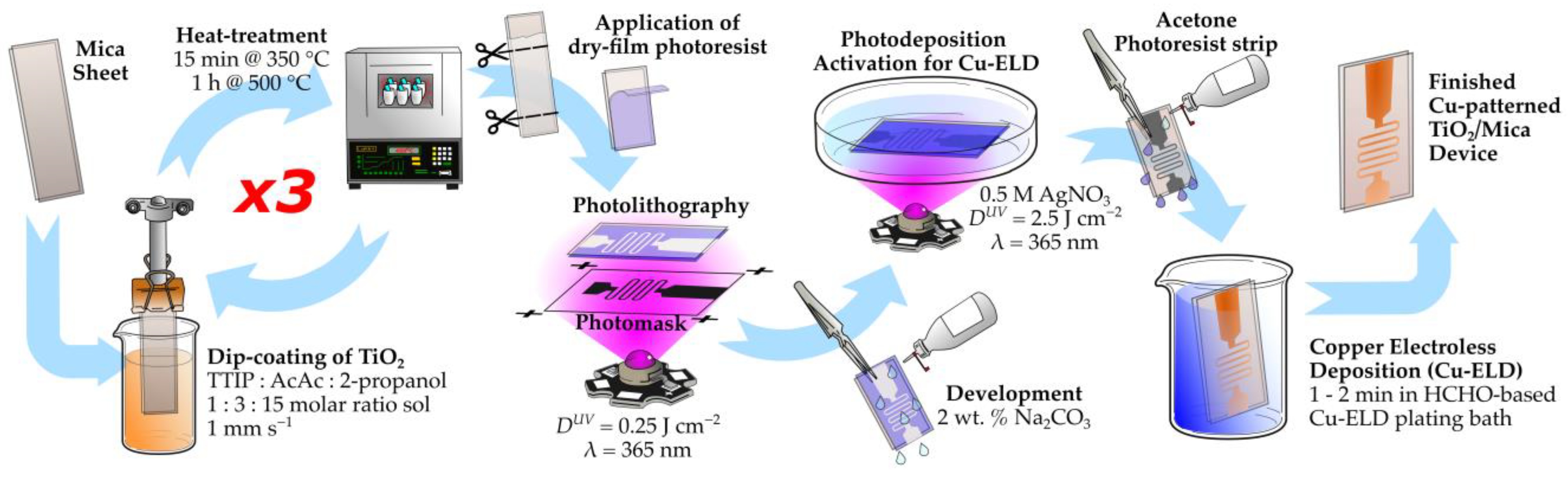
2.2. Preparation of TiO2-Coated Mica Substrates

Natural mica sheets (14 mm × 50 mm × 0.05 mm) were used as substrates. The sheets were degreased using 2-propanol and subsequently coated with TiO2 via sol–gel dip-coating. The sol was composed of TTIP, AcAc, and 2-propanol in a 1:3:15 molar ratio. The detailed preparation and characterization of this sol have been previously published [32].
The dip-coating process was performed using a custom-built apparatus, with a withdrawal rate of 1 mm s−1. Three coating cycles were applied, each followed by heat treatment at 350 °C for 15 min and 500 °C for 1 h. The mass change in the TiO2-coated mica was measured gravimetrically, yielding an average of 14.6 ± 1.3 μg cm−2 per cycle, resulting in a total mass of 43.9 ± 2.6 μg cm−2 after the third cycle (n = 20 samples). Assuming a TiO2 layer density of 3.9 g cm−3, the estimated film thickness was approximately 112 nm.

2.3. Copper Patterning and Device Fabrication on TiO2-Coated Mica Substrates

The prepared TiO2-coated mica substrates were used for Cu electroless deposition (Cu-ELD), as shown schematically in Figure 1.
To activate the substrates for Cu-ELD, Ag was photodeposited as a catalyst by exposing the substrate to UV light in an aqueous 0.5 M AgNO3 solution. A volume of 0.15 mL of the Ag+ solution was spread onto the surface of a Petri dish, with the TiO2-coated mica substrate placed on top. The UV illumination was provided from beneath using a UV LED (LTPL-C034UVH365, λ = 365 ± 5 nm, LiteOn Optoelectronics, Taipei, Taiwan). The UV irradiation intensity at the TiO2 surface was measured at 16.7 mW cm−2 using a calibrated optical power meter (Thorlabs PM400 with S175C thermopile detector, Thorlabs, Newton, NJ, USA). Samples were exposed for 2.5 min to achieve a total UV dose (DUV) of 2.5 J cm−2. After photodeposition, the Ag-activated TiO2/Mica substrates were rinsed with distilled water, dried with hot air, and immersed into the Cu-ELD bath.
The Cu-ELD bath comprised 18 g L−1 CuSO4·5H2O, 48 g L−1 EDTA, 57 mg L−1 concentrated HCl, and 48 mL L−1 37% aqueous formaldehyde (HCHO). The pH of the solution was adjusted to 12.3 using 5 M NaOH. Cu-ELD was performed for 1–2 min on Ag-activated TiO2/Mica substrates, resulting in the immediate darkening of the Ag-activated areas and the formation of pink Cu layers. Depositions longer than 3 min caused the bubbling and delamination of the copper layer, while those shorter than 1 min resulted in non-conductive layers.
This method was further applied to study the feasibility of using the Cu-ELD layers in resistance temperature detectors (RTDs). RTD devices were fabricated using selective Ag activation to create a serpentine pattern on the TiO2/Mica surface. The serpentine design consisted of a 300 μm wide copper track with six loops, 1 mm pitch, 8 mm lateral width, and a total length of 55 mm, which is shown in Figure 2a. A 40 μm thick dry-film negative photoresist was laminated on the substrate and exposed through a photomask at a UV dose of 0.25 J cm−2. The photoresist was developed in 2 wt.% Na2CO2, followed by Ag activation and Cu-ELD, as described earlier. Prior to the Cu deposition, the photoresist was stripped using acetone. Figure 2b presents a photographic image of a finished Cu-ELD serpentine pattern, deposited on mica.

2.4. Characterization Methods

Surface morphology was observed using a TESCAN Lyra I XMU scanning electron microscope (SEM) (Brno, Czechia) operating at 20 kV. Atomic force microscopy (AFM) was performed using a Nanosurf FlexAFM (Liestal, Switzerland). Energy-dispersive X-ray (EDX) analysis was conducted using a Quantax 200 EDX detector (Bruker Nano GmbH, Berlin, Germany) coupled to the SEM. Raman spectroscopy was performed using a TO-ERS-532 spectrometer (Thunder Optics, Montpellier, France) with a 532 nm laser source and a ×20 objective. UV/Vis transmittance spectra were measured using a SP-V1100 spectrometer (DLAB Scientific Co., Ltd., Beijing, China). X-ray diffraction (XRD) patterns were collected using a D8 Advance diffractometer (Bruker AXS GmbH, Karlsruhe, Germany) with a CuKα source and LynxEye PSD detector. The sheet resistance of the samples was measured using a Veeco FPP-5000 four-point probe (Veeco Instruments Inc., Plainview, NY, USA).

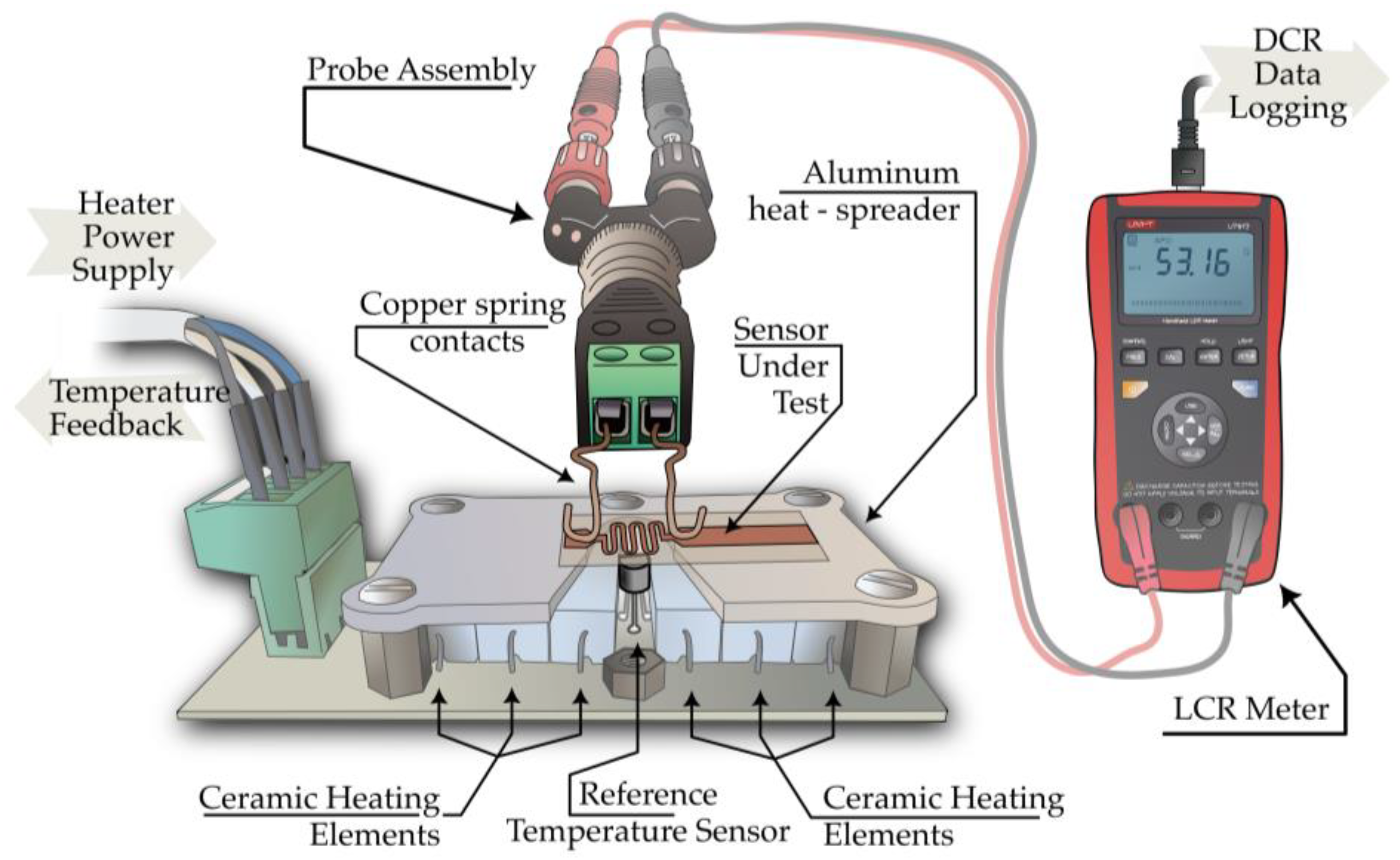
2.5. Determination of Temperature Sensing Response

The RTD performance of the Cu-ELD layers in serpentine geometries was tested using a custom setup shown in Figure 3.
The sensor was placed on a temperature-controlled heating bed composed of six ceramic resistors (18 Ω, 5 W) arranged in parallel beneath an aluminum heat spreader (65 mm × 40 mm × 3 mm). A DS18B20 digital temperature sensor (Maxim Integrated, San Jose, CA, USA) embedded in the heat spreader provided feedback to an Arduino Nano microcontroller (Arduino SRL, Torino, Italy), programmed to maintain a temperature range of 30–65 °C. The temperature stability at each setpoint was ±0.14 °C, with heating ramp rates of 2.78 ± 0.34 °C min−1 across the range. Resistance measurements were taken in situ using a 2-wire probe connected to the RTD’s copper contact pads, monitored via a UT-612 LCR meter (Uni-Trend Tech. Co., Ltd., Dongguan, China) in direct-current resistance (DCR) mode with a resolution of 0.01Ω.

3. Results and Discussion

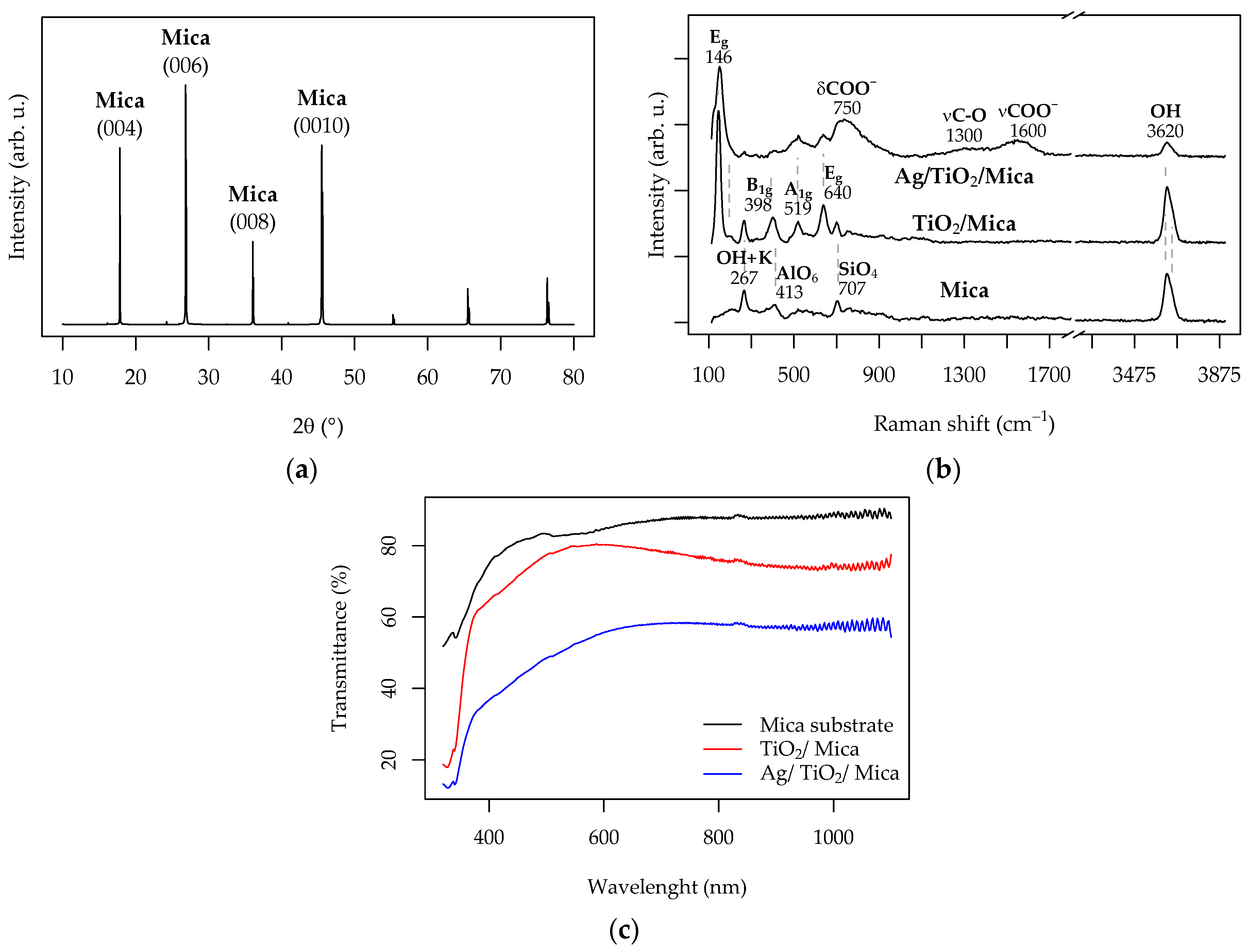
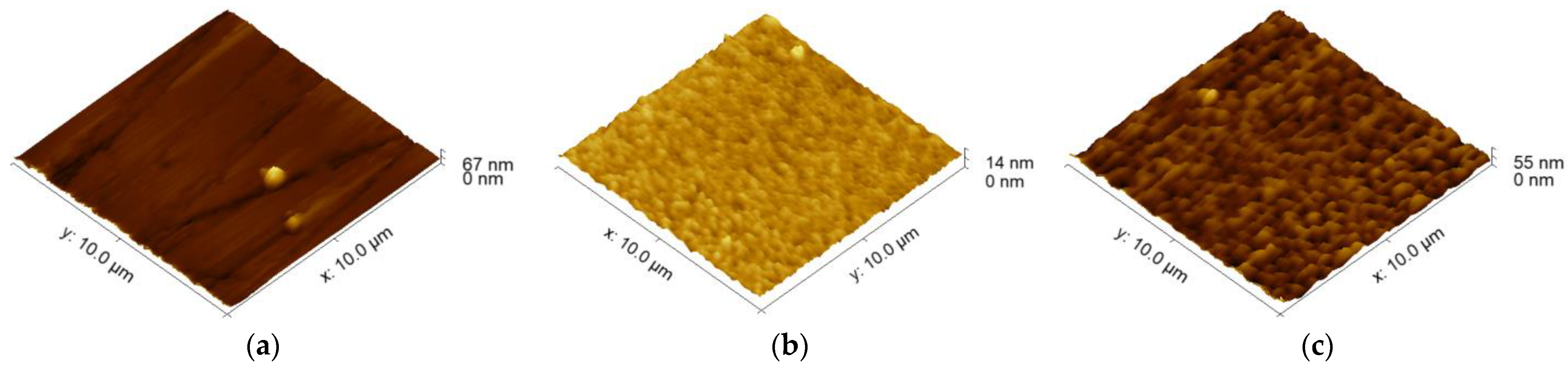
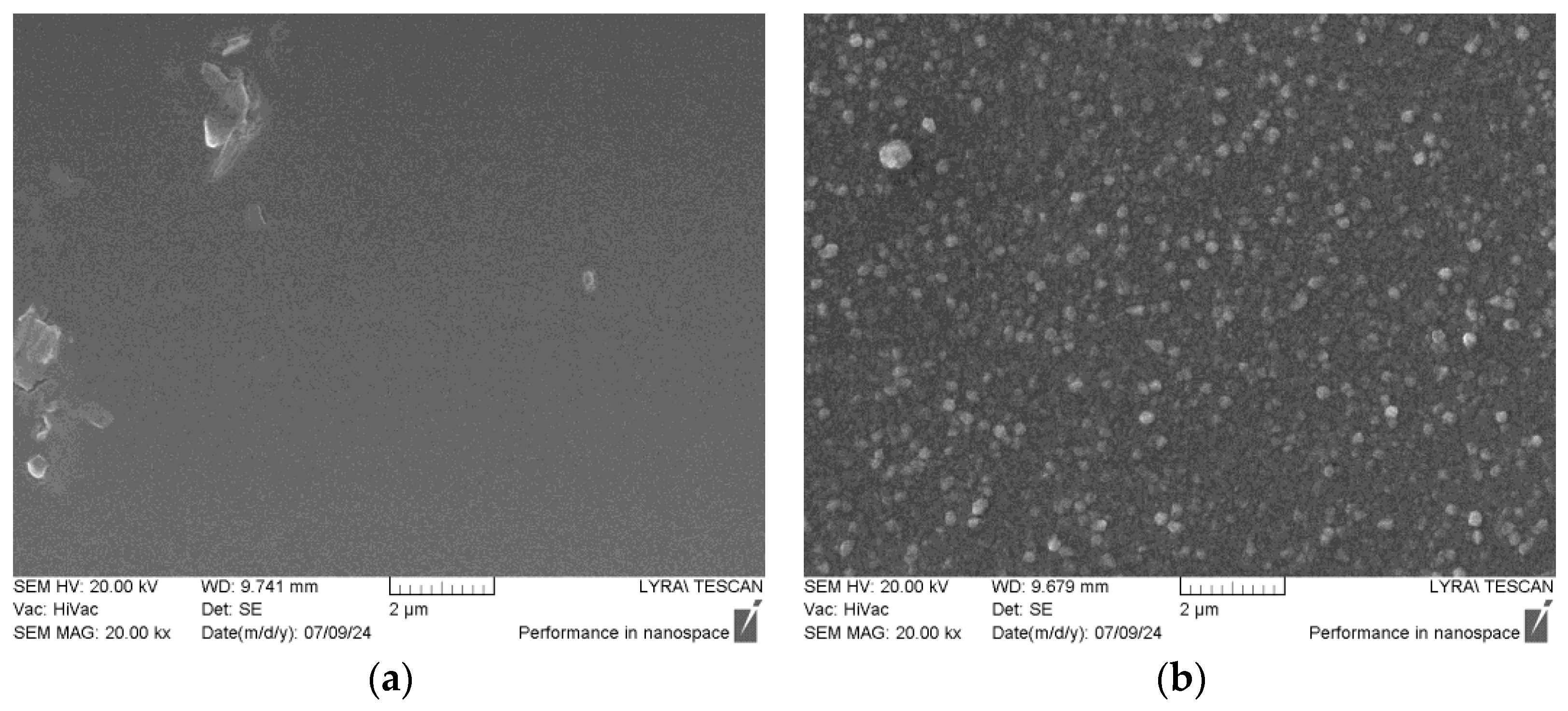
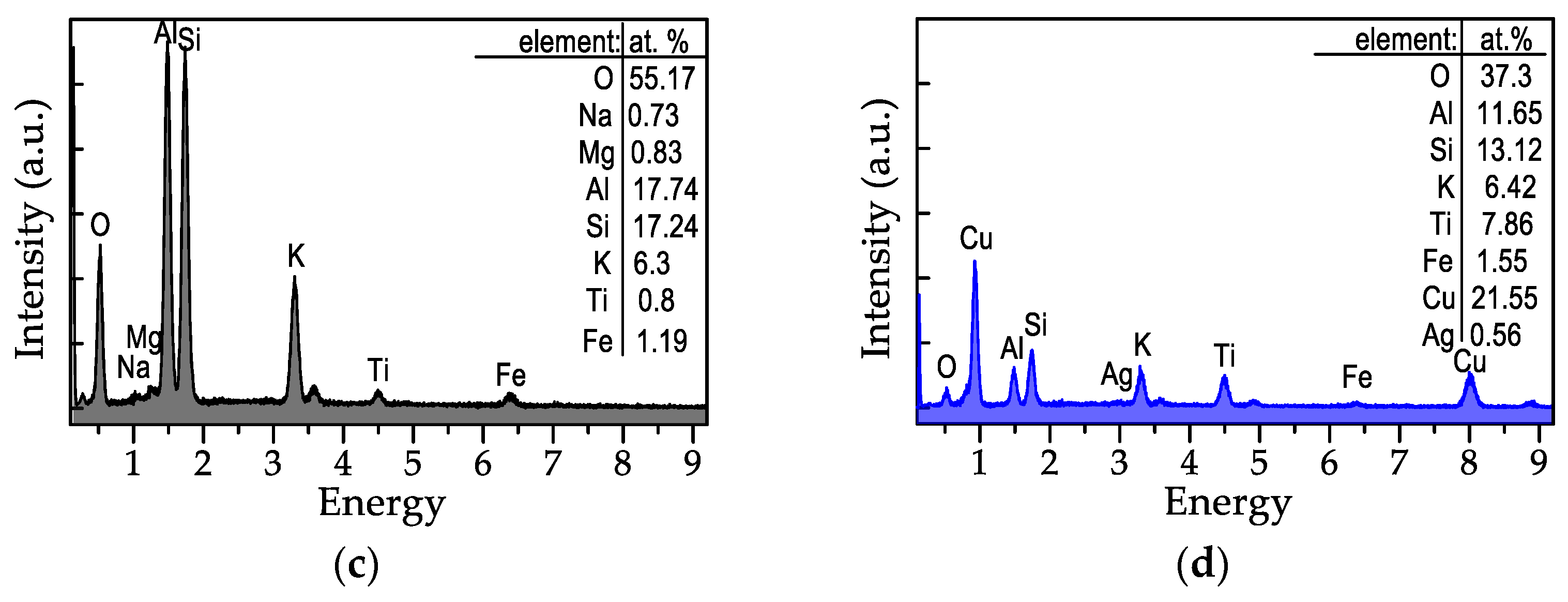
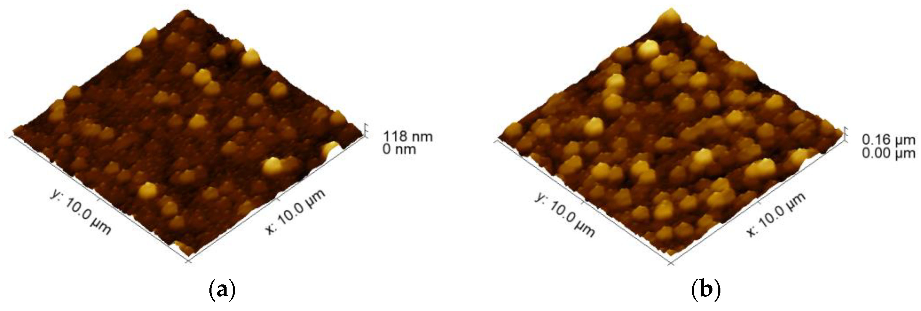
3.1. Characterization of the TiO2-Functionalized Mica Substrates

The TiO2-functionalized mica substrates were characterized using XRD, with a representative diffraction pattern shown in Figure 4a. The XRD patterns of the pristine and TiO2-coated substrates, both before and after Ag activation at 2.5 J cm−2, were identical. These patterns were dominated by strong reflections from the mica substrate, observed at 17.8°, 26.9°, 36°, and 45.5° 2θ, corresponding to the (002), (004), (008), and (0010) planes of Muscovite 2M1 (KAl2(Si,Al)4O10(OH)2, PDF#00-058-2034) [33,34]. The intense reflections from the substrate made the detection of the functional TiO2 layer impossible via XRD. Therefore, Raman spectroscopy was employed to investigate the phase composition of the TiO2 layer.
Figure 4b displays Raman scattering spectra for the starting mica substrate, the TiO2/mica functionalized substrate, and the TiO2/mica substrate after Ag photodeposition. The Raman spectrum of the mica substrate is characterized by distinct bands in the low-frequency region at 267 cm−1, 413 cm−1, and 707 cm−1, corresponding to the lattice O-H-O + K vibrations, the Al-O modes of AlO6 octahedra, and the Si-O modes of the SiO4 tetrahedra, respectively [35]. Additionally, a pronounced asymmetric peak in the high-frequency hydroxyl region centered at 3620 cm−1, with a shoulder at 3650 cm−1, is attributed to Si-OH modes, consistent with muscovite in agreement with the XRD evidence [36].
The TiO2 functionalization is evident in the Raman spectrum of the TiO2/mica sample, which shows the appearance of the Eg (146 cm−1, 640 cm−1), B1g (398 cm−1), and A1g (519 cm−1) modes associated with anatase TiO2 [37]. Although the XRD patterns did not change after Ag photodeposition, the Raman spectra did. As shown in Figure 4b, two main changes occurred. First, there was a strong suppression of the anatase A1g and B1g modes, which became broader and weaker, indicative of a significant electronic interaction between the photodeposited Ag and the TiO2 surface. This effect is commonly observed in photodeposited metals [38] and is likely due to the sensitivity of these modes to surface changes and stress [39]. Additionally, the Ag/TiO2/mica spectrum exhibited new spectral features, including broad peaks centered around 750 cm−1, 1300 cm−1, and 1600 cm−1. These peaks, which have been observed in the Raman spectra of Ag nanoparticles, can be attributed to various δCOO, νC-O, and νCOO/νC=O modes of surface-bound carbonaceous species, coming from exposure to air, intensified via surface-enhanced Raman scattering (SERS) effects caused by the Ag clusters [40,41].
The optical transparency of the mica substrate, which may be advantageous for applications such as photodetector fabrication, was assessed using UV/Vis transmittance spectra (Figure 4c). The pristine muscovite substrate exhibited high transparency across the entire spectral range, with only a 10% reduction after TiO2 functionalization, most pronounced at λ < 380 nm due to absorption below the TiO2 bandgap. The Ag/TiO2/mica sample activated for Cu-ELD patterning became noticeably darker due to the presence of finely dispersed Ag particles, as seen in Figure 4c.
Surface morphology was investigated using AFM imaging, with representative images shown in Figure 5. The pristine mica surface (Figure 5a) had a smooth but slightly terraced morphology, possibly due to the imperfect cleavage of the technical-grade mica substrate. The root-mean-square (RMS) roughness (Rq) was found to be 3.87 nm. After TiO2 functionalization, the surface appeared smoother (Rq = 0.94 nm), and the polycrystalline anatase layer consisted of spherical grains with diameters under 100 nm (Figure 5b). After Ag photodeposition (Figure 5c), the surface coarsened, increasing the Rq to 5.12 nm.

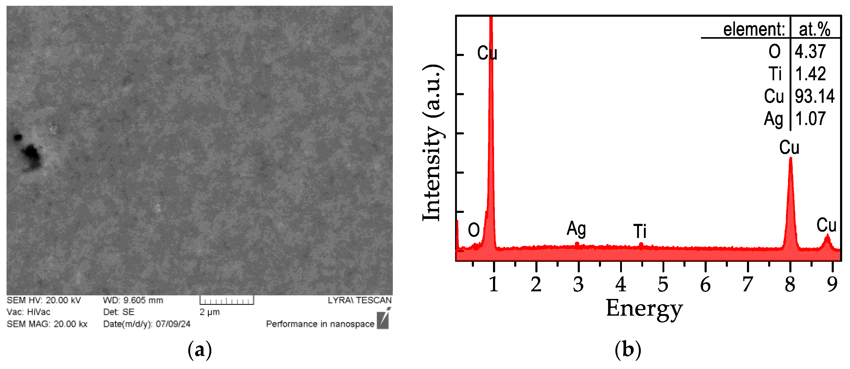
3.2. Electroless Copper Deposition on Ag-Activated TiO2/Mica Substrates

The morphology and structure of copper layers formed via electroless deposition (Cu-ELD) on Ag-activated TiO2/Mica substrates were examined using SEM and AFM imaging. In all cases, the activation dose (DUV) for the silver catalyst was 2.5 J cm−2, and the only parameter varied was the duration of the Cu-ELD process, with plating times of 1, 1.5, and 2 min. Figure 6 shows SEM images of the TiO2/mica substrate before (Figure 6a) and after Ag activation and 2 min of Cu-ELD (Figure 6b).
The composition results, obtained via EDX measurements, are displayed in Figure 6c,d, respectively. Initially, the pristine TiO2/Mica substrate exhibited a uniform, flat morphology, and the EDX analysis aligned well with the expected chemical composition of Muscovite 2M1 (KAl2(Si,Al)4O10(OH)2). However, trace amounts of Mg and Fe (≈1 at.%) were detected, which is not unexpected for naturally sourced, technical-grade mica [36]. The surface-deposited TiO2 was also detectable at 0.8 at.%, although the thinness of the layer and the high penetrability of the 20 kV electron beam likely contributed to this low value.
The Cu-ELD layer formed after 2 min of plating (Figure 6b) comprised flat, roughly spherical copper domains which were 50–100 nm in diameter. After Cu-ELD, copper became the dominant element in the EDX analysis (Figure 6d). The presence of both Ti and Ag from the Ag/TiO2/Mica underlayer also became more apparent due to the surface sensitivity of the measurement, enhanced by copper’s electron stopping power.
Additional AFM analysis was conducted to investigate the effects of the Cu-ELD duration on copper layer morphology. As shown in Figure 7a,b, which present AFM images of copper layers formed after 1 and 2 min of electroless deposition, there were no significant differences in morphology, with both layers exhibiting relatively flat copper domains of roughly spherical symmetry. However, increased coarseness was observed in the copper layer deposited for a longer time, corroborated by the root-mean-square (RMS) roughness measurements, where Rq increased from 13.64 nm to 23.23 nm.
The phase composition of the Cu-ELD layer was further studied using XRD. Despite the dominance of mica reflection peaks in the Ag/TiO2/mica patterns (viz. Figure 4a), metallic copper was identifiable through the distinct Cu (111) reflection at 43.4° 2θ (PDF#03-065-9026). Figure 8 presents a close-up of this region in the XRD pattern for Cu-ELD layers formed on TiO2/Mica for 1, 1.5, and 2 min. The results clearly show that longer Cu-ELD durations led to an increase in the intensity of the Cu (111) peak, as the copper layer thickness increased. The mean crystallite sizes, determined from the FWHM of the Cu (111) peak using the Scherrer equation, were 38.3 nm, 39.1 nm, and 39.4 nm, respectively. This indicates that the layers are polycrystalline, with the domain-like features observed in SEM and AFM images consisting of multiple Cu grains, and that the plating duration had little effect on the crystallite size.
The substantial growth in Cu layer thickness during the 1–2 min of Cu-ELD was further confirmed by AFM microscopy, performed on the serpentine track topology (see Figure 2). Figure 9a–c shows AFM images at the interface between the Cu-ELD coated track and the uncoated TiO2/Mica substrate, with markers indicating the areas used to determine the height cross-section plots shown in Figure 9d–f.
These data revealed that the Cu track heights were 71 nm, 106 nm, and 132 nm for the Cu-ELD layers grown over 1, 1.5, and 2 min, respectively. Although based on a limited dataset, these results suggest a linear growth rate for Cu-ELD layers of approximately 68 nm min−1.
Finally, the effect of the Cu-ELD plating duration on the electrical conductivity of the copper layers was evaluated. Table 1 summarizes the data for the sheet resistance (Rs) versus Cu-ELD duration and AFM-measured thickness (d) for the three layers formed during the 1–2 min of Cu deposition. As expected, the increased thickness led to a corresponding decrease in Rs. The specific resistivity (ρ) of the Cu-ELD layers, calculated using ρ = d × Rs, was found to be 4.32 ± 0.21 μΩ cm−1, which is about 2.5 times higher than the bulk Cu value (ρ∞ = 1.7 μΩ cm−1) but is still within an acceptable range for ~100 nm thick Cu-ELD layers, where values below 5 μΩ cm−1 are considered a benchmark and typical values for such layers can often exceed 12–300 μΩ cm−1 [42,43].

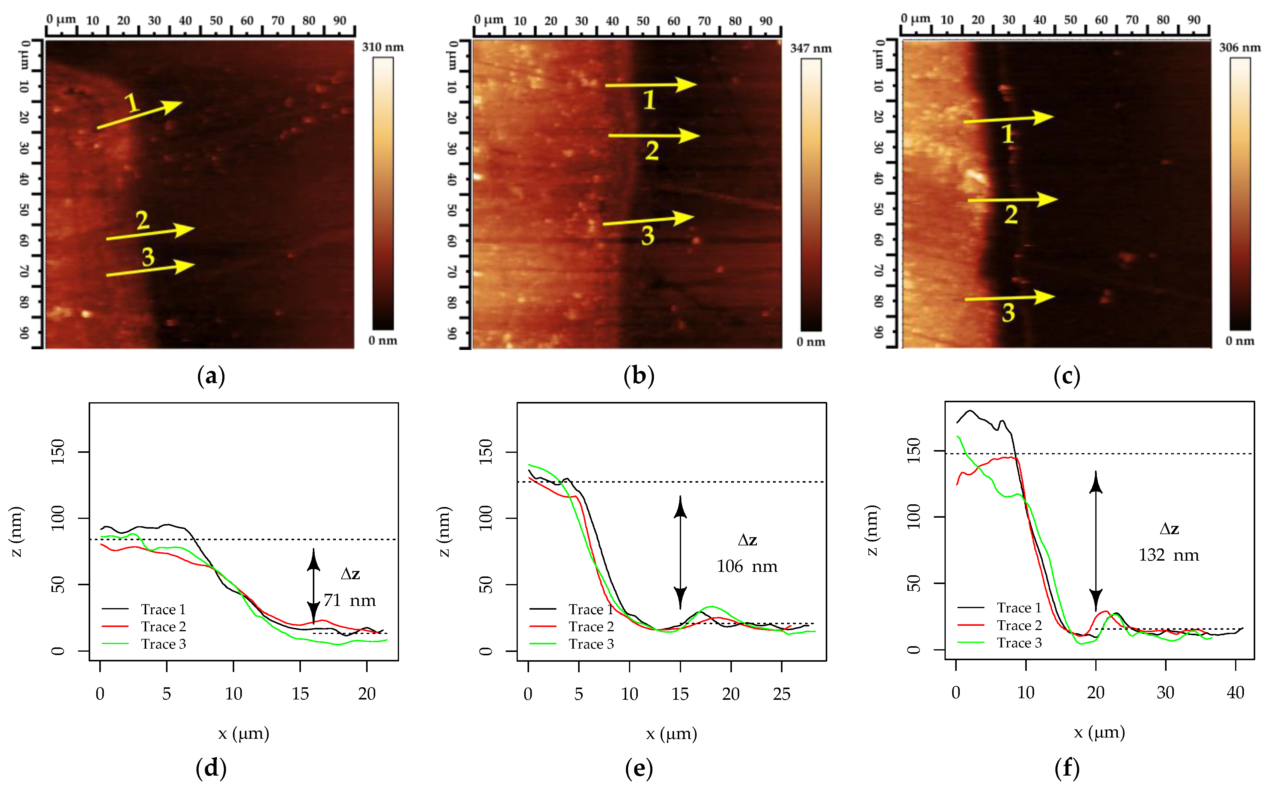
3.3. Thickening of Cu-ELD Layers by Copper Electroplating

While the wet-chemical Cu-patterning of mica substrates yields layers with excellent conductivity compared to typical thin Cu-ELD layers, the relatively high resistivity of electroless copper layers may present challenges for practical applications requiring higher current-handling capacities. This is particularly important for the fabrication of functional mica-based PCBs. As discussed earlier, extending Cu-ELD durations beyond 3 min often led to the bubbling and delamination of the copper layer in this study. An industrially favored solution for enhancing the electrical conductivity of electrolessly deposited layers on dielectric surfaces is to use electrochemical plating to thicken the layers to the desired thickness.
In this study, we also explored this approach by thickening the Cu-ELD layer through electrochemical copper deposition. Ag-activated TiO2/Mica substrates with a 2 min Cu-ELD coating were further plated in a two-electrode electrochemical copper plating bath. The anode was a 99.9% copper plate, and the electrolyte contained 200 g L−1 CuSO4·5H2O, 50 g L−1 concentrated H2SO4, and 50 mg L−1 NaCl. The current density at the Cu-ELD cathode was set to 10 mA cm−2, and the plating duration was 10 min, resulting in an additional 1 μm of copper being deposited.
As shown in Figure 10a, the electroplated copper layer exhibited a dense, highly uniform morphology. Correspondingly, the EDX spectrum (Figure 10b) revealed that copper was the predominant element detected, and the Ti-K, O-K, and Ag-K peaks coming from the substrate are highly attenuated by the thicker copper layer, while the other elements K-peaks associated with the substrate (Al, Si, K, and Fe) become unobservable. The sheet resistance of the electrochemically thickened copper layer was measured to be an order of magnitude lower than the best-case Cu-ELD scenario, at 27 ± 3 mΩ/sq.

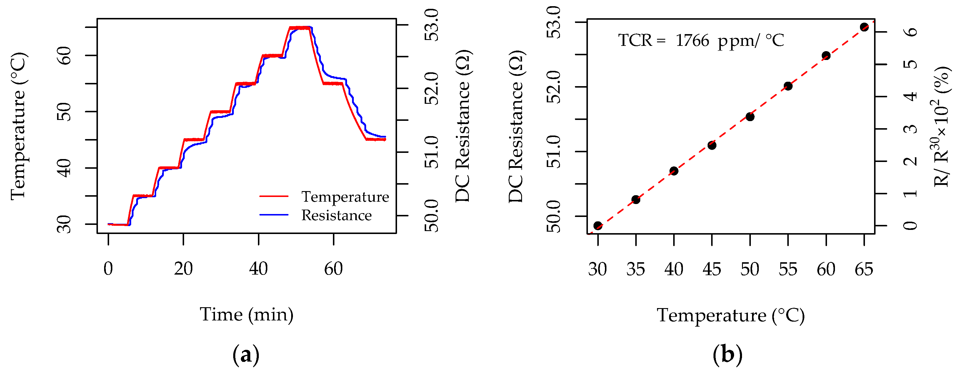
3.4. Functional Resistance-Temperature Detector Sensors on Cu-ELD Patterned TiO2/Mica Substrates

As demonstrated in the previous subsections, the Cu-ELD patterning route on TiO2-functionalized mica allows for a relatively straightforward control of the Cu-layer thickness by adjusting the electroless deposition time. Given the relatively high resistivity of the ≈100 nm thick Cu-ELD layers, combined with the possibility of spatially selective patterning via photolithography (see Figure 1), one of the main objectives of this study was to explore the applicability of the Cu-ELD patterns as resistance temperature detectors (RTDs). The experiments were conducted on Cu-ELD layers with a serpentine RTD geometry (see Figure 2). Devices were fabricated with varied Cu-ELD durations in the 1–2 min range, and the temperature-dependent direct current resistance (DCR) was measured.
Figure 11a shows a typical result, illustrating the resistance change in a Cu-ELD serpentine pattern deposited for 2 min in the electroless deposition bath. The temperature response was measured in 5 °C increments between 30 and 65 °C, with each temperature step held for 5 min. The results show a strong correlation between the substrate’s temperature and the measured resistance across the serpentine, which is the fundamental operating principle of RTD-type temperature sensors.
The temperature response of RTDs is typically quantified by calculating the temperature coefficient of resistance (TCR). Figure 11b shows the functional dependence of DCR on temperature. The DCR value, obtained after stabilization at the end of each 5 min heating step, is plotted against the corresponding temperature, revealing a linear correlation and an overall 6% change in resistance for this particular RTD pattern. The resistance–temperature dependence could be defined as R(T) = R0 × (1 + TCR × T), where R30 is the initial resistance, measured at 30 °C; thus, the TCR can be derived from the slope of the plot R(T)/R30 − 1 vs. T. In the example in Figure 11b, the change is expressed in percentage; however, TCR values are commonly reported in ppm/°C. Experiments were performed in triplicate for the three Cu-ELD cases discussed previously, fabricated with 1, 1.5, and 2 min electroless deposition durations, and two additional samples were included for validation, fabricated with 1.25 and 1.75 min durations. The electroplating-thickened Cu-ELD layers from Section 3.3 were excluded due to their low initial DCR (~0.7 Ω), which resulted in RTD changes below the 0.01 Ω resolution of the LCR meter.
The general trends in the RTD properties of the Cu-ELD layers, as influenced by electroless deposition time, are shown in Figure 12, along a summary of all of the numerical data, which is presented in Table 2. The DCR at a fixed temperature decreased exponentially with the increasing Cu-ELD duration, from 670 Ω to 50 Ω for deposition times between 1 and 2 min (Figure 12a). This behavior, which aligns with the AFM-measured thickness range of 71–131 nm, is consistent with exponential resistance increases observed in the literature for even vacuum-deposited copper layers [44]. The absolute change in resistance from 30 °C to 65 °C (ΔR) was roughly proportional to the initial resistance R30, as shown in Figure 12b. This suggests that thinner Cu layers, which have higher intrinsic resistance, exhibit larger measurable changes in resistance, potentially making their readout easier in practical applications. However, this linear relationship does not perfectly correspond to the estimated TCR values, which increased from 995 to 1800 ppm °C−1 with increasing Cu-ELD durations and layer thicknesses. Even the best-case TCR was about 50% lower than the literature value for metallic copper (3930 ppm °C−1) [45], likely due to the influence of the photodeposited Ag catalyst, which generally has a lower TCR than copper, especially in thinner Cu layers.

4. Conclusions

In this work, we demonstrated the use of electroless copper deposition (Cu-ELD) for forming conductive copper patterns on muscovite mica using a wet-chemical process. The pre-functionalization of mica with a TiO2 layer allowed the selective activation of the mica surface with a photodeposited Ag catalyst for Cu-ELD patterning, which is also adaptable to other inorganic substrates.
At a fixed photodeposition-activation UV dose, the Cu-ELD deposition time was the primary factor influencing the thickness, morphology, and electrical properties of the conductive copper patterns formed. Conductive layers with a thickness of 70–130 nm formed within 1–2 min, with the sheet resistance decreasing from 600 to 300 mΩ/sq. as the plating time increased. Thickening these layers to 1 μm by electrochemical plating further reduced sheet resistance to 27 mΩ/sq. These tunable-thickness Cu-ELD layers, formed in a serpentine sensor topology, were employed as functional resistance temperature detector (RTD) elements, with the deposition time reducing the intrinsic resistance from 670 Ω to 50 Ω. The temperature coefficient of resistance (TCR) for the as-fabricated patterns ranged from 995 to 1800 ppm °C−1, increasing with layer thickness.
The flexibility of Cu-ELD as a wet-chemical approach, when combined with TiO2-functionalization and Ag photodeposition activation, highlights its potential for fabricating electronic and sensing devices on flexible substrates like mica. The RTD sensors fabricated in this study may also be fine-tuned for use as low-cost, disposable sensors in biomedical applications, given their sensitivity within the body temperature range. Future work should explore alternative catalysts to minimize the impact on the TCR and investigate mica’s substrate flexibility effects on Cu-ELD layers for tensiometric sensor applications.

Author Contributions

Conceptualization, B.I.S., B.R.T. and I.T.I.; methodology, B.I.S. and B.R.T.; investigation, B.I.S., B.R.T. and V.M.M.; data curation, B.I.S., B.R.T. and V.M.M.; formal analysis, B.I.S., B.R.T., V.M.M. and I.T.I.; writing—original draft preparation, B.I.S. and B.R.T.; writing—review and editing, B.I.S., B.R.T., V.M.M. and I.T.I.; visualization, B.I.S., B.R.T. and V.M.M.; supervision, funding acquisition, and project administration, I.T.I. All authors have read and agreed to the published version of the manuscript.

Funding

This study is financed by the European Union NextGenerationEU through the National Recovery and Resilience Plan of the Republic of Bulgaria, project No. BG-RRP-2.004-0005 “Improving the research capacity and quality for international recognition and sustainability of TU-Sofia”.

Institutional Review Board Statement

Not applicable.

Informed Consent Statement

Not applicable.

Data Availability Statement

The original contributions presented in the study are included in the article, further inquiries can be directed to the corresponding author.

Conflicts of Interest

The authors declare no conflicts of interest.

References

  1. Hu, X.; Huang, Z.; Zhou, X.; Li, P.; Wang, Y.; Huang, Z.; Su, M.; Ren, W.; Li, F.; Li, M.; et al. Wearable large-scale perovskite solar-power source via nanocellular scaffold. Adv. Mater. 2017, 29, 1703236. [Google Scholar] [CrossRef] [PubMed]
  2. Wang, K.N.; Li, Z.Z.; Cai, Z.M.; Cao, L.M.; Zhong, N.N.; Liu, B.; Zhou, K.; Huo, F.Y.; Cai, B.; Bu, L.L. The applications of flexible electronics in dental, oral, and craniofacial medicine. NPJ Flex. Electron. 2024, 8, 33. [Google Scholar] [CrossRef]
  3. Li, H.; Ma, Y.; Huang, Y. Material innovation and mechanics design for substrates and encapsulation of flexible electronics: A review. Mater. Horiz. 2021, 8, 383–400. [Google Scholar] [CrossRef] [PubMed]
  4. Hussain, A.M.; Hussain, M.M. CMOS-technology-enabled flexible and stretchable electronics for internet of everything applications. Adv. Mater. 2016, 28, 4219–4249. [Google Scholar] [CrossRef]
  5. Lee, S.; Reuveny, A.; Reeder, J.; Lee, S.; Jin, H.; Liu, Q.; Yokota, T.; Sekitani, T.; Isoyama, T.; Abe, Y.; et al. A transparent bending-insensitive pressure sensor. Nat. Nanotechnol. 2016, 11, 472–478. [Google Scholar] [CrossRef]
  6. Zhang, Y.; Zhang, T.; Huang, Z.; Yang, J. A new class of electronic devices based on flexible porous substrates. Adv. Sci. 2022, 9, 2105084. [Google Scholar] [CrossRef]
  7. Song, F.; Zheng, D.; Feng, J.; Liu, J.; Ye, T.; Li, Z.; Wang, K.; Liu, S.; Yang, D. Mechanical durability and flexibility in perovskite photovoltaics: Advancements and applications. Adv. Mater. 2024, 36, 2312041. [Google Scholar] [CrossRef]
  8. Bitla, Y.; Chu, Y.H. MICAtronics: A new platform for flexible X-tronics. FlatChem 2017, 3, 26–42. [Google Scholar] [CrossRef]
  9. Bitla, Y.; Chu, Y.H. van der Waals oxide heteroepitaxy for soft transparent electronics. Nanoscale 2020, 12, 18523–18544. [Google Scholar] [CrossRef]
  10. Kim, D.Y.; Lee, S.; Lin, Z.H.; Choi, K.H.; Doo, S.G.; Chang, H.; Leem, J.Y.; Wang, Z.L.; Kim, S.O. High temperature processed ZnO nanorods using flexible and transparent mica substrates for dye-sensitized solar cells and piezoelectric nanogenerators. Nano Energy 2014, 9, 101–111. [Google Scholar] [CrossRef]
  11. Li, M.; Wang, Y.; Wang, Y.; Wei, X. AZO/Ag/AZO transparent flexible electrodes on mica substrates for high temperature application. Ceram. Int. 2017, 43, 15442–15446. [Google Scholar] [CrossRef]
  12. Liu, J. High-performance orthorhombic correlated transparent conducting epilayer integrated on a flexible mica substrate: The case of CaMoO3. Ceram. Int. 2024, 50, 22149–22158. [Google Scholar] [CrossRef]
  13. Ulapane, S.B.; Doolin, J.L.; Okeowo, M.K.; Berrie, C.L. Atomic force microscopy-based static plowing lithography using CaCO3 nanoparticle resist layers as a substrate-flexible selective metal deposition resist. J. Phys. Chem. C 2021, 125, 23490–23500. [Google Scholar] [CrossRef]
  14. Liu, W.; Qiao, X.; Liu, S.; Shi, S.; Liang, K.; Tang, L. A new process for pre-treatment of electroless copper plating on the surface of mica powders with ultrasonic and nano-nickel. J. Alloys Compd. 2019, 791, 613–620. [Google Scholar] [CrossRef]
  15. Schneider, M.; Möhwald, H.; Akari, S. Quantitative measurement of chromium’s ability to promote adhesion. J. Adhes. 2003, 79, 597–607. [Google Scholar] [CrossRef]
  16. Su, W.; Yao, L.; Yang, F.; Li, P.; Chen, J.; Liang, L. Electroless plating of copper on surface-modified glass substrate. Appl. Surf. Sci. 2011, 257, 8067–8071. [Google Scholar] [CrossRef]
  17. Liu, J. Manganese-doped transparent conductive magnetic indium oxide films integrated on flexible mica substrates with high mechanical durability. Ceram. Int. 2022, 48, 3390–3396. [Google Scholar] [CrossRef]
  18. Huan, Y.; Shi, J.; Zhao, G.; Yan, X.; Zhang, Y. 2D metallic transitional metal dichalcogenides for electrochemical hydrogen evolution. Energy Technol. 2019, 7, 1801025. [Google Scholar] [CrossRef]
  19. Schouteden, K.; Amin-Ahmadi, B.; Li, Z.; Muzychenko, D.; Schryvers, D.; Van Haesendonck, C. Electronically decoupled stacking fault tetrahedra embedded in Au (111) films. Nat. Commun. 2016, 7, 14001. [Google Scholar] [CrossRef]
  20. Zhou, S.; Gan, L.; Wang, D.; Li, H.; Zhai, T. Space-confined vapor deposition synthesis of two dimensional materials. Nano Res. 2018, 11, 2909–2931. [Google Scholar] [CrossRef]
  21. Hsu, H.-H.; Lin, K.-H.; Lin, S.-J.; Yeh, J.-W. Electroless Copper Deposition for Ultralarge-Scale Integration. J. Electrochem. Soc. 2000, 148, C47. [Google Scholar] [CrossRef]
  22. Shacham-Diamand, Y.; Dubin, V.; Angyal, M. Electroless copper deposition for ULSI. Thin Solid Film. 1995, 262, 93–103. [Google Scholar] [CrossRef]
  23. Pawar, K.; Dixit, P. A critical review of copper electroless deposition on glass substrates for microsystems packaging applications. Surf. Eng. 2022, 38, 576–617. [Google Scholar] [CrossRef]
  24. Zasadzińska, M.; Knych, T.; Smyrak, B.; Strezępek, P. Investigation of the Dendritic Structure Influence on the Electrical and Mechanical Properties Diversification of the Continuously Casted Copper Strand. Materials 2020, 13, 5513. [Google Scholar] [CrossRef] [PubMed]
  25. Pedraza, A.J.; Godbole, M.J. Recrystallization and mechanical properties of electroless copper. I. Scr. Metall. Mater. 1990, 24, 1185–1189. [Google Scholar] [CrossRef]
  26. Oita, M.; Matsuoka, M.; Iwakura, C. Deposition rate and morphology of electroless copper film from solutions containing 2,2′-dipyridyl. Electrochim. Acta 1997, 42, 1435–1440. [Google Scholar] [CrossRef]
  27. Ghosh, S. Electroless copper deposition: A critical review. Thin Solid Film. 2019, 669, 641–658. [Google Scholar] [CrossRef]
  28. Bindra, P.; White, J.R. Ch. 12. Fundamental aspects of electroless copper plating. In Electroless Plating: Fundamentals and Applications; Mallory, G.O., Hajdu, J.B., Eds.; William Andrew: Norwich, NY, USA, 1990; pp. 289–329. [Google Scholar]
  29. Zhang, Y.; Zhang, T.; Shi, H.; Liu, Q.; Wang, T. Fabrication of flexible copper patterns by electroless plating with copper nanoparticles as seeds. Appl. Surf. Sci. 2021, 547, 149220. [Google Scholar] [CrossRef]
  30. Wang, X.; Ma, W.; Cai, Z. Colloidal Silver Activation for Electroless Copper Deposition. Surf. Eng. Appl. Electrochem. 2023, 59, 467–472. [Google Scholar] [CrossRef]
  31. Stefanov, B.I.; Milusheva, V.S.; Kolev, H.G.; Tzaneva, B.R. Photocatalytic activation of TiO2-functionalized anodic aluminium oxide for electroless copper deposition. Catal. Sci. Technol. 2022, 12, 7027–7037. [Google Scholar] [CrossRef]
  32. Stefanov, B.I. Wet-Chemical Fabrication of Functional Humidity Sensors on a TiO2-Coated Glass Substrate via UV Photodeposition. Coatings 2024, 14, 795. [Google Scholar] [CrossRef]
  33. Rashed, M.N.; Arifien, A.E.; El-Dowy, F.A. Preparation and characterization of nanomuscovite by intercalation method for adsorption of heavy metals from polluted water. Environ. Geochem. Health 2023, 45, 5127–5144. [Google Scholar] [CrossRef] [PubMed]
  34. Liang, J.J.; Hawthorne, F.C. Rietveld refinement of micaceous materials; muscovite-2M 1, a comparison with single-crystal structure refinement. Canad. Mineral. 1996, 34, 115–122. [Google Scholar]
  35. Wang, H.; Sun, Y.; Chu, J.; Wang, X.; Zhang, M. Intensive study on structure transformation of muscovite single crystal under high-dose γ-ray irradiation and mechanism speculation. R. Soc. Open Sci. 2019, 6, 190594. [Google Scholar] [CrossRef]
  36. Li, H.; Zhang, L.; Christy, A.G. The correlation between Raman spectra and the mineral composition of muscovite and phengite. In Ultrahigh-Pressure Metamorphism; Dobrzhinetskaya, L.F., Faryad, S.W., Wallis, S., Cuthbert, S., Eds.; Elsevier: Amsterdam, The Netherlands, 2011; pp. 187–212. [Google Scholar] [CrossRef]
  37. Zhang, W.F.; He, Y.L.; Zhang, M.S.; Yin, Z.; Chen, Q. Raman scattering study on anatase TiO2 nanocrystals. J. Phys. D 2000, 33, 912. [Google Scholar] [CrossRef]
  38. Melvin, A.A.; Illath, K.; Das, T.; Raja, T.; Bhattacharyya, S.; Gopinath, C.S. M–Au/TiO2 (M= Ag, Pd, and Pt) nanophotocatalyst for overall solar water splitting: Role of interfaces. Nanoscale 2015, 7, 13477–13488. [Google Scholar] [CrossRef]
  39. Shirpay, A.; Tavakoli, M. The behavior of the active modes of the anatase phase of TiO2 at high temperatures by Raman scattering spectroscopy. Indian J. Phys. 2022, 96, 1673–1681. [Google Scholar] [CrossRef]
  40. Joshi, N.; Jain, N.; Pathak, A.; Singh, J.; Prasad, R.; Upadhyaya, C.P. Biosynthesis of silver nanoparticles using Carissa carandas berries and its potential antibacterial activities. J. Sol-Gel Sci. Technol. 2018, 86, 682–689. [Google Scholar] [CrossRef]
  41. Shan, W.; Liu, R.; Zhao, H.; He, Z.; Lai, Y.; Li, S.; He, G.; Liu, J. In situ surface-enhanced Raman spectroscopic evidence on the origin of selectivity in CO2 electrocatalytic reduction. ACS Nano 2020, 14, 11363–11372. [Google Scholar] [CrossRef]
  42. Radoeva, M.; Radoev, B. Ohm resistivity of electroless copper layers as a function of their thicknesses. J. Mater. Sci. 1995, 30, 2215–2219. [Google Scholar] [CrossRef]
  43. Glickman, E.; Inberg, A.; Fishelson, N.; Shaham-Diamand, Y. Electroless deposition and electrical resistivity of sub-100 nm Cu films on SAMs: State of the art. Microelectron. Eng. 2007, 84, 2466–2470. [Google Scholar] [CrossRef]
  44. Schmiedl, E.; Wissmann, P.; Finzel, H.U. The electrical resistivity of ultra-thin copper films. Z. Für Naturforschung A 2008, 63, 739–744. [Google Scholar] [CrossRef]
  45. Eargle, J.M. Resistance Change with Temperature for Copper. In Electroacoustical Reference Data; Springer US: Boston, MA, USA, 1994; pp. 106–107. [Google Scholar] [CrossRef]
Figure 1. Schematic of the TiO2-functionalization, Ag photodeposition activation patterning, and Cu electroless deposition procedure.
Applsci 14 09780 g001
Figure 2. Images presenting: (a) schematic of the RTD serpentine topology; (b) photographic image of the resulting Cu-ELD fabricated RTD device.
Applsci 14 09780 g002
Figure 3. Schematic representation of the temperature-controlled heater setup used in RTD-property determination experiments.
Applsci 14 09780 g003
Figure 4. Characterization of the Ag/TiO2/mica substrates used for Cu-ELD: (a) A representative XRD pattern showing diffraction peaks from the mica substrate; (b) Raman spectra; and (c) UV/Vis transmittance spectra of the pristine, TiO2-functionalized, and Ag-activated substrates (photodeposition DUV of 2.5 J cm−2 in all cases).
Applsci 14 09780 g004
Figure 5. AFM images of the substrates, at a 10 × 10 μm field of view, at different stages of surface treatment: (a) pristine mica surface; (b) TiO2-functionalized mica surface; (c) TiO2/Mica surface after photodeposition of Ag at DUV of 2.5 J cm−2.
Applsci 14 09780 g005
Figure 6. SEM images and EDX spectra of the samples: (a,c) TiO2/Mica substrate; (b,d) Cu-ELD layer after 2 min on Ag/TiO2/Mica substrate.
Applsci 14 09780 g006aApplsci 14 09780 g006b
Figure 7. AFM topography images, at a 10 × 10 μm field of view, for the Cu-ELD layer formed after: (a) 1 min and (b) 2 min of Cu-ELD plating. Both layers were deposited on Ag/TiO2/Mica substrates activated with DUV of 2.5 J cm−2.
Applsci 14 09780 g007
Figure 8. XRD data showing the Cu (111) reflection, consistent with metallic Cu, for Cu-ELD layers grown on the Ag/TiO2/mica substrate after 1, 1.5, and 2 min of deposition.
Applsci 14 09780 g008
Figure 9. AFM topography images at (ac) a 100 × 100 μm field of view, and corresponding cross-section plots (df) for determining Cu-ELD layer thickness after (a,d) 1 min, (b,e) 1.5 min, and (c,f) 2 min in the Cu-ELD bath. The plots, displayed in panes (df), are obtained according to the position and scan direction indicated via yellow arrows in panes (ac).
Applsci 14 09780 g009
Figure 10. SEM-EDX analysis of a Cu layer (2 min Cu-ELD), thickened to 1 μm via electrochemical Cu plating: (a) SEM surface morphology; (b) EDX spectrum.
Applsci 14 09780 g010
Figure 11. Representative data showing the performance of Cu-ELD patterns as resistance temperature detectors for a Cu-ELD serpentine pattern developed on a TiO2/Mica substrate during 2 min of electroless deposition: (a) raw data showing the correlation between temperature and direct current resistance; (b) processed data showing the functional dependence used to estimate the temperature coefficient of resistance (TCR).
Applsci 14 09780 g011
Figure 12. Summary of the effects of Cu-ELD plating time on the RTD functionality of Cu patterns: (a) initial resistance at 30 °C (R30) as a function of deposition time; (b) absolute change in resistance from 30 to 65 °C and TCR as a function of R30.
Applsci 14 09780 g012
Table 1. Summary of thickness (d) and sheet resistance (Rs) for Cu-ELD layers formed over 1–2 min of deposition.
t[Cu-ELD], minThickness (d), nmRs, Ω/sq.
1.0710.595 ± 0.022
1.51060.430 ± 0.022
2.01320.316 ± 0.015
Table 2. Results from the measurements used to determine the temperature coefficient of resistance.
t[Cu-ELD], min R30, ΩΔR (30–65 °C), ΩTCR, ppm °C−1
1.0673.12 ± 4.8023.41 ± 0.57995 ± 8
1.25158.83 ± 0.237.08 ± 0.211260 ± 26
1.5132.23 ± 0.676.71 ± 0.061447 ± 29
1.75104.10 ± 0.445.26 ± 0.231435 ± 64
2.050.04 ± 0.453.15 ± 0.121807 ± 37
Disclaimer/Publisher’s Note: The statements, opinions and data contained in all publications are solely those of the individual author(s) and contributor(s) and not of MDPI and/or the editor(s). MDPI and/or the editor(s) disclaim responsibility for any injury to people or property resulting from any ideas, methods, instructions or products referred to in the content.

