1. Introduction
A satellite consists of two essential components: a bus or platform and a payload. The payload serves as the central element in any space flight mission and its key parameters, including mass, geometry, power requirements, and communication needs, dictate the characteristics of the accompanying satellite platform or bus. In the satellites currently in orbit, photonic components are integrated into several subsystems, such as EO optical payloads, attitude control systems, telecommunication transceivers, and power supply subsystems.
Depending on the specific mission application, an optical communications solution has the potential to deliver significant benefits. This includes a 50% reduction in mass, which can lead to cost savings in spacecraft development and potentially provide additional space for more advanced instruments, as well as a 65% reduction in power consumption, thereby extending the mission’s operational lifetime [
1]. According to NASA’s estimations, the transition towards photonics technology could potentially result in a data rate increase of up to 100 times. This advance would significantly enhance data collection capabilities and reduce the complexity of mission operations. It would also address challenges associated with microwave spectral congestion, spectrum allocation, and the limited bandwidth (BW) typically encountered in RF communications. Moreover, the adoption of photonics would open up new possibilities for scientific missions that demand wide bandwidth, such as hyperspectral imaging and instruments offering high-definition capabilities in spectral, spatial, and temporal modes [
1]. Currently, the NASA Electronic Parts and Packaging Program (NEPP) is developing a photonics radiation data library and guidelines for apace qualification, and the initial results indicate potential robust radiation hardness of integrated photonics, mainly for SOI- and InP-based technology platforms [
2,
3,
4].
Nevertheless, some challenges must be addressed, including a lack of on-orbit reliability and radiation data about the operational lifespan of lasers and optical components and additive optical background noise from sunlight, which imposes limitations on overall performance.
In recent years, space communications have shifted from S-band to both X-band and Ka-band, fulfilling the increasing demand for high-volume data returns from scientific missions. According to forecasts, space applications are expected to exceed the capacity available in the RF Ka-band (GHz) range, with a resulting need to transition towards higher bandwidths within the unregulated and unconstrained optical communication spectrum (THz).
Optical communications offer advantages in terms of SWaP reduction, including the ability to achieve the same data rates with significantly smaller aperture sizes compared to RF antennas [
5]. Enhanced reliability stands as a fundamental objective, aiming to improve both performance and efficiency, with the goal of reducing the overall mission lifecycle cost. Nowadays, research in the field of photonics for space is focused on the development of next-generation optical communication systems. These systems encompass inter-satellite and satellite-to-ground communications, as well as modulators and filters designed to ensure broadband internet connectivity via satellites. The aim is to establish a higher bitrate, with spectrally efficient satellite links, enabling high-speed communications [
6].
In anticipation of forthcoming innovative satellite communication ventures, the demand for highly advanced payloads is paramount. These payloads must possess an inherent flexibility that allows for post-launch adaptability and optimization, catering seamlessly to the evolving and diverse requirements of users concerning bandwidth, coverage, and frequency allocation. The dynamism of modern communication needs necessitates a transformative approach, enabling satellites to adjust and fine-tune their functionalities after their deployment in orbit. Satellite constellations, intended for varied applications such as global internet provision, Earth observation, and remote sensing, require payloads with the agility to reconfigure bandwidth allocation, optimize coverage areas, and flexibly reallocate frequency bands to ensure optimal performance in response to shifting user demands and emerging technological paradigms. Therefore, the development of adaptable and responsive satellite communication payloads becomes imperative to meet the ever-changing demands of a rapidly evolving communication landscape.
At the heart of a multifaceted telecommunications payload lies a crucial element: the reconfigurable Radio Frequency (RF) front-end. This component embodies a band-pass filter (BPF) that stands as a cornerstone, offering adaptability through its adjustable central frequency and bandwidth. The BPF’s flexibility to alter its central frequency and bandwidth empowers the system to accommodate diverse communication needs and spectral requirements. By fine-tuning these parameters, the RF front-end can efficiently isolate and transmit specific frequency bands while suppressing unwanted signals, ensuring enhanced signal purity and integrity. This adaptability proves pivotal in scenarios where varying signal conditions, frequency allocations, or interference patterns demand rapid and precise adjustments to optimize signal reception and transmission within telecommunications systems. Additionally, the reconfigurability of the RF front-end facilitates dynamic responses to changing communication standards, making it an indispensable asset for versatile and future-proof satellite- and space-based communication architectures.
In 2013, the European Space Agency (ESA) established specific requirements, as outlined in
Table 1, for photonic BPF.
In conclusion, photonic transceivers rely on filters as essential components for various functionalities within their architecture. These filters play a crucial role in signal processing, allowing for the precise manipulation of optical signals. By incorporating these filters directly into photonic integrated circuits (PICs), transceivers experience significant advancements over conventional RF electronic technology. The integration of filters into the PICs enables miniaturization and consolidation of numerous functionalities onto a single chip. This integration not only reduces the SWaP footprint but also enhances the overall data management capabilities. The compactness and efficiency achieved through these integrated filters contribute to streamlined data transmission, increased signal purity, and improved system performance [
7,
8].
Table 1.
Photonic BPF requirements for next-generation payloads [
8].
Table 1.
Photonic BPF requirements for next-generation payloads [
8].
| Performance | Value |
|---|
| Tunable central frequency (f0) | 4–40 GHz |
| Tunable bandwidth (BW) | 30–300 MHz |
| Insertion loss (IL) | <5 dB |
| Bandpass ripple | <0.5 dB |
| Stopband attenuation | >30 dB |
| Power consumption | <1 W |
| Reconfiguration time | <1 µs |
2. Reconfigurable Photonic Filters
Reconfigurable photonic filters emerge as key components for next-generation transceivers as they possess the ability to adapt to the dynamic space environment by adjusting both the central frequency and bandwidth to meet new constraints. They excel in harsh conditions, including extreme temperatures, radiation exposure, and mechanical stress, while maintaining consistent and reliable performance levels.
These devices can swiftly change between various filtering configurations or dynamically track alterations in received signals. This capability facilitates the efficient utilization of available bandwidth and enhances communication reliability, particularly in situations where signal requirements continuously fluctuate. It is important to note that in such scenarios, reconfigurable photonic filters may sacrifice some performance compared to traditional ASPIC filters [
9].
Through the adaptive suppression of unwanted interference, reconfigurable photonic filters enhance both signal reception and transmission, enabling precise and targeted communication with Earth stations or other space assets.
Reconfigurable photonic filters can be categorized into two groups: coherent filters and incoherent filters [
10,
11]. In coherent filters, an optical source in the form of a narrow-linewidth laser is used. Its output is appropriately modulated to produce either a single sideband or two sidebands. The light beam at the modulator’s output then undergoes filtration through a photonic filter, which can take the form of a fiber Bragg grating, a planar ring resonator, or an integrated ring-assisted Mach–Zehnder interferometer [
12]. Conversely, incoherent filters rely on either an array of photonic delay lines or a dispersive element that introduces a wavelength-dependent delay (multi-tap) to generate the desired spectral response [
13]. A novel filtering approach is founded upon programmable photonic filters, offering compactness and flexibility at the cost of somewhat reduced performance. Specifically, a waveguide mesh comprising seven hexagonal cells fabricated in SOI has been proposed in [
14] for the implementation of over 100 distinct circuits.
Typically, reconfigurable filters are designed by defining a grid resolution. However, when the grid resolution is too coarse, as in liquid-crystal-on-silicon filters, the resolution of the central frequency tuning is about tens of GHz. Conversely, an ultra-high-resolution grid (tens of MHz), e.g., by using Stimulated Brillouin Scattering-based filters, requires a large number of elements with several design challenges [
15].
The presented solution has been designed to overcome the main limitations of the competing technologies, such as fiber Bragg gratings, Mach–Zehnder interferometers (MZI), Ring Resonators (RRs) with MZI architecture [
16], liquid crystal-on-silicon filters, and Stimulated Brillouin Scattering-based filters [
15,
17], mainly in terms of reconfigurability range, bandwidth (BW), and stopband rejection (SBR). During the last few years, great research effort has been spent on the design of fully reconfigurable filters with limited bandwidth and a large stopband rejection. Solutions similar to the one reported here have been proposed in the literature. In 2022, Liu et al. [
18] proposed a photonic bandpass filter based on four cascaded silicon microring resonators, characterized by a coupling region with a complex engineered shape. In particular, the bandwidth and center frequency of the MPF are adjusted from 0.70 to 2 GHz and from 5.20 to 35.80 GHz, respectively, by electrically feeding the electrodes placed on the coupling region and ring resonators’ portions. However, the tuning of the coupling coefficient leads to a loss in coupling ratio of about 20 dB when the bandwidth is tuned. In 2023, Cheng et al. [
19] proposed two cascaded silicon nitride ring resonators, with an MZI as the coupling section, experimentally performing bandwidth reconfigurability from 0.38 GHz to 15.74 GHz and frequency tuning from 4 GHz to 21.50 GHz. However, the transition bandwidth shows a roll-off of 20 dB/octave, far from the “ideal” square-shaped filter. Also, non-linear effects have been exploited in similar configurations [
20], achieving wide reconfigurability at the expense of large bandwidth (26 GHz) and very slow roll-off (≈22 dB/octave). The proposed device shows a box-like filtering shape, together with a roll-off of 42.44 dB/octave, a bandwidth of 501 MHz, thermo-optically (TO) tunable within 20 MHz range, a tunable central frequency within the 180 MHz range, and a stopband rejection of about 45 dB.
3. Proposed Structure Analysis
The proposed RF filter architecture is reported in
Figure 1. It consists of a single-wavelength continuous-wave (CW) laser, which generates a narrow-linewidth light wave at f
L (path A in
Figure 1). This light wave is then directed to a phase modulator (PM), fed by an RF signal (path B) with frequency f
RF, with two resulting upconverted sidebands (path C) at f
L + f
RF and f
L − f
RF. One of these sidebands (e.g., at f
L − f
RF) undergoes filtering via a photonic notch filter, which is the device proposed in the manuscript. At the output of the filter, the optical signal (path D) is O/E transduced by using a photodiode (PD), resulting in the filtered RF signal (path E).
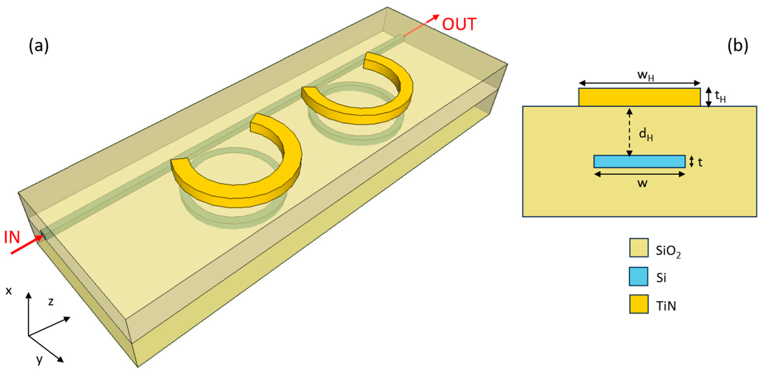
The key building block of the RF photonic filter is the optical notch filter. The proposed device comprises two cascaded silicon ring resonators (RRs), both having the same radius R. Each of these resonators can be individually thermally tuned, allowing for reconfigurability in both central frequency and bandwidth. The optical filter is sketched in
Figure 2.
The mathematical model used to characterize the filter response relies on the scattering matrix method [
21]. In particular, the scattering matrix of the whole system is calculated by the multiplication of the matrices related to the individual rings. Therefore, the transmission element (S
21 ≡ T
OUT) results as
where t
1 and t
2 are the S
21 elements of the scattering matrix of the RRs. They have been calculated also by using the scattering matrix theory, according to [
22]:
where k is the amplitude coupling coefficient,
is the amplitude transmission coefficient,
is the propagation constant, α is the propagation loss, and R is the ring radius, assumed as the same for both RRs. The effective refractive index (n
eff) has been calculated by using FEM simulations (COMSOL Multiphysics
® software Release 4.4), also taking into account the Sellmeier relationships and the presence of the TO phase shifters. The contribution of the TO phase shifters to the n
eff variation has been estimated through the combination of thermal and optical mode solvers and analyzing both the heat distribution and the efficiency. The presence of TiN TO phase shifters along the whole ring resonators’ optical path allows for the reconfigurability of both the central frequency and bandwidth. Further details are reported in
Section 3.2.
This configuration enables the complete overlap of the two spectral responses t1/2 when no current is applied to the electrodes, thereby enabling an extended tuning range.
The proposed filter is based on a silicon (Si) waveguide, fully embedded in silicon dioxide (SiO
2), that shows a width (w) of 440 nm and a thickness (t) of 220 nm, to ensure the single-mode operation. The modal analysis of the designed waveguide was made by using FEM simulations (COMSOL Multiphysics
® software), also taking into account the waveguide dispersion. Although lower values of propagation losses have been reported in the literature for the same waveguide [
23], we have considered a propagation loss value of α = 0.4 dB/cm at λ ≈ 1550 nm for the TE
0 mode [
24] to take into account additional losses associated with fabrication.
The design of both the radius R and the coupling coefficient k between the bus and both rings has been carried out, aimed at maximizing the stopband rejection. It has been observed that as the radius increases, the power coupling coefficient decreases, primarily due to the impact of the bending losses [
25]. To ensure decoupling between the two rings, they are spaced apart by a distance greater than 1 µm, where the coupling is negligible. The radius has been set to R = 10 µm to avoid increasing bending losses and obtain the desired central frequency (≈1550 nm). In the low-coupling regime of RRs, k = 2.24% ensures the BW − SBR trade-off. A gap g = 710 nm has been designed by performing the Beam Propagation Method (BPM) parametric simulations to obtain the desired coupling coefficient, guaranteeing a Lorentzian notch shape with an SBR of about 45 dB and a BW of 610 MHz. The impact of the variability in the fabrication process on the device’s performance has been also evaluated. In particular, by considering fabrication tolerances of ±10 nm on the gap, radius, and each waveguide width, an in-depth analysis has been carried out. To compare and properly understand each structure parameter’s effect on the operating wavelength, bandwidth, and stopband rejection, they have been modified one at a time. The combination of w = 430 nm, R = 10 μm − 10 nm, g = 700 nm and w = 450 nm, R = 10 μm + 10 nm, g = 720 nm for the first RR and the second RR, respectively, represents the worst case since the difference in BW and SBR between the two RRs is the highest. However, a bandwidth of 510 MHz and stopband rejection of 49 dB have been achieved; therefore, the device is robust to the fabrication tolerances.
3.1. Technological Platform
The proposed filter is supposed to be fabricated in SOI technology. This choice has been dictated by the fact that silicon photonics represents a transformative technology closely tied to the increasingly demanding performance requirements of the datacom and telecom sectors. This technology leverages well-established manufacturing infrastructure and mature platforms that are compatible with CMOS technology, allowing for its transition from research laboratories to industrial manufacturing facilities. Additionally, the high index contrast of silicon (=3.47 @ 1550 nm) compared to its surrounding materials (e.g., SiO2 with nSiO2 = 1.44 @ 1550 nm) ensures compactness, tight bend radii, high-density integration, and low power consumption due to its reduced size.
Thanks to advances in manufacturing techniques such as micro-transfer printing, hybrid integration, and wafer bonding, it is now possible to integrate high-bitrate germanium detectors, high-performance modulators, filters, routers, and even sources onto a single silicon chip [
26].
Indeed, silicon proves to be exceptionally well-suited for filters, primarily due to its ability to accommodate various tuning mechanisms. These mechanisms include the plasma dispersion effect achieved through carrier injection [
27], accumulation [
28] or depletion [
29], the Pockels effect when combined with piezo-materials [
30], the Franz–Keldysh effect when combined with germanium [
31], and the Quantum Confined Stark effect when it has been created with Ge-Si-Ge quantum wells [
32].
3.2. Tuning Mechanism
The reconfigurability of filters can be achieved by modifying the effective index n
eff of the guided mode. The two primaries are based on the thermo-optic effect [
33] and the electro-optic (EO) effect [
34].
The TO effect is exploited through a metal heater, fed by an electric current, and positioned close to the waveguide core. The heat generated as a result of the Joule effect in the metal induces a change in the refractive index of the waveguide, related to the Thermo-Optic Coefficient (TOC) of the material [
35]. Due to the remarkably high TOC of silicon (dn/dT = 1.80 × 10
−4 a.u. @ C band), the TO tuning method is well-suited for phase shifters. However, temperature change also affects the propagation losses (dα/dT = 4.39 × 10
−9 K
−1 @ C band). Two titanium nitride (TiN) electrodes with thickness t
H and width w
H have been positioned on top of RRs with a separation of d
H from the Si core (as depicted in
Figure 2b). Although ticker metal heaters ensure larger efficiency, fabrication constraints limit the thickness (t
H) to 100 nm [
36,
37]. Moreover, it is essential to avoid the deposition of the metal layer on the coupling region as thermal tuning can impact the coupling coefficient. Therefore, the electrodes are strategically positioned outside the coupling regions, and they show the same tuning lengths for all ring resonators (as illustrated in
Figure 2a). The overall electrode length of 25.12 µm has been chosen, ensuring the absence of electrodes within the coupling region, assumed as 20% of the total resonator length [
24].
The design of the gap between the metal layer and the waveguide (dH) is crucial to avoid absorption losses due to the metal, striking a balance between efficiency and losses. Small values of dH ensure good efficiency with large loss values.
Another crucial parameter for phase shifters is the response time (τ). This time is typically defined as the duration required to transition from 10% to 90% or from 90% to 10% of the final electrical input square pulse value, corresponding to the rising and falling times, respectively.
The design of all parameters has been conducted by integrating and harmonizing the capabilities of a thermal solver and an optical mode solver. This synergistic approach enabled the simulations to delve deeply into assessing various facets such as heat distribution, efficiency metrics, and the system’s transient response. A temperature of 300 K has been assumed as a boundary condition of the simulation domain. For the thermal simulations, heat capacities and thermal conductivities of 0.8 J/g°C and 150 W/mK, 0.8 J/g°C and 1.5 W/mK, and 0.5 J/g°C and 30 W/mK for silicon, silicon dioxide, and titanium nitride, respectively, have been considered. The design of d
H and w
H has been conducted, aimed at achieving low power consumption and minimizing the figure of merit (FOM), represented by FOM = P
π · τ, where P
π denotes the power necessary to achieve a phase shift of π. The reduction in w
H leads to a decrease in P
π, preserving the value τ [
36,
37]. Additionally, P
π can be reduced by increasing d
H, thereby enhancing heat insulation rather than conduction. However, the FOM decreases as w
H and d
H decrease. Therefore, w
H = 0.8 µm and d
H = 0.4 µm have been set with a resulting time response of τ = 9.20 µs and a P
π of 11.50 mW. These theoretical results align perfectly with experiments reported in the literature [
38].
4. Discussion
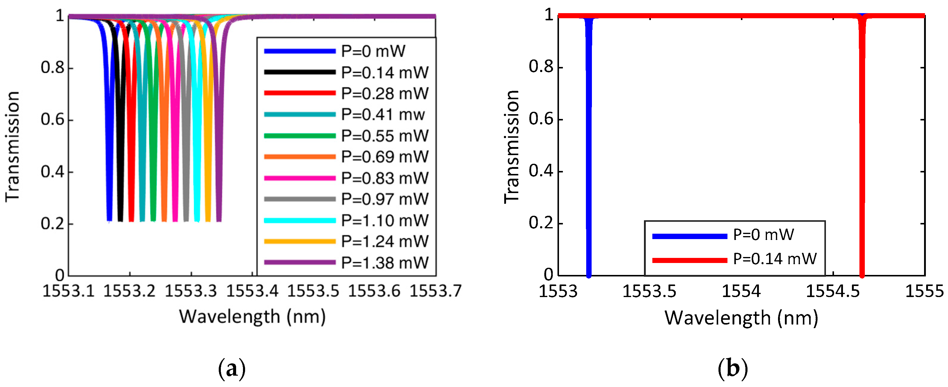
By tuning either one RR or both, the bandwidth or the central frequency can be tailored, respectively. When applying an electrical power ranging from 0 to 4.60 µW to the second RR, the bandwidth expands from about 500 MHz to 520 MHz, while maintaining the stopband rejection value (=45 dB). This broadening of the bandwidth is correlated to a red shift of the resonance peak of the second RR. As the two resonators cascade, this shift results in an overall enlargement of the filter envelope.
Another consequence is the slight shift of the central frequency, which varies by approximately 37 MHz (as shown in
Figure 3). Providing a higher current to the heater enables a broader bandwidth but also leads to an increase in in-band ripple, which compromises the desired filter flatness (as illustrated in the inset of
Figure 3).
If a shift in the central frequency is desired, both RRs need to be tuned. This configuration allows for adjustment of the central frequency of the notch filter without influencing the bandwidth. The Free Spectral Range (FSR) of both RRs is sufficiently wide to avoid resonance peak overlap when the feeding electrical power ranges from 0 to 11.50 mW. Therefore, this approach guarantees a central frequency shift spanning up to 180 MHz (as depicted in
Figure 4).
The maximum achievable shift is limited by the chosen tuning mechanism as higher power values can lead to more significant shifts but also higher losses. These losses lead to an increase in BW and a decrease in the SBR.
During the device operation, power values may deviate from their nominal ones. However, this does not strongly affect the overall performance. Indeed, as regards the bandwidth reconfigurability, the electrical power rounding up and down to the nearest integer yields a 5–10 MHz oscillation of the nominal bandwidth value. In the case of central wavelength tuning, the rounding up or down of the electric power poses no issue as the central frequency remains within the tuning range. Considering manufacturing tolerances of ±10 nm, the coupling coefficient could change within the range of ±1.4 × 10⁻³, consequently impacting both stopband rejection (34–72 dB) and the bandwidth (472–534 MHz) of the individual resonator.
The proposed filter successfully meets most of the requirements outlined in
Table 1, including in-band ripple (<0.5 dB), stopband rejection (45 dB), and power consumption (ranging from 0 to 11.50 mW). It accomplishes the target performance while maintaining a simple and compact architecture that aligns with the constraints of the
NewSpace Economy.
A further improvement of the FWHM could be achieved through the use of alternative technological platforms, such as silicon nitride (SiN) [
39], which shows losses 2 orders of magnitude lower than the SOI one. However, the main bottlenecks regard the thermo-optic efficiency of SiN, which results in one order of magnitude lower than the Si one, with a resulting smaller tuning range and/or larger power consumption.
The limited reconfigurability is associated with the chosen tuning mechanism, the thermo-optic effect, since higher power values can lead to more significant shifts but also higher losses, which strongly worsens the bandwidth and the stopband rejection. Concurrently, efforts are underway to explore techniques that can enhance the tuning range and reduce reconfiguration time, like the electro-optic effect [
34]. However, a fast reconfiguration time and low power consumption is achievable at the expense of a limited tunability range and a complex fabrication. One potential improvement lies in the use of nonvolatile materials. This innovative tuning mechanism seems to be promising in the development of switches, filters, lenses, absorbers, sensors, and more [
40,
41]. The goal is to meet all the requirements of a Tunable Bandpass Filter (BPF) and, thereby, create a fully flexible photonic telecommunication payload.
5. Conclusions
Reconfigurable photonic filters have garnered significant attention due to their potential to enhance the functionality of space payloads. These advanced devices harness the properties of propagating light to deliver superior performance in signal processing, filtering, and frequency selection.
In scenarios where satellite communication frequencies are congested, leading to multiple signals sharing the same spectrum, reconfigurable photonic filters simplify spectrum management and interference mitigation. This, in turn, ensures dependable signal transmission.
These advantages open doors to various applications in space payloads, including agile frequency channelization, enabling the simultaneous processing and analysis of diverse frequency bands. Through the adaptive suppression of unwanted interference, these filters enhance overall communication performance, simplifying signal processing algorithms. As a result, they improve both signal reception and transmission, allowing for precise and targeted communication with Earth stations and other space assets.
In this context, we have proposed a fully reconfigurable filter with an impressive stopband rejection of 45 dB. This filter comprises two tunable decoupled ring resonators capable of adjusting both bandwidth and central frequency. Achieving this tuning requires only a small amount of power (ranging from 0 to 11.50 mW), thanks to the efficient thermo-optic tuning of silicon. However, it is worth noting that this tuning process is relatively slow, taking 9.20 µs.
Our proposed filter can achieve, theoretically, a bandwidth reconfigurability of 20 MHz by heating one resonator. By feeding electric currents to both ring resonators, we can achieve a maximum central frequency shift of 180 MHz without affecting the bandwidth.


