Next Article in Journal
Antibacterial Activity of Endodontic Gutta-Percha—A Systematic Review
Previous Article in Journal
Assessing the Impact of Varied Dark Chocolate Concentrations on Enamel and Dentine Microhardness
Previous Article in Special Issue
Polarization Sensitivity in Scattering-Type Scanning Near-Field Optical Microscopy—Towards Nanoellipsometry
 
 
applsci-logo
Article Menu

Article Menu

Review

Quantum Information with Integrated Photonics

by
Paolo Piergentili
1,2,*,
Francesco Amanti
3,
Greta Andrini
4,5,
Fabrizio Armani
6,
Vittorio Bellani
7,8,
Vincenzo Bonaiuto
9,10,
Simone Cammarata
3,11,
Matteo Campostrini
12,
Samuele Cornia
8,13,
Thu Ha Dao
9,10,
Fabio De Matteis
9,10,
Valeria Demontis
8,14,
Giovanni Di Giuseppe
1,2,
Sviatoslav Ditalia Tchernij
5,15,
Simone Donati
3,16,
Andrea Fontana
8,
Jacopo Forneris
5,15,
Roberto Francini
9,10,
Luca Frontini
6,17,
Roberto Gunnella
1,2,
Simone Iadanza
18,
Ali Emre Kaplan
19,
Cosimo Lacava
8,20,
Valentino Liberali
6,17,
Francesco Marzioni
1,2,21,
Elena Nieto Hernández
5,15,
Elena Pedreschi
3,
Domenic Prete
8,
Paolo Prosposito
9,10,
Valentino Rigato
12,
Carlo Roncolato
12,
Francesco Rossella
8,13,
Andrea Salamon
10,
Matteo Salvato
10,22,
Fausto Sargeni
10,23,
Jafar Shojaii
24,
Franco Spinella
3,
Alberto Stabile
6,17,
Alessandra Toncelli
3,16,
Gabriella Trucco
6,25 and
Valerio Vitali
8,20
add Show full author list remove Hide full author list
1
Scuola di Scienze e Tecnologie, Divisione di Fisica, Università di Camerino, 62032 Camerino, Italy
2
Istituto Nazionale di Fisica Nucleare, Sezione di Perugia, 06123 Perugia, Italy
3
Istituto Nazionale di Fisica Nucleare, Sezione di Pisa, 56127 Pisa, Italy
4
Dipartimento di Elettronica e Telecomunicazioni, Politecnico di Torino, 10129 Torino, Italy
5
Istituto Nazionale di Fisica Nucleare, Sezione di Torino, 10125 Torino, Italy
6
Istituto Nazionale di Fisica Nucleare, Sezione di Milano, 20133 Milano, Italy
7
Dipartimento di Fisica, Università di Pavia, 27100 Pavia, Italy
8
Istituto Nazionale di Fisica Nucleare, Sezione di Pavia, 27100 Pavia, Italy
9
Dipartimento di Ingegneria Industriale, Università di Roma Tor Vergata, 00133 Roma, Italy
10
Istituto Nazionale di Fisica Nucleare, Sezione di Roma Tor Vergata, 00133 Roma, Italy
11
Dipartimento di Ingegneria dell’Informazione, Università di Pisa, 56122 Pisa, Italy
12
Laboratori Nazionali di Legnaro, Istituto Nazionale di Fisica Nucleare, 35020 Legnaro, Italy
13
Dipartimento di Scienze Fisiche, Informatiche e Matematiche, Università di Modena e Reggio Emilia, 41125 Modena, Italy
14
National Enterprise for nanoScience and nanoTechnology, Scuola Normale Superiore and Istituto Nanoscienze—Consiglio Nazionale delle Ricerche, 56127 Pisa, Italy
15
Dipartimento di Fisica, Università di Torino, 10125 Torino, Italy
16
Dipartimento di Fisica, Università di Pisa, 56127 Pisa, Italy
17
Dipartimento di Fisica, Università di Milano, 20133 Milano, Italy
18
Paul Scherrer Institute, 5232 Villigen, Switzerland
19
Optoelectronics Research Center, University of Southampton, Southampton SO17 1BJ, UK
20
Dipartimento di Ingegneria Industriale e dell’Informazione, Università di Pavia, 27100 Pavia, Italy
21
Dipartimento di Fisica, Università di Napoli “Federico II”, 80126 Napoli, Italy
22
Dipartimento di Fisica, Università di Roma Tor Vergata, 00133 Roma, Italy
23
Dipartimento di Ingegneria Elettronica, Università di Roma Tor Vergata, 00133 Roma, Italy
24
Space Technology and Industry Institute, Swinburne University of Technology, Hawthorn, VIC 3122, Australia
25
Dipartimento di Informatica, Università di Milano, 20133 Milano, Italy
*
Author to whom correspondence should be addressed.
Appl. Sci. 2024, 14(1), 387; https://doi.org/10.3390/app14010387
Submission received: 13 November 2023 / Revised: 28 December 2023 / Accepted: 28 December 2023 / Published: 31 December 2023
(This article belongs to the Special Issue Recent Advances and Future Trends in Nanophotonics Ⅱ)

Abstract

:
Since the 1980s, researchers have taken giant steps in understanding how to use quantum mechanics for solving real problems—for example, making a computer that works according to the laws of quantum mechanics. In recent decades, researchers have tried to develop a platform for quantum information and computation that can be integrated into digital and telecom technologies without the need of a cryogenic environment. The current status of research in the field of quantum integrated photonics will be reviewed. A review of the most common integrated photonic platforms will be given, together with the main achievements and results in the last decade.

1. Introduction

The idea of building a computer based on the manipulation of quantum systems dates back to the early 1980s, when R. P. Feynman, among others, proposed in his pioneering work [1] to build a computer based on the principles of quantum mechanics, to simulate nature. In 1984, Bennett and Brassard proposed the first quantum key distribution (QKD) algorithm [2] based on the principles of quantum mechanics for the amplification and distribution of secure cryptographic keys. In 1992, Bennett together with Wiesner proposed the dense coding protocol that in quantum communication allows the transfer of a number of classical bits of information, using a smaller number of qubits [3]. In 1993, the protocol of quantum teleportation was proposed, to overcome the distance limitations in transferring a quantum state [4]. In the following decades, many quantum algorithms able to outperform the corresponding classical ones were developed, such as Grover’s quantum-search algorithm [5] and Shor’s factoring algorithm [6]. At the end of the last century, Schumacher established the analogy to Shannon’s theorems, and the beginning of the new millennium saw the formal definition by DiVincenzo of the physical requirements for the practical implementation of a universal quantum computer [7]: (i) ability to initialize the state of the qubits; (ii) ability to implement a universal quantum gate; (iii) coherence time larger than the gate operation time; (iv) qubit measurement capability; (v) scalability. Since then, several technologies have been proposed for practical usage based, e.g., on superconducting [8], trapped ions [9], photonic [10] and silicon technologies [11]. Several realizations of qubits and implementations of quantum gates have been conceived. The simplest, but universal, prototype of this kind of circuit is the two-qubit controlled–NOT-(CNOT) gate. It operates by flipping the state of a target qubit in the computational basis | 0 T , | 1 T only if the control qubit is in the state | 1 C (see Box 1).
The challenge, which is currently being addressed, remains the establishment of a scalable and convenient platform for practical implementation of quantum technologies. Such quantum technologies include protocols and devices able to perform computations that are much more time-efficient than their classical counterparts. In recent years, IBM [12] and Google [13] have realized prototypes of commercial quantum computers. They use superconducting qubits by means of the superposition of supercurrents in Josephson junctions, which require very low temperatures to operate. Also, superconducting opto-electronic circuits integrated with photonic components have been explored for fast, energy-efficient computation [14], photon detection [15,16], and transduction between microwaves and optical photons [17,18]. However, these new quantum technologies should be simply integrable into the systems and infrastructures that have been developed for digital and telecom information technologies. This requirement has oriented researchers towards the development of integrated photonics chips in silicon [11,19,20,21]. Due to their potential integration into and compatibility with the complementary metal–oxide-semiconductor-(CMOS) fabrication process at the heart of the digital era, silicon-based-integrated-photonics architectures are promising candidates for integrated-quantum-photonics devices, which do not require an ultra-cryogenic environment. In this view, integrated quantum photonics provides a versatile platform for on-chip generation, processing, and detection of quantum states of light [6,7]. The aim is the development and implementation of a complete silicon-photonics integrated circuit for quantum computation. However, the lack of photon–photon interaction without a non-linear matter mediator makes such a proposal challenging. In 2001, a breakthrough was achieved with the introduction by Knill, Laflamme, and Milbourn [22] of probabilistic-gate-based quantum computation by means of linear optics (the KLM scheme). On this basis, they demonstrated that the missing photon–photon interaction required for realizing quantum gates can be implemented by suitable conditioning through photodetection represented by measurement-induced nonlinearity [11,22,23]. The price to pay is the lack of determinacy: linear-optics quantum computation (LOQC) is inherently non–deterministic that is, the successful results of the computation are a distinguishable post-selected subset of all possible outputs, although the scalability was demonstrated. Recently, companies have been founded for providing a quantum-photonics approach to problem solving [24,25,26].
Applsci 14 00387 i001
In this review, we explore the current status of research in the field of quantum integrated photonics, and we describe the main achievements and results in the field of integrated-linear-optics quantum computation that were not contained in the previous reviews [20,21].

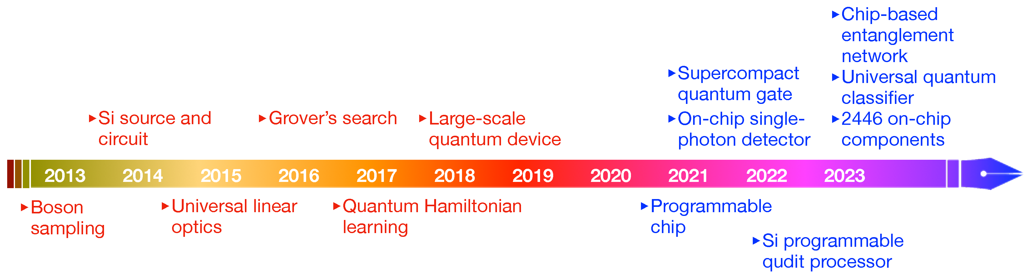
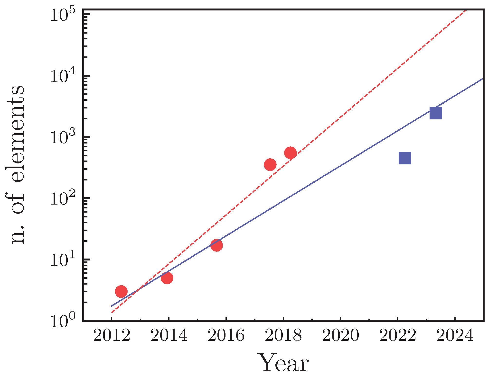
2. The Beginning of Integrated Quantum Photonics

The main element of LOQC is the beam splitter (the directional coupler in waveguide terminology) with an arbitrary reflection coefficient, which superimposes the state of light, properly guided (see Box 1). The paths the photons might take are the degrees of freedom for encoding qubits. O’Brien et al. [27] provided the first experimental verification of KLM gates by means of bulk optics. However, for scalability and miniaturization, the use of waveguides and directional couplers is preferred. Two approaches have been followed for this scope. One consists in focusing an intense laser on a doped silica layer or on a glass substrate, allowing the creation of arbitrary waveguide structures [28]. The other method, described for the first time in 2008 by Politi et al. [29], is represented by silica-on-silicon-waveguides quantum circuits, where high-fidelity integrated implementations of key components of photonic quantum circuits are demonstrated. In their paper, the fabrication of several directional couplers with different splitting ratios was reported, in order to prove the reproducibility of such devices, which are the main building element of the integrated CNOT gate. The waveguides were made of a silica core doped with germanium and boron oxides. Degenerate photon pairs at 804 n m were generated outside and injected into the chips. They also fabricated the first integrated CNOT gate, and experimentally tested its functionality by using only the four states of the computational basis ( | 0 C | 0 T , | 0 C | 1 T , | 1 C | 0 T , and | 1 C | 1 T ) and measuring the probability of detecting each of the computational states at the output. The average fidelity for the logical basis was ( 94.3 ± 0.2 )%. For the first time, a single chip had the ability to implement all the elements necessary to realize an on-chip LOQC-based CNOT gate. However, by using only the states of the computational basis, it was not possible to demonstrate the entanglement/disentanglement property of the CNOT. Those limits were exceeded by including on-chip waveguide interferometers with variable phase shifters to precisely control the state of the qubits and to realize the entanglement of multi-photons directly on chip [30]. In the same year, the first Shor’s factoring algorithm proof of principle using a SiO2 chip with two CNOT gates was demonstrated [31], implementing a compiled version of Shor’s algorithm for factorizing 15.
With such preliminaries, in 2012, Shadbolt et al. [32] realized an integrated-quantum-photonic device comprising a two-qubit entangling gate, eight variable phase shifters, and many Hadamard-like gates. This device was able to characterize both arbitrary single-photon states with any amount of mixture and pure two-photon states with any amount of entanglement. High fidelity for thousands of randomly chosen configurations was achieved. However, the photon sources used for such tests were still bulk devices out of the chip. The first advancement (see Figure 1) towards a fully integrated chip for quantum circuit applications was achieved in 2013 [33]. A bright pump laser, coupled to the chip using a lens fiber and on-chip spot-size converters, and distributed between two spiraled waveguides, excited the χ ( 3 ) spontaneous four-wave mixing effect, to produce signal–idler photon pairs. The pairs generated in the two spiraled waveguides interfered on a coupler, to yield either splitting or bunching over the two output modes, depending on the phase, which was thermo-optically reconfigurable. This allowed, for the first time, an on-chip source of photons, although detection was still made outside the chip. The chip was realized on a silicon-on-insulator (SOI) photonic platform, to have full compatibility at telecom wavelength, and quantum interference up to ( 100 ± 0.4 )% was achieved. The pairs generated from the device were also tested and used for off-chip Hong–Ou–Mandel experiments, obtaining visibility up to ( 95 ± 4 )%.

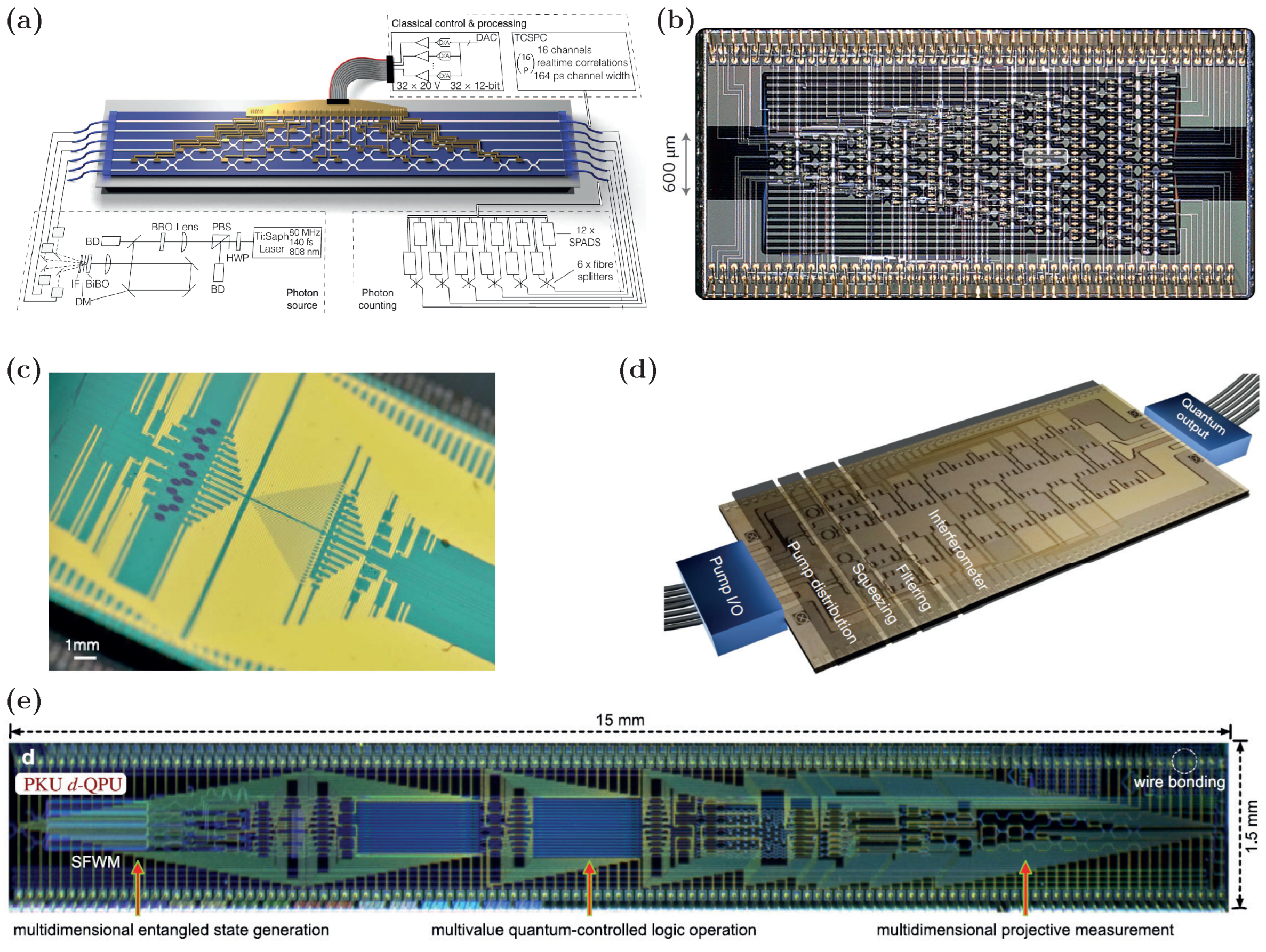
3. Integrated Quantum Photonics Systems

To enhance the quantum information and computation integrability and scalability, researchers have dealt with the problem of increasing the circuit complexity.
Photonic Processors—Since 2017, improved technologies and fabrication processes have allowed the realization of much more complex integrated circuits able to perform many operations on the chip. A SOI-quantum-photonic device that integrates the capabilities for the generation, manipulation, and analysis of two-qubit entangled states has been reported [49]. The device can prepare and operate on a variety of separable and entangled states, using a switchable entangling gate. The performances were measured using on-chip quantum-state tomography.
The increasing number of elements in a single device brought about the birth of the first quantum photonic processor, which consisted of a programmable single device able to perform many different operations. One of the first reconfigurable integrated quantum photonic processors was developed in 2015 by Carolan et al. [39]. Such a universal linear-optic processor heralded both quantum logic gates and entangling gates, by means of 15 Mach–Zehnder interferometers made of 30 silica-on-silicon-waveguides directional couplers and 30 electronically controlled phase-shifters, programmed with four micro-controllers with a total 32-channel 12–bit digital-to-analogue converters. A picture of the photonic processor is shown in Figure 2a. The processor was also programmed to implement 100 different boson-sampling routines. Boson sampling, which is believed to require exponential time by using classical resources, is a computational task that samples from the output of a linear-network interferometer the distribution of identical photons sent into it [50,51].
Silicon chips started to integrate more and more elements and, in 2017, Harris et al. [52] realized a programmable nanophotonic chip made up of 264 elements [see Figure 2b]: 88 interferometers and 176 individually tunable phase shifters, which could be programmed by means of a 240–channel, 16–bit precision electronic biasing system. The authors, using such a processor, simulated different transport regimes over a set of 64,400 experiments, observing also the signatures of the environment-assisted quantum transport: a particle propagating through a strong disordered system became exponentially localized in space (Anderson localization), inhibiting transport; still, increasing environmental noise over a finite range resulted in enhanced transport.
Later on, in 2018, more than 200 photonic components were used to realize a fully programmable quantum circuit with two qubits [53]. CMOS-compatible processing was used for fabrication. The quantum processor was programmed to compute 98 different quantum operations with two qubits, with an average quantum-process fidelity of ( 93.2 ± 4.5 )%. On the same track, Wang et al. [42] realized an integrated multidimensional quantum photonic platform that had more than 550 photonic components [see Figure 2c]. It implemented the generation, manipulation, and analysis of multi-dimension quantum systems directly on a single chip.
In 2021, Arrazola et al. [43] realized a programmable nanophotonic chip. A rendering of the photonic processor is presented in Figure 2d. Four micro-ring resonators generated two-mode squeezed states, achieving large-photon-number event rates: with the four squeezers activated, the 4-photon detection rate reached, on average, 10,000 events per second, and the 19-photon an average rate of 0.3 events per second. An external computer ran custom-developed control software to operate the chip, which was programmable by means of a classical computer and python libraries, allowing dummy users to run remotely quantum algorithms directly on the device. To prove the quantum advantage of using this photonic hardware, the authors performed the boson-sampling algorithm, which was mapped to the calculation of molecular spectra. The chip was used for a proof-of-principle demonstration of the evaluation of the Franck–Condon spectra of ethylene and (E)–phenylvinylacetylene, without the need to evaluate the usual Franck–Condon factors, which represented a computational hard task [54].
A photonic quantum chip with 95 phase shifters and 355 optical components was realized by Chen et al. [55]. This chip represented a platform on which to study the quantum superposition of coherent multimode states—in particular, a generalized multipath wave–particle duality. The transition between the full-particle nature and full-wave nature was obtained for a classical mixture and a quantum superposition. One year later, the same group presented an advanced chip a quantum processing unit [45], that integrated all the necessary components to initialize, manipulate, and measure quantum-quart (ququart) states. It was composed of 451 photonic components, including 116 reconfigurable phase shifters, which could be directly addressed and controlled by using the co-integration technology of photonic and electronic circuits in silicon [see Figure 2e]. The authors proved that quantum computation based on a qudit of dimension d, together with integrated photonics, can increase quantum parallelism with reference to computational accuracy, capacity, and efficiency, compared to its counterpart of quantum computing based on qubits. Specifically, the computational capacity of a four-qubit processor can be equivalently achieved by a two-ququart quantum processor. Encoding each qudit in a dimension d, keeping the same number of photons, improves the detection rate of photons. Furthermore, computational efficiency and speed-up are enhanced by multiple-path interference.
One of the most complicated quantum-photonics devices, in terms of circuitry complexity and functionality, was realized in 2023 by Zheng et al. [46]. A multi-chip multidimensional quantum-entanglement network with retrievability was demonstrated by using silicon–photonic-hybrid-multiplexing technologies. The full spectrum of hybrid encoding and multiplexing devices was monolithically integrated on chips. Moreover, the scalability of integrated quantum devices, networking architecture, multi-mode fiber channels, and entanglement retrieving techniques was demonstrated and verified. Three pairs of three-dimensional entangled photons were distributed from the server chip to three node chips through three few-mode fibers. Then, a quantum-entanglement-retrieving algorithm was used to retrieve entanglement, and quantum tomography was performed. An average fidelity of 89.0% was obtained.
A 12-mode programmable photonic chip implementing arbitrary linear-optical transformations on 12 waveguides was used to simulate the unitary evolution of a global isolated system and to demonstrate that the initial state of a local subsystem evolves towards a state of maximum entropy—that is, to a thermal ensemble, due to entanglement with the other modes of the global system [56].
Boson sampling—Photonics systems have also been studied to achieve boson sampling, which is a good candidate for quantum supremacy. Since 2013, Spagnolo et al. [57] reported on the first experimental observation of three-photon interference in an integrated three-port directional coupler (tritter) realized by ultrafast-laser-writing waveguides in a borosilicate-glass substrate. The tritter made three photons interact simultaneously without having to decompose the process into cascaded two-mode interactions and phase shifters. In Ref. [38], a quantum-boson-sampling machine with a silica-on-silicon waveguide was reported. The integrated photonic circuit sampled the output distribution resulting from the nonclassical interference of three and four photons. A larger photonic chip for boson-sampling experiments was realized and reported in Ref. [58]. The authors reported on photonic-boson-sampling experiments in randomly designed integrated chips with 5, 7, 9, and 13 modes, which corresponded to 10, 35, 84, and 286 different no-collisions outputs. The waveguides were directly fabricated in the glass chip. In 2022, Madsen et al. [59] realized a programmable photonic processor, named Borealis, showing a quantum-computational advantage by carrying out Gaussian boson sampling on 216 squeezed entangled modes. By using the best classical resources available, it would take more than 9000 years, on average, to get a single sample output, whereas Borealis required only 36 μ s . Among all the photonic demonstrations of quantum computational advantage, photonic or otherwise, Borealis uses the largest number of independent quantum systems. Recently, Ono et al. experimentally realized a universal bosonic quantum classifier of classical data [47]. Quantum classification has three main steps: encoding data into a quantum state, processing the state, and measuring. Then, a classification model is built, with the parameters characterizing the classifier. A bosonic system consisting of a three-layer two-mode circuit and a two-photon input state was fabricated. By training a part of the circuit, it was possible to classify points inside an elliptical boundary, with a success probability of ( 94 ± 0.8 )%. Boson sampling, by its very nature, is a quantum algorithm, whose solution might not be efficiently verifiable. Indeed, any experimental instance approaching the regime of quantum advantage must be necessarily accompanied by appropriate evidence that the employed device is correctly performing the sampling process [20,60].
Quantum Key Distribution—Nowadays, security in exchanging encrypted messages is a crucial issue. QKD is a corroborated approach to generating a secret key at a distance in a secure way, because QKD relies on quantum mechanics laws and not on computational complexity. A fundamental step, in order to industrialize QKD systems, is miniaturization, with advantages in terms of mass production, low cost, simple stabilization in temperature, scalability, and compatibility with CMOS production. Sax et al. [61] realized an integrated QKD system at 2.5   G Hz , which featured a polarization-independent receiver and precise state preparation. At a distance of 151.5   k m of standard single-mode fiber, a secure key rate of 1.3   k / s was obtained, as well as a very low quantum-bit error rate, 0.9 %, at a distance of 202 k m . The device consisted of an integrated silicon photonics chip, comprising a photonic integrated circuit of dimension 4.50 × 1.10   m m 2 with an adjacent electronic-driver integrated circuit of 4.50 × 0.75   m m 2 . The integrated circuits were then bounded and integrated into a small printed circuit board combined with a second, larger printed circuit board connected to all the electrical signals needed and to a computer-controlled FPGA (field-programmable gate array).

4. New Challenges for Quantum Photonics

Miniaturization—With the progress of chip complexity, researchers have had to face the unavoidable problem of miniaturization, which represents a significant challenge for quantum technologies. Zhang et al. [44] implemented a CNOT gate with a footprint of 4.8 × 4.45   μ m 2 that corresponded to about ∼ 3 λ × 3 λ . The chip was realized with standard fabrication processes, and it was fully compatible with SOI waveguides. They used silicon-superlattice waveguides, and by choosing different core widths of the waveguides (the symmetry-breaking strategy) they could arrange very dense uncoupled waveguides. To prove the functionality of the chip, the authors measured the truth table of the CNOT gate, demonstrated the generation of the four Bell states, and performed quantum-process tomography with a fidelity result of ( 92.5 ± 0.8 )%.
Optical elements—With the increase in integrated quantum photonics devices, researchers have been developing more efficient optical elements. For example, in 2021, Tasker et al. [62] interfaced CMOS silicon and germanium-on-silicon nanophotonics with integrated electronics, to realize a balanced homodyne detector with a bandwidth of 1.7   G Hz and shot noise limited up to 9 M Hz . All the linear optics needed to realize the homodyne detector, useful for measuring squeezed states, were integrated on the chip [see Figure 3a]. To test the performance of the device, a continuous spectrum of squeezed light was measured from 100 M Hz to 9 G Hz , and homodyne tomography was performed, to prove the ability of the chip to reconstruct quantum states. In 2023, Yu et al. [63] realized an on-chip electro-optic optical isolator with an achieved optical isolation of 48 dB. The optical isolator was tunable in wavelength from 1510 nm to 1630 nm, keeping an isolation larger than 37 dB. This element will help the integration of laser sources in photonics.
Encoding—Another approach to optimizing and increasing quantum resources is to exploit more available degrees of freedom. In this regard, in 2022, Feng et al. [64] realized the first multimode implementation of a 2-qubit quantum gate. They built a very compact CNOT gate with waveguides able to support two orthogonal transverse modes, in which the qubits were encoded. To prove the functionality of the device, two separate qubits were entangled, with an average fidelity of ( 89 ± 2 )%. The idea, to enlarge the dimension of the suitable Hilbert space by means of further degrees of freedom, was also exploited by Cheng et al. in Ref. [65], who realized a SWAP gate by encoding the information in the two degrees of freedom: polarization and spatial momentum. The SWAP gate was engineered, concatenating three CNOT gates. An average fidelity of ( 97.3 ± 0.3 )% of the output spatial-momentum states validated the single-qubit conversion from polarization qubit to spatial-momentum qubit. A process fidelity of ( 94.9 ± 1.0 )% was achieved for the on-chip two-qubit SWAP operation, with a process purity of ( 93.3 ± 1.0 )%.
Swapping between path and polarization degrees of freedom was also used for the first quantum photonic interconnection [66]. High-fidelity entanglement manipulation and distribution between two separate photonic chips was realized. Using on each chip a two-dimensional grating coupler, entangled states encoded in the path degree of freedom and generated on the chip were delivered to another chip by interconverting between polarization and path degrees of freedom.
Protocols—The possibilities offered by the new devices have opened the way to reconsidering schemes and protocols able to claim quantum supremacy. In this regard, graphs are discrete mathematical tools able to model quantum-mechanical devices and systems. An integrated graph-based quantum device, consisting of a synthetic two-dimensional 4 × 4 lattice, fully programmable, and made of reconfigurable linear-optical waveguide circuits and switchable nonlinear photon-pair sources, has been realized [48] [see Figure 3b]. The photon pair was generated using a nonlinear waveguide. It integrated 2446 components in total. The device could be schematized as eight vertex graphs: each path from one source to one detector of single photons represented a vertex, and each photon-pair source connecting two separate pathways represented an edge. The authors reconfigured the device to generate genuine multiphoton multidimensional entanglement, to manipulate and finally certify it.
Chen et al. realized a silicon photonic chip to generate and control four-photon Dicke states [67]. The indistinguishability of the photon pair emitted by the sources was characterized via a reverse Hong–Ou–Mandel experiment. High visibility for the | Ψ + and the | Φ Bell’s states was measured, showing the high quality of spectral overlap and qubit entanglement. Moreover, it demonstrated the coherent control of two-photon Bell states. Then, four-photon Dicke states were generated, and quantum-state tomography was performed, obtaining average fidelity of ( 82.3 ± 0.3 )%. These results show the high quality of the multiphoton sources. A signal enhancement of 7 dB was demonstrated by means of the inverse-weak-value amplification technique. It consisted of measuring the phase shift, with the signal amplified by the known spatial-phase front tilt. As the background noise was not increased, a 7 dB signal-to-noise ratio improvement was also shown. The Mach–Zehnder interferometer is built on-chip on a CMOS photonic platform, and all the elements of the chip are individually characterized. Weak-value amplification is embedded into measurement schemes that make use of linear-optics unitary transformations. Therefore, weak-value amplification does not have any advantage when the measurement is limited by the quantum nature of light—for example, the presence of shot noise, in the case of coherent beams. However, many times the information of the quantum state is covered by technical noises. In these cases, weak-value amplification allows, in principle, for distinguishing the states with a lower probability of error [68].

5. Conclusions and Outlook

The photonics community has taken extraordinary steps towards the milestone of realizing an on-chip quantum microprocessor. We have highlighted the main results in this area and have indicated the new challenges for developing a standalone quantum computer based on integrated photonics. The number of components doubles approximately every year [see Figure 4], which appears to be twice the Moore’s law for electronic integrated circuits [69]. The dependence and performance of computational tasks on the dimension of space and circuit elements was analyzed in Ref. [70]. Other open challenges for the achievements of the milestone have not been discussed: the realization of sources and detectors on chip for a standalone integrated photonic quantum device, and the coupling and control of the degrees of freedom of guided light by using nanomaterials. Indeed, much effort is still needed to fully integrate in only one chip photonic processors with sources and detectors. A photon source interfaced with a programmable integrated circuit has been recently achieved [71]. The compatibility of the CMOS fabrication processes will boost the fabrication of much larger programmable photonic processors with more qubits, able to implement more complex algorithms. Although improvements in the fabrication processes have brought to the achievement of quantum interference near-unity visibility and qubit operation with extremely low error [33,52], fabrication errors and variability may arise when the production is extended to full-silicon-wafer scale. These might be mitigated by the demonstrated high programmability of the recent photonic processors assisted by classical algorithms.

Author Contributions

All authors contributed to this work: writing—original draft preparation, P.P. (Paolo Piergentili) and G.D.G.; writing—review and editing, all authors. All authors have read and agreed to the published version of the manuscript.

Funding

This work was funded by INFN through the CSN5 QUANTEP project.

Acknowledgments

V.B. (Vittorio Bellani), G.D.G., A.F., R.G., C.L., E.P., P.P. (Paolo Piergentili), V.R., C.R., A.S. (Andrea Salamon), and F.S. (Franco Spinella) acknowledge the support of the PNRR MUR project PE0000023-NQSTI (Italy).

Conflicts of Interest

The authors declare no conflicts of interest.

Abbreviations

The following abbreviations are used in this manuscript:
CMOScomplementary metal–oxide semiconductor
CNOTcontrolled NOT
FPGAfield-programmable gate array
KLMKnill–Laflamme–Milburn
LOQClinear-optics quantum computation
MMImultimode interferometer
QKDquantum key distribution
SOIsilicon-on-insulator

References

  1. Feynman, R.P. Simulating physics with computers. Int. J. Theor. Phys. 1982, 21, 467–488. [Google Scholar] [CrossRef]
  2. Bennett, C.H.; Brassard, G. Quantum cryptography: Public key distribution and coin tossing. In Proceedings of the IEEE International Conference on Computers, Systems and Signal Processing, Bangalore, India, 10–12 December 1984. [Google Scholar]
  3. Bennett, C.H.; Wiesner, S.J. Communication via One- and Two-Particle Operators on Einstein-Podolsky-Rosen States. Phys. Rev. Lett. 1992, 69, 2881–2884. [Google Scholar] [CrossRef] [PubMed]
  4. Bennett, C.H.; Brassard, G.; Crépeau, C.; Jozsa, R.; Peres, A.; Wootters, W.K. Teleporting an Unknown Quantum State via Dual Classical and Einstein-Podolsky-Rosen Channels. Phys. Rev. Lett. 1993, 70, 1895–1899. [Google Scholar] [CrossRef] [PubMed]
  5. Grover Lov, K. A fast quantum mechanical algorithm for database search. In Proceedings of the Twenty-Eighth Annual ACM Symposium on Theory of Computing. STOC ’96, Philadelphia, PA, USA, 22–24 May 1996; pp. 212–219. [Google Scholar]
  6. Shor, P.W. Polynomial-Time Algorithms for Prime Factorization and Discrete Logarithms on a Quantum Computer. SIAM J. Comput. 1997, 26, 1484–1509. [Google Scholar] [CrossRef]
  7. DiVincenzo, D.P. The Physical Implementation of Quantum Computation. Fortschritte Der Phys. 2000, 48, 771–783. [Google Scholar] [CrossRef]
  8. Nakamura, Y.; Pashkin Yu., A.; Tsai J., S. Coherent control of macroscopic quantum states in a single-Cooper-pair box. Nature 1999, 398, 786–788. [Google Scholar] [CrossRef]
  9. Wineland, D.J.; Monroe, C.; Itano, W.M.; Leibfried, D.; King, B.E.; Meekhof, D.M. Experimental Issues in Coherent Quantum-State Manipulation of Trapped Atomic Ions. J. Res. Natl. Inst. Stand. Technol. 1998, 103, 259–328. [Google Scholar] [CrossRef]
  10. Braunstein, S.L.; van Loock, P. Quantum information with continuous variables. Rev. Mod. Phys. 2005, 77, 513–577. [Google Scholar] [CrossRef]
  11. O’Brien, J.L.; Furusawa, A.; Vučković, J. Photonic Quantum Technologies. Nat. Photonics 2009, 3, 687–695. [Google Scholar] [CrossRef]
  12. Kim, Y.; Eddins, A.; Anand, S.; Wei, K.X.; Van Den Berg, E.; Rosenblatt, S.; Nayfeh, H.; Wu, Y.; Zaletel, M.; Temme, K.; et al. Evidence for the Utility of Quantum Computing before Fault Tolerance. Nature 2023, 618, 500–505. [Google Scholar] [CrossRef]
  13. Arute, F.; Arya, K.; Babbush, R.; Bacon, D.; Bardin, J.C.; Barends, R.; Biswas, R.; Boixo, S.; Brandao, F.G.; Buell, D.A.; et al. Quantum supremacy using a programmable superconducting processor. Nature 2019, 574, 505–510. [Google Scholar] [CrossRef] [PubMed]
  14. Khan, S.; Primavera, B.A.; Chiles, J.; McCaughan, A.N.; Buckley, S.M.; Tait, A.N.; Lita, A.; Biesecker, J.; Fox, A.; Olaya, D.; et al. Superconducting Optoelectronic Single-Photon Synapses. Nat. Electron. 2022, 5, 650–659. [Google Scholar] [CrossRef]
  15. Schuck, C.; Guo, X.; Fan, L.; Ma, X.; Poot, M.; Tang, H.X. Quantum Interference in Heterogeneous Superconducting-Photonic Circuits on a Silicon Chip. Nat. Commun. 2016, 7, 10352. [Google Scholar] [CrossRef] [PubMed]
  16. Gyger, S.; Zichi, J.; Schweickert, L.; Elshaari, A.W.; Steinhauer, S.; Covre Da Silva, S.F.; Rastelli, A.; Zwiller, V.; Jöns, K.D.; Errando-Herranz, C. Reconfigurable Photonics with On-Chip Single-Photon Detectors. Nat. Commun. 2021, 12, 1408. [Google Scholar] [CrossRef] [PubMed]
  17. Youssefi, A.; Shomroni, I.; Joshi, Y.J.; Bernier, N.R.; Lukashchuk, A.; Uhrich, P.; Qiu, L.; Kippenberg, T.J. A Cryogenic Electro-Optic Interconnect for Superconducting Devices. Nat. Electron. 2021, 4, 326–332. [Google Scholar] [CrossRef]
  18. Lecocq, F.; Quinlan, F.; Cicak, K.; Aumentado, J.; Diddams, S.A.; Teufel, J.D. Control and Readout of a Superconducting Qubit Using a Photonic Link. Nature 2021, 591, 575–579. [Google Scholar] [CrossRef]
  19. Flamini, F.; Spagnolo, N.; Sciarrino, F. Photonic Quantum Information Processing: A Review. Rep. Prog. Phys. 2019, 82, 016001. [Google Scholar] [CrossRef]
  20. Wang, J.; Sciarrino, F.; Laing, A.; Thompson, M.G. Integrated Photonic Quantum Technologies. Nat. Photonics 2020, 14, 273–284. [Google Scholar] [CrossRef]
  21. Elshaari, A.W.; Pernice, W.; Srinivasan, K.; Benson, O.; Zwiller, V. Hybrid Integrated Quantum Photonic Circuits. Nat. Photonics 2020, 2020 14, 285–298. [Google Scholar] [CrossRef]
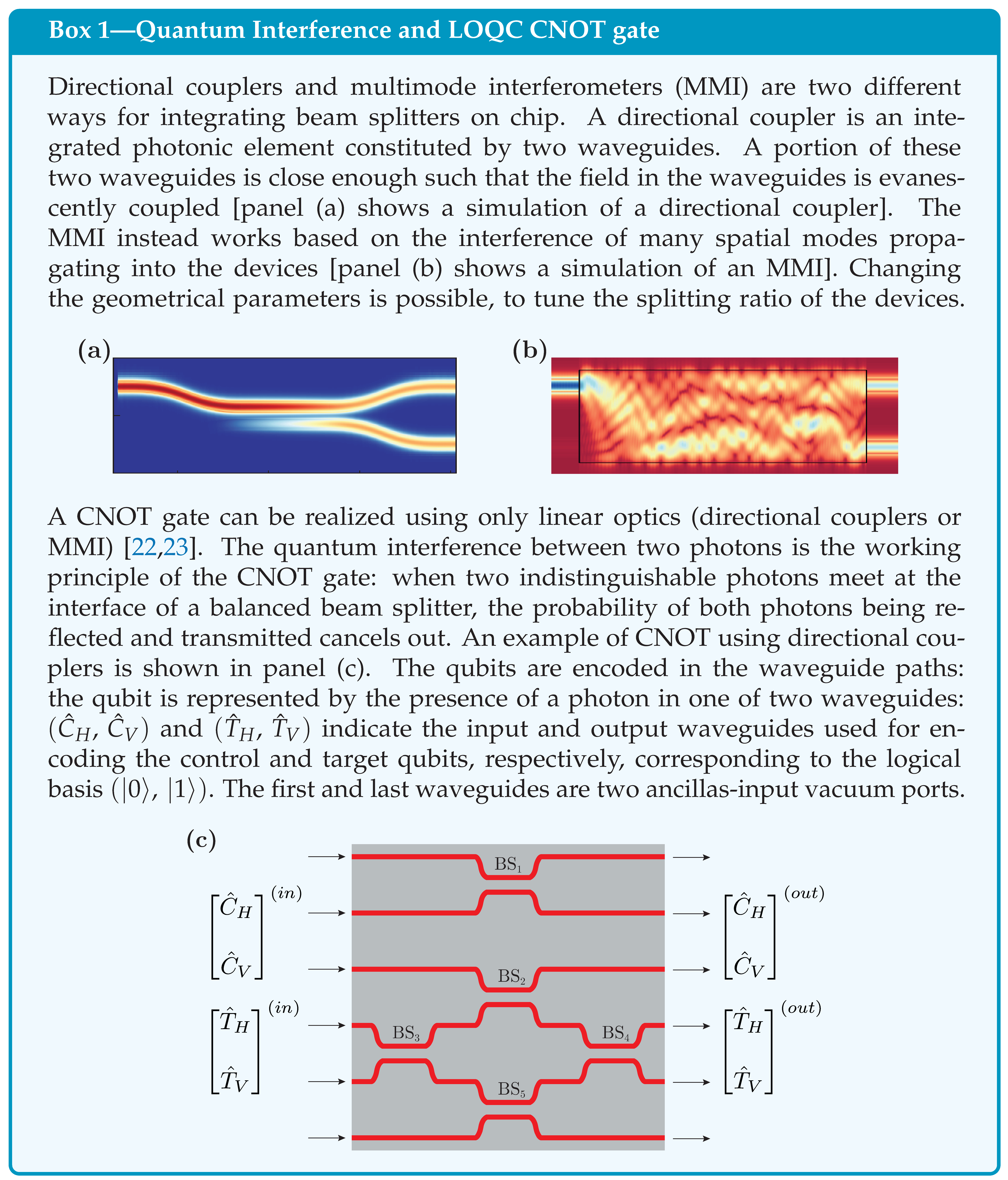
  22. Knill, E.; Laflamme, R.; Milburn G., J. A Scheme for Efficient Quantum Computation with Linear Optics. Nature 2001, 409, 46–52. [Google Scholar] [CrossRef]
  23. Ralph, T.C.; Langford, N.K.; Bell, T.B.; White, A.G. Linear optical controlled—NOT gate in the coincidence basis. Phys. Rev. A 2002, 65, 062324. [Google Scholar] [CrossRef]
  24. Available online: https://www.quandela.com/ (accessed on 8 August 2023).
  25. Available online: https://www.quixquantum.com/ (accessed on 8 August 2023).
  26. Available online: https://www.psiquantum.com/ (accessed on 8 August 2023).
  27. O’Brien, J.L.; Pryde, G.J.; White, A.G.; Ralph, T.C.; Branning, D. Demonstration of an All-Optical Quantum Controlled-NOT Gate. Nature 2003, 426, 264–267. [Google Scholar] [CrossRef] [PubMed]
  28. Crespi, A.; Osellame, R.; Ramponi, R.; Bentivegna, M.; Flamini, F.; Spagnolo, N.; Viggianiello, N.; Innocenti, L.; Mataloni, P.; Sciarrino, F. Suppression Law of Quantum States in a 3D Photonic Fast Fourier Transform Chip. Nat. Commun. 2016, 7, 10469. [Google Scholar] [CrossRef] [PubMed]
  29. Politi, A.; Cryan, M.J.; Rarity, J.G.; Yu, S.; O’Brien, J.L. Silica-on-Silicon Waveguide Quantum Circuits. Science 2008, 320, 646–649. [Google Scholar] [CrossRef] [PubMed]
  30. Matthews, J.C.F.; Politi, A.; Stefanov, A.; O’Brien, J.L. Manipulation of Multiphoton Entanglement in Waveguide Quantum Circuits. Nat. Photonics 2009, 3, 346–350. [Google Scholar] [CrossRef]
  31. Politi, A.; Matthews, J.C.F.; O’Brien, J.L. Shor’s Quantum Factoring Algorithm on a Photonic Chip. Science 2009, 325, 1221. [Google Scholar] [CrossRef] [PubMed]
  32. Shadbolt, P.J.; Verde, M.R.; Peruzzo, A.; Politi, A.; Laing, A.; Lobino, M.; Matthews, J.C.F.; Thompson, M.G.; O’Brien, J.L. Generating, Manipulating and Measuring Entanglement and Mixture with a Reconfigurable Photonic Circuit. Nat. Photonics 2012, 6, 45–49. [Google Scholar] [CrossRef]
  33. Silverstone, J.W.; Bonneau, D.; Ohira, K.; Suzuki, N.; Yoshida, H.; Iizuka, N.; Ezaki, M.; Natarajan, C.M.; Tanner, M.G.; Hadfield, R.H.; et al. On-Chip Quantum Interference between Silicon Photon-Pair Sources. Nat. Photonics 2014, 8, 104–108. [Google Scholar] [CrossRef]
  34. Crespi, A.; Osellame, R.; Ramponi, R.; Brod, D.J.; Galvão, E.F.; Spagnolo, N.; Vitelli, C.; Maiorino, E.; Mataloni, P.; Sciarrino, F. Integrated Multimode Interferometers with Arbitrary Designs for Photonic Boson Sampling. Nat. Photonics 2013, 7, 545–549. [Google Scholar] [CrossRef]
  35. Tillmann, M.; Dakić, B.; Heilmann, R.; Nolte, S.; Szameit, A.; Walther, P. Experimental Boson Sampling. Nat. Photonics 2013, 7, 540–544. [Google Scholar] [CrossRef]
  36. Carolan, J.; Meinecke, J.D.A.; Shadbolt, P.J.; Russell, N.J.; Ismail, N.; Wörhoff, K.; Rudolph, T.; Thompson, M.G.; O’Brien, J.L.; Matthews, J.C.F.; et al. On the Experimental Verification of Quantum Complexity in Linear Optics. Nat. Photonics 2014, 8, 621–626. [Google Scholar] [CrossRef]
  37. Broome, M.A.; Fedrizzi, A.; Rahimi-Keshari, S.; Dove, J.; Aaronson, S.; Ralph, T.C.; White, A.G. Photonic Boson Sampling in a Tunable Circuit. Science 2013, 339, 794–798. [Google Scholar] [CrossRef] [PubMed]
  38. Spring, J.B.; Metcalf, B.J.; Humphreys, P.C.; Kolthammer, W.S.; Jin, X.-M.; Barbieri, M.; Datta, A.; Thomas-Peter, N.; Langford, N.K.; Kundys, D.; et al. Boson Sampling on a Photonic Chip. Science 2013, 339, 798–801. [Google Scholar] [CrossRef] [PubMed]
  39. Carolan, J.; Harrold, C.; Sparrow, C.; Martín-López, E.; Russell, N.J.; Silverstone, J.W.; Shadbolt, P.J.; Matsuda, N.; Oguma, M.; Itoh, M.; et al. Universal Linear Optics. Science 2015, 349, 711–716. [Google Scholar] [CrossRef] [PubMed]
  40. Ciampini, M.A.; Orieux, A.; Paesani, S.; Sciarrino, F.; Corrielli, G.; Crespi, A.; Ramponi, R.; Osellame, R.; Mataloni, P. Path-Polarization Hyperentangled and Cluster States of Photons on a Chip. Light Sci. Appl. 2016, 5, e16064. [Google Scholar] [CrossRef] [PubMed]
  41. Wang, J.; Paesani, S.; Santagati, R.; Knauer, S.; Gentile, A.A.; Wiebe, N.; Petruzzella, M.; O’Brien, J.L.; Rarity, J.G.; Laing, A.; et al. Experimental Quantum Hamiltonian Learning. Nat. Phys. 2017, 13, 551–555. [Google Scholar] [CrossRef]
  42. Wang, J.; Paesani, S.; Ding, Y.; Santagati, R.; Skrzypczyk, P.; Salavrakos, A.; Tura, J.; Augusiak, R.; Mančinska, L.; Bacco, D.; et al. Multidimensional Quantum Entanglement with Large-Scale Integrated Optics. Science 2018, 360, 285–291. [Google Scholar] [CrossRef]
  43. Arrazola, J.M.; Bergholm, V.; Brádler, K.; Bromley, T.R.; Collins, M.J.; Dhand, I.; Fumagalli, A.; Gerrits, T.; Goussev, A.; Helt, L.G.; et al. Quantum Circuits with Many Photons on a Programmable Nanophotonic Chip. Nature 2021, 591, 54–60. [Google Scholar] [CrossRef]
  44. Zhang, M.; Feng, L.; Li, M.; Chen, Y.; Zhang, L.; He, D.; Guo, G.; Guo, G.; Ren, X.; Dai, D. Supercompact Photonic Quantum Logic Gate on a Silicon Chip. Phys. Rev. Lett. 2021, 126, 130501. [Google Scholar] [CrossRef]
  45. Chi, Y.; Huang, J.; Zhang, Z.; Mao, J.; Zhou, Z.; Chen, X.; Zhai, C.; Bao, J.; Dai, T.; Yuan, H.; et al. A Programmable Qudit-Based Quantum Processor. Nat. Commun. 2022, 13, 1166. [Google Scholar] [CrossRef]
  46. Zheng, Y.; Zhai, C.; Liu, D.; Mao, J.; Chen, X.; Dai, T.; Huang, J.; Bao, J.; Fu, Z.; Tong, Y.; et al. Multichip Multidimensional Quantum Networks with Entanglement Retrievability. Science 2023, 381, 221–226. [Google Scholar] [CrossRef] [PubMed]
  47. Ono, T.; Roga, W.; Wakui, K.; Fujiwara, M.; Miki, S.; Terai, H.; Takeoka, M. Demonstration of a Bosonic Quantum Classifier with Data Reuploading. Phys. Rev. Lett. 2023, 131, 013601. [Google Scholar] [CrossRef] [PubMed]
  48. Bao, J.; Fu, Z.; Pramanik, T.; Mao, J.; Chi, Y.; Cao, Y.; Zhai, C.; Mao, Y.; Dai, T.; Chen, X.; et al. Very-Large-Scale Integrated Quantum Graph Photonics. Nat. Photonics 2023, 17, 573–581. [Google Scholar] [CrossRef]
  49. Santagati, R.; Silverstone, J.W.; Strain, M.J.; Sorel, M.; Miki, S.; Yamashita, T.; Fujiwara, M.; Sasaki, M.; Terai, H.; Tanner, M.G.; et al. Silicon Photonic Processor of Two-Qubit Entangling Quantum Logic. J. Opt. 2017, 19, 114006. [Google Scholar] [CrossRef]
  50. Aaronson, S.; Arkhipov, A. The Computational Complexity of Linear Optics. Theory Comput. 2013, 9, 143–252. [Google Scholar] [CrossRef]
  51. Hamilton, C.S.; Kruse, R.; Sansoni, L.; Barkhofen, S.; Silberhorn, C.; Jex, I. Gaussian Boson Sampling. Phys. Rev. Lett. 2017, 119, 170501. [Google Scholar] [CrossRef]
  52. Harris, N.C.; Steinbrecher, G.R.; Prabhu, M.; Lahini, Y.; Mower, J.; Bunandar, D.; Chen, C.; Wong, F.N.C.; Baehr-Jones, T.; Hochberg, M.; et al. Quantum Transport Simulations in a Programmable Nanophotonic Processor. Nat. Photonics 2017, 11, 447–452. [Google Scholar] [CrossRef]
  53. Qiang, X.; Zhou, X.; Wang, J.; Wilkes, C.M.; Loke, T.; O’Gara, S.; Kling, L.; Marshall, G.D.; Santagati, R.; Ralph, T.C.; et al. Large-Scale Silicon Quantum Photonics Implementing Arbitrary Two-Qubit Processing. Nat. Photonics 2018, 12, 534–539. [Google Scholar] [CrossRef]
  54. Huh, J.; Guerreschi, G.G.; Peropadre, B.; McClean, J.R.; Aspuru-Guzik, A. Boson Sampling for Molecular Vibronic Spectra. Nat. Photonics 2015, 9, 615–620. [Google Scholar] [CrossRef]
  55. Chen, X.; Deng, Y.; Liu, S.; Pramanik, T.; Mao, J.; Bao, J.; Zhai, C.; Dai, T.; Yuan, H.; Guo, J.; et al. A Generalized Multipath Delayed-Choice Experiment on a Large-Scale Quantum Nanophotonic Chip. Nat. Commun. 2021, 12, 2712. [Google Scholar] [CrossRef]
  56. Somhorst, F.H.B.; Van Der Meer, R.; Correa Anguita, M.; Schadow, R.; Snijders, H.J.; De Goede, M.; Kassenberg, B.; Venderbosch, P.; Taballione, C.; Epping, J.P.; et al. Quantum Simulation of Thermodynamics in an Integrated Quantum Photonic Processor. Nat. Commun. 2023, 14, 3895. [Google Scholar] [CrossRef] [PubMed]
  57. Spagnolo, N.; Vitelli, C.; Aparo, L.; Mataloni, P.; Sciarrino, F.; Crespi, A.; Ramponi, R.; Osellame, R. Three-Photon Bosonic Coalescence in an Integrated Tritter. Nat. Commun. 2013, 4, 1606. [Google Scholar] [CrossRef] [PubMed]
  58. Spagnolo, N.; Vitelli, C.; Bentivegna, M.; Brod, D.J.; Crespi, A.; Flamini, F.; Giacomini, S.; Milani, G.; Ramponi, R.; Mataloni, P.; et al. Experimental Validation of Photonic Boson Sampling. Nat. Photonics 2014, 8, 615–620. [Google Scholar] [CrossRef]
  59. Madsen, L.S.; Laudenbach, F.; Askarani, M. Falamarzi.; Rortais, F.; Vincent, T.; Bulmer, J.F.F.; Miatto, F.M.; Neuhaus, L.; Helt, L.G.; Collins, M.J.; et al. Quantum Computational Advantage with a Programmable Photonic Processor. Nature 2022, 606, 75–81. [Google Scholar] [CrossRef] [PubMed]
  60. Brod, D.J.; Galvão, E.F.; Crespi, A.; Osellame, R.; Spagnolo, N.; Sciarrino, F. Photonic Implementation of Boson Sampling: A Review. Adv. Photonics 2019, 1, 1. [Google Scholar]
  61. Sax, R.; Boaron, A.; Boso, G.; Atzeni, S.; Crespi, A.; Grünenfelder, F.; Rusca, D.; Al-Saadi, A.; Bronzi, D.; Kupijai, S.; et al. High-Speed Integrated QKD System. Photonics Res. 2023, 11, 1007. [Google Scholar] [CrossRef]
  62. Tasker, J.F.; Frazer, J.; Ferranti, G.; Allen, E.J.; Brunel, L.F.; Tanzilli, S.; D’Auria, V.; Matthews, J.C.F. Silicon Photonics Interfaced with Integrated Electronics for 9 GHz Measurement of Squeezed Light. Nat. Photonics 2021, 15, 11–15. [Google Scholar] [CrossRef]
  63. Yu, M.; Cheng, R.; Reimer, C.; He, L.; Luke, K.; Puma, E.; Shao, L.; Shams-Ansari, A.; Ren, X.; Grant, H.R.; et al. Integrated Electro-Optic Isolator on Thin-Film Lithium Niobate. Nat. Photonics 2023, 17, 666–671. [Google Scholar] [CrossRef]
  64. Feng, L.-T.; Zhang, M.; Xiong, X.; Liu, D.; Cheng, Y.-J.; Jing, F.-M.; Qi, X.-Z.; Chen, Y.; He, D.-Y.; Guo, G.-P.; et al. Transverse Mode-Encoded Quantum Gate on a Silicon Photonic Chip. Phys. Rev. Lett. 2022, 128, 060501. [Google Scholar] [CrossRef]
  65. Cheng, X.; Chang, K.-C.; Xie, Z.; Sarihan, M.C.; Lee, Y.S.; Li, Y.; Xu, X.; Vinod, A.K.; Kocaman, S.; Yu, M.; et al. A Chip-Scale Polarization-Spatial-Momentum Quantum SWAP Gate in Silicon Nanophotonics. Nat. Photonics 2023, 17, 656–665. [Google Scholar] [CrossRef]
  66. Wang, J.; Bonneau, D.; Villa, M.; Silverstone, J.W.; Santagati, R.; Miki, S.; Yamashita, T.; Fujiwara, M.; Sasaki, M.; Terai, H.; et al. Chip-to-Chip Quantum Photonic Interconnect by Path-Polarization Interconversion. Optica 2016, 3, 407–413. [Google Scholar] [CrossRef]
  67. Chen, L.; Lu, L.; Xia, L.; Lu, Y.; Zhu, S.; Ma, X. On-Chip Generation and Collectively Coherent Control of the Superposition of the Whole Family of Dicke States. Phys. Rev. Lett. 2023, 130, 223601. [Google Scholar] [CrossRef] [PubMed]
  68. Torres, J.P.; Salazar-Serrano, L.J. Weak Value Amplification: A View from Quantum Estimation Theory That Highlights What It Is and What Isn’t. Sci. Rep. 2016, 6, 19702. [Google Scholar] [CrossRef] [PubMed]
  69. Moore, G.E. Cramming More Components onto Integrated Circuits. Proc. IEEE 1998, 86, 82. [Google Scholar] [CrossRef]
  70. Su, Y.; He, Y.; Guo, X.; Xie, W.; Ji, X.; Wang, H.; Cai, X.; Tong, L.; Yu, S. Scalability of Large-Scale Photonic Integrated Circuits. ACS Photonics 2023, 10, 2020–2030. [Google Scholar] [CrossRef]
  71. Wang, Y.; Faurby, C.F.D.; Ruf, F.; Sund, P.I.; Nielsen, K.; Volet, N.; Heck, M.J.R.; Bart, N.; Wieck, A.D.; Ludwig, A.; et al. Deterministic Photon Source Interfaced with a Programmable Silicon-Nitride Integrated Circuit. NPJ Quantum Inf. 2023, 9, 94. [Google Scholar] [CrossRef]
  72. Bonneau, D.; Engin, E.; Ohira, K.; Suzuki, N.; Yoshida, H.; Iizuka, N.; Ezaki, M.; Natarajan, C.M.; Tanner, M.G.; Hadfield, R.H.; et al. Quantum Interference and Manipulation of Entanglement in Silicon Wire Waveguide Quantum Circuits. New J. Phys. 2012, 14, 045003. [Google Scholar] [CrossRef]
  73. Silverstone, J.W.; Santagati, R.; Bonneau, D.; Strain, M.J.; Sorel, M.; O’Brien, J.L.; Thompson, M.G. Qubit Entanglement between Ring-Resonator Photon-Pair Sources on a Silicon Chip. Nat. Commun. 2015, 6, 7948. [Google Scholar] [CrossRef]
Figure 1. Advancement and milestones reached in the field in the last decade. The achievements until 2018 are partially taken from Ref. [20] (red fonts). Starting from 2013, the following results and milestones have been achieved: demonstrations of boson sampling with multiple photons [34,35,36,37,38]; the first integration of spontaneous four-wave mixing sources with quantum circuits [33]; demonstration of universal linear-optic circuit [39]; test of Grover’s search algorithm [40]; test of quantum-Hamiltonian-learning algorithm [41]; large-scale quantum circuits in silicon [42]; programmable chip [43]; supercompact quantum gate [44]; on-chip single-photon detector [16]; silicon programmable qudit processor [45]; chip-based entanglement network [46]; universal quantum classifier [47]; and photonic circuit with 2446 components [48].
Applsci 14 00387 g001
Figure 2. (a) Scheme of the universal linear-optical processor realized by Carolan et al. [39]. From [39], reprinted with permission from AAAS. (b) Programmable nanophotonic processor realized by Harris et al. [52]. From [52], Springer Nature. (c) Photograph of the quantum photonic chip realized by Wang et al. [42]. From [42], reprinted with permission from AAAS. (d) Rendering of the chip realized by Arrazola et al. in Ref. [43], showing fiber-optical inputs and outputs and on-chip modules for coherent pump-power distribution, squeezing, pump filtering and programmable linear-optical transformations. From [43], Springer Nature. (e) A microscopy image of the d-QPU chip realized by Chi et al. [45]. It monolithically integrated 451 optical components. From [45], under a Creative Commons license (https://creativecommons.org/licenses/by/4.0/, accessed on 8 August 2023).
Applsci 14 00387 g002
Figure 3. (a) Illustration and photograph of the homodyne detector device mounted onto a PCB [62]. From [62], Springer Nature. (b) Photograph for the quantum device of Ref. [48] in a 200 m m silicon-on-insulator wafer, fabricated by CMOS processes. The white dashed box refers to a single copy of the device. Panel reproduced from Ref. [48], under a Creative Commons license (https://creativecommons.org/licenses/by/4.0/, accessed on 28 July 2023).
Applsci 14 00387 g003
Figure 4. Evolution of the number of components in photonic chips through the years. The red dots represent the number of integrated optical elements claimed in Refs. [33,42,52,72,73], already discussed in Ref. [20], and the red-dashed line indicates a double number of components every 9 months. The blue squares indicate the new results published in Refs. [45,48], which increase slightly the doubling time to approximately 13 months.
Applsci 14 00387 g004
Disclaimer/Publisher’s Note: The statements, opinions and data contained in all publications are solely those of the individual author(s) and contributor(s) and not of MDPI and/or the editor(s). MDPI and/or the editor(s) disclaim responsibility for any injury to people or property resulting from any ideas, methods, instructions or products referred to in the content.

