Abstract
A cross strip (XS) anode detector is a photon-counting imaging detector with high spatial resolution. However, due to the Poisson distribution characteristics of the photons emitted by the target, photons with a small time interval will cause signal superposition and resolution degradation. This is particularly significant at a high photon count rate. The key link that restricts the counting rate of the XS detector is the electronic system. In this paper, we propose a new electronic signal processing system scheme using a digital trapezoidal shaping filter instead of a traditional Gaussian shaping filter, which enables the detector to maintain a high resolution at high count rates. In order to verify the feasibility of the scheme, the relationship between shaping errors and shaping parameters is studied. Furthermore, the relationship between spatial resolution and photon-counting rate at different noise levels is revealed by numerical simulation. The results show that the detector can achieve a spatial resolution of <50 μm at a photon count rate of >6 MHz for 1000 e RMS noise.
1. Introduction
Over the past few decades, event-counting detectors using a microchannel plate (MCP) and a position-sensitive anode have been widely used in biomedical imaging, X-ray spectroscopic measurement and aerospace, etc. [1,2,3,4,5,6,7,8]. Among the most recent developments of position-sensitive readouts is the cross strip (XS) anode, which has the advantages of high spatial resolution, good linearity, and low gain requirement [9,10,11]. One of the major drawbacks of XS detectors is their limited counting rate capabilities; each event has to be fully processed before the arrival of the next one [12]. Data processing electronics is the main component restricting the counting rate. The current pulse signal output by the anode strip needs to be amplified and shaped into an output pulse whose peak amplitude is proportional to the amount of strip charge. The traditional signal processing method uses a shaping amplifier to convert a negative exponential pulse into a Gaussian pulse [13]. However, the pulse width of the Gaussian signal is too wide, making it easy to cause pulse superposition at a high count rate, resulting in image resolution reduction. In addition, each channel of the XS anode detector needs a special preamplifier and shaping amplifier, which increases the overall mass and cost. Another scheme is to develop a special multi-channel application-specific integrated circuit (ASIC), combining the preamplifier and shaping amplifier [14,15,16,17]. This method can greatly reduce the detector mass and power consumption, but the cost of developing ASIC is high.
Therefore, the digital trapezoidal filtering scheme, which improves the dynamic range of the detector in a low-cost way, is applied. The system automatically sets the shaping time according to the counting rate of the scene, which greatly increases the flexibility and versatility of the detector. In this paper, we discuss the XS anode imaging detector model, in particular, achieving spatial resolution while maintaining high photon-counting rate.
2. Detector Structure
Figure 1 shows a schematic diagram of the detector structure, which consists of MCP stacks, a XS anode, pulse-processing electronics, and a computer. The incident photon is converted into a primary electron at the MCP input. The electron is then amplified within the pores of the MCP. The resulting electron cloud of 106–107 electrons is accelerated towards the XS anode and collected on two orthogonal sets of metal strips. A signal processing electronic system is used to receive and process the output signal of the anode, including signal amplification, shaping, analog-to-digital conversion, and peak extraction, etc. Finally, the peak value of each anode (proportional to the amount of charge) is transmitted to the computer for centroid calculation and imaging.
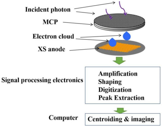
Figure 1.
Schematic diagram of XS detector structure.
A traditional signal processing system includes charge-sensitive amplifiers (CSAs), Gaussian shaping amplifiers, analog-to-digital converters (ADCs), and FPGA for signal acquisition, peak extraction, and data transmission, as shown in Figure 2. The output of the anode is a short-duration current pulse, which is converted into a negative exponential voltage signal by the CSA. A pole/zero cancellation circuit is used to shorten the long tail and correct the overshoot of the output pulse. In order to measure and extract the peak value, the CSA output is amplified and shaped into an approximate Gaussian voltage signal by the shaping amplifier. Subsequently, the Gaussian shaping amplifier output is digitized by the ADC and transmitted to FPGA for peak extraction. Finally, FPGA transmits the peak value of each channel to the computer through Ethernet. The purpose of Gaussian shaping amplifiers is not only to transform the shape of the CSA output pulse from a long tail pulse to a Gaussian curve, but also to filter much of the noise from the signal of interest. Generally, the longer the shaping time, the better the noise filtering effect [18]. The shaping time of amplifiers with satisfactory noise filtering capability is usually more than several hundred nanoseconds. However, in the case of high count rates, pulse pile-up with a long shaping time will become a problem, resulting in inaccuracies or even an inability to extract the peak. In recent years, advances in microelectronics enabled the CSA and shaping amplifiers to be combined into preamplifiers with fast shaping time and low noise. In 2006, researchers at the University of California at Berkeley developed a fully parallel signal processing system, in which the RD20 amplifier (~40 ns rise time, ~200 ns fall time, ~900 e RMS with the anode connected) with charge amplification and waveform shaping was used. This signal processing technique allows for high counting rates exceeding 1 MHz with the same high spatial resolution (<10 µm FWHM) [11,19]. After the development phase lasting more than ten years, the team’s researchers improved the performance of the XS detector to a spatial resolution of <20 µm at a >5 MHz counting rate [20,21]. The detection system with this architecture achieves excellent performance. However, in the case of a varying count rate, the fixed shaping time makes it unable to fully exert its advantages. For example, at low count rates, a system with a long shaping time will have lower noise than a system with a short shaping time. At a higher count rate, using a short shaping time at the expense of noise filtering performance can keep the detector working, without serious waveform superposition and data congestion.
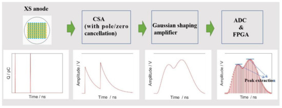
Figure 2.
Schematic diagram of the traditional signal processing system with analog Gaussian shaping amplifier and corresponding signal transmission model.
Therefore, a new signal processing system with digital trapezoidal shaping is proposed, as shown in Figure 3. Similar to the traditional architecture, the CSA is used to amplify the anode pulse. However, there is no Gaussian shaping amplifier, and the CSA output is directly digitized by the ADC and then transmitted to FPGA. The shaping and filtering are performed by the trapezoidal shaping filter in FPGA. The algorithm in FPGA can automatically adjust the shaping time according to the event time interval, maintaining good filtering performance at both high and low count rates. Compared with the traditional architecture, the new architecture not only simplifies the system components, but also extends the dynamic range of the detector.
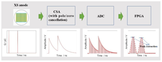
Figure 3.
Schematic diagram of the new signal processing system with digital trapezoidal shaping and corresponding signal transmission model.
3. Model Description
The arriving interval of photon events conforms to the Poisson distribution [22,23]; the probability of N electron clouds emanating from MCP stack in time t is derived:
where R is the average photon-counting rate, taking into account quantum efficiency. Depending on the bias voltage of the MCP, the total charge of the electron cloud conforms to Poisson or Gaussian distribution [24,25]. The broadening of the electron cloud has to be optimized to fit the size of the anode, which is related to the amount of charge, the distance, and the voltage between the MCP and the XS anode. A too-narrow charge footprint results in an under-sampled charge distribution. At the same time, a too-wide charge footprint leads to charge division between a large number of anode electrodes and, consequently, to the reduction in the signal-to-noise ratio. Generally, when the electron cloud covers 5–7 strips, the most accurate centroid calculation results can be obtained [13].
The anode strip output signal is a short-duration current pulse. The CSA converts this current pulse to a voltage pulse whose amplitude is proportional to the input charge. The CSA output pulse can be approximately mathematically represented as:
where τ is the decay time constant of the CSA output pulse. A is the amplitude of the CSA output pulse, which is proportional to the corresponding anode strip charge. The decay time depends on the combination of the feedback resistance and the integral capacitance, as well as the parameters of the pole/zero cancellation circuit. At a high count rate, the next pulse will be superimposed on the tail of the previous pulse, making the accurate extraction of pulse amplitude more difficult. To prevent the pulse pile-up, a CSA with a short decay time (80 ns) is selected.
Then, the CSA output pulse is digitized by a 12 bit ADC with a 62.5 MSPS sampling rate. Subsequently, a voltage variation corresponding to the noise of the front end of the detector is added/subtracted to the pulse in each channel. The noise at the front end of the detector mainly includes charge amplifier noise, charge division noise, capacitance noise, and ADC quantization noise, etc. The total noise can be generated according to the Gaussian distribution for a given RMS value by a random number generator.
The digitized CSA pulse is input into FPGA to be shaped and filtered into a trapezoidal pulse. The structure of the digital trapezoidal shaping filter is shown in Figure 4. It is composed of four modules (DS1, DS2, HPD, and ACC2) [26,27]. M is the time constant of the input pulse. For two superimposed pulses with an interval of 20 samples (320 ns), the filtered waveform is shown in Figure 5, where tp is the rise time and tft is the flat-top time of the trapezoid-shaped pulse. The total duration of trapezoidal waveform is defined as ts = 2 × tp + tft. The output waveform of different rise time tp and flat-top time tft can be obtained by changing the delay parameters l and k (in Figure 4).
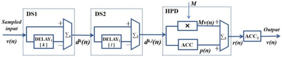
Figure 4.
Block diagram of the digital trapezoidal shaper. The elements are: DELAYn—a delay pipeline, ∑n—an adder/ subtracter, ACCn—an accumulator, and Xn—a multiplier.
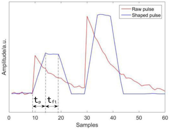
Figure 5.
Input waveform with noise and trapezoidal-shaped wave.
The point spread function (PSF) is used to characterize the overall resolution of the XS detector. The flow chart of the resolution measurement simulation is shown in Figure 6. At a single point with a fixed coordinate, a continuous electron cloud is generated randomly according to the distribution of time interval and amplitude. All the electron clouds are divided and integrated by the anode strips. Then, the charge on the anode is converted into digital voltage pulse by the CSA and the ADC. Subsequently, the signal is shaped and filtered by the trapezoidal shaping filter in FPGA and the peak value is extracted. Finally, the peak value is input to the computer for centroiding and mapping into an image. The position of the photon centroid is calculated using a modified center of gravity algorithm [13,28]. The distribution of calculated centroid coordinates is counted to obtain the point spread function.
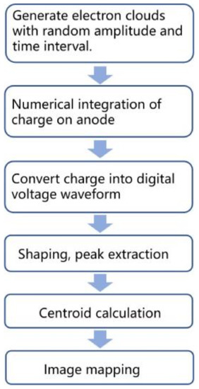
Figure 6.
Flow chart of resolution measurement simulation.
4. Simulation Results
4.1. Setting of Shaping Parameters
Two CSA waveforms with an interval of 100 samples are input into the trapezoidal filter. The output waveforms of different filtering parameters are shown in Figure 7a. When the flat-top time is set to 0, the filtered waveform is a symmetrical triangular waveform, and the total duration of the waveform is ts = 2 × tp. When ts is less than the time interval Ti, the output waveform is not superimposed. When ts is equal to or greater than half of Ti, the output waveform begins to overlap, but has no impact on the peak value. When ts is equal to or greater than Ti, the peak value cannot be accurately extracted, due to superposition. The longer the shaping time, the larger the corresponding output waveform amplitude. This will not affect the centroid calculation result because the input waveform of the same event passes through filters with the same parameters, so the relative value of each output waveform will not change.
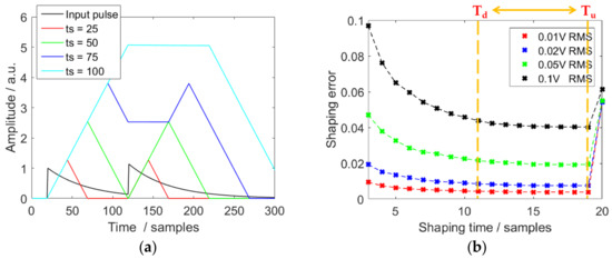
Figure 7.
(a) The output waveform of the same input waveform through filters with different parameters. The time interval is 100 samples (16 ns/sample), the flat-top time is 0, and the rise time is 25, 50, 75, and 100 samples, respectively. (b) Variation in shaping error with shaping times for different noise RMS.
One of the main purposes of shaping is to filter the noise. The following methods can be used to quantify the noise filtering effect. For two superimposed waveforms with the same amplitude at fixed time interval, the peak value is extracted after shaping by filter, which is recorded as P. Then, the input waveform is added with noise. After the same shaping operation as above, the peak value is extracted and recorded as Pn. The effect of noise filtering can be characterized by the difference between the P and Pn. Therefore, the shaping error can be defined as:
where Pn and P are the peaks that are extracted by shaping the input waveforms with and without noise using the same shaper, respectively. For the input waveform with an interval of 20 samples, a variation in the shaping error with shaping parameters under different noises is shown in Figure 7b, where Ti is 20 samples (16 ns/sample), the input pulse amplitude is 1 V, and tft = 0. As can be seen, when ts is less than Tit, the shaping error Es decreases with the increase in shaping time (ts = 2 ∗ tp). According to the shape of the curve, the change in the shaping error can be divided into three regions. When the shaping time is less than Td, the shaping error decreases rapidly with the increase in ts. The greater the noise of the waveform, the more obviously the curve will decline. When ts is greater than Td and less than Tu, the shaping error changes slowly. When ts is equal to or greater than Tu, the error increases sharply. This is because the shaped pulses are superimposed, resulting in the inability to accurately extract the peak value. Therefore, if the shaping time is set within a certain range (between Td and Tu), the shaper can achieve the best noise filtering effect.
Because of the Poisson distribution of photon intervals, a fixed ts cannot maintain the best noise filtering effect for all input waveforms. Therefore, we propose an adaptive filtering strategy that automatically sets filtering parameters according to the pulse interval in the sampling window. According to the photon count rate of the work area, a number of filters with different shaping parameters are preset. During data acquisition, the appropriate shaper is automatically used according to the photon intervals. Compared to the shaping strategy with fixed parameters, this adaptive filtering shaping method can not only avoid a high overlapping rate, but also give full play to the shaping performance. The relationship between the shaping error Es of different shaping strategies and the counting rate is shown in Figure 8. As can be seen, the filter with a small ts is less affected by the count rate, but the overall performance is mediocre. The shaper with a large ts performs well at a low count rate, while Es rises sharply due to superposition at a high count rate. Adaptive filtering can maintain the best performance at any count rate.
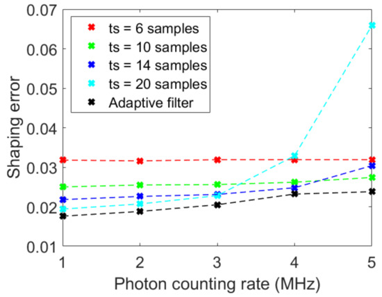
Figure 8.
Variation in the shaping error with photon-counting rate for different shaping strategies. The fixed ts is 6, 10, 14, and 20 samples (16 ns/sample), respectively. The input pulse amplitude is 1 V, noise is 0.05 V RMS, and tft = 0.
4.2. Point Spread Function
Noise and the photon-counting rate are two important factors affecting the filtering effect and the detector spatial resolution. In order to study the influence of counting rate and noise on spatial resolution, the PSF under different experimental conditions is measured. The photon position distribution at 5 MHz photon count rate and 500 e RMS noise is shown in Figure 9. The photon position distribution can be fitted as a two-dimensional Gaussian distribution, which is the PSF of photons. The full-width at half maximum (FWHM) of the PSF represents the imaging resolution of the detector. The relationship between FWHM and the photon-counting rate under different noise conditions is shown in Figure 10. It can be seen that FWHM increases with the increase in the count rate. At the same photon-counting rate, the greater the noise, the greater the FWHM, which means lower spatial resolution. At the photon count rate of 6 MHz, the spatial resolution of <50 μm can be achieved for a noise of 1000 e RMS. If the electronic noise can be reduced to 500 e RMS, the detector will reach <15 μm resolution at the 3 MHz count rate. It should be noted that the simulation in this paper is the detection of a single target point. When the actual detector with a certain area works, the photons will not fall at the same position each time, so the overall counting rate that can be achieved will be higher than this result. In addition to verifying the feasibility of this architecture, this model can be used as a guide in the process of detector design and optimization. We can design and optimize different detector parameters according to the target detection requirements.
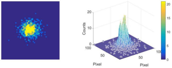
Figure 9.
The photon position distribution obtained by detector imaging at the 5 M photon count rate and 500 e RMS noise.
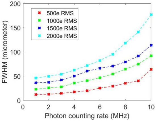
Figure 10.
Variation in FWHM with photon-counting rates for different noise RMS.
5. Conclusions
This paper proposes a new electronic signal processing scheme, which uses a digital trapezoidal shape filter instead of a Gaussian shaping amplifier. For the superimposed waveform, the influence of shaping parameters on the shaping error and the influence of the photon-counting rate and noise on the spatial resolution are studied. An adaptive digital trapezoidal filter that automatically selects the shaping parameters according to the pulse interval in the sampling window is proposed, and the detector imaging model is established to test the resolution. The imaging simulation results show that the detector with this scheme has a high dynamic range, and can still achieve a spatial resolution of <50 μm at a photon-counting rate of >6 MHz for a noise of 1000 e RMS. The new detector will have great applications in the large dynamic range of photon intensity scenes, such as 3D situation awareness or aurora detection.
Author Contributions
Conceptualization, Z.J.; Software, Z.J.; Validation, Z.J.; Data curation, Z.J.; Writing—original draft, Z.J.; Writing—review & editing, Z.J.; Supervision, Q.N.; Project administration, Q.N.; Funding acquisition, Q.N. All authors have read and agreed to the published version of the manuscript.
Funding
This work was supported by the National Natural Science Foundation of China under grant no. 62135015.
Institutional Review Board Statement
Not applicable.
Informed Consent Statement
Not applicable.
Data Availability Statement
Not applicable.
Conflicts of Interest
The authors declare no conflict of interest.
References
- Oelsner, A.; Schmidt, O.; Schicketanz, M. Microspectroscopy and imaging using a delay line detector in time-of-flight photoemission microscopy. Rev. Sci. Instrum. 2001, 72, 3968–3974. [Google Scholar] [CrossRef]
- Tremsin, A.S.; Siegmund, O.; Hull, J.S. High Resolution Photon Counting Detection System for Advanced Inelastic X-ray Scattering Studies. In Proceedings of the 2006 IEEE Nuclear Science Symposium Conference Record, San Diego, CA, USA, 29 October–4 November 2006; pp. 735–773. [Google Scholar]
- Shikhaliev, P.M.; Molloi, S. Count rate and dynamic range of an x-ray imaging system with mcp detector. Nucl. Instrum. Methods Phys. Res. A 2006, 557, 501–509. [Google Scholar] [CrossRef]
- Lees, J.E.; Pearson, J.F. A large area mcp detector for x-ray imaging. Nucl. Instrum. Methods Phys. Res. A 1997, 384, 410–424. [Google Scholar] [CrossRef]
- Zhang, X.; Chen, B. Wide-field auroral imager onboard the Fengyun satellite. Light. Sci. Appl. 2019, 45, 3957–3960. [Google Scholar] [CrossRef]
- Diebold, S.; Barnstedt, J.; Hermanutz, S. UV MCP Detectors for WSO-UV: Cross Strip Anode and Readout Electronics. IEEE Trans. Nucl. Sci. 2013, 60, 918–922. [Google Scholar] [CrossRef]
- Conti, L.; Barnstedt, J.; Buntrock, S.; Diebold, S.; Schaadt, D.M. Microchannel-Plate Detector Development for Ultraviolet Missions. In Proceedings of the SPIE Conference, Astronomical Telescopes and Instrumentation, Online, 14–18 December 2020. [Google Scholar]
- Conti, L.; Barnstedt, J.; Hanke, L.; Kalkuhl, C.; Kappelmann, N.; Rauch, T.; Stelzer, B.; Werner, K.; Elsener, H.-R.; Schaadt, D.M. MCP detector development for uv space missions. Astrophys. Space Sci. 2018, 363, 63. [Google Scholar] [CrossRef]
- Siegmund, O.; Vallerga, J.V.; Mcphate, J.B.; Tremsin, A.S. Next generation microchannel plate detector technologies for UV astronomy. Proc. SPIE Int. Soc. Opt. Eng. 2004, 5488, 789–800. [Google Scholar]
- Siegmund, O. High-performance microchannel plate detectors for UV/visible astronomy. Nucl. Inst. Methods Phys. Res. A 2004, 525, 12–16. [Google Scholar] [CrossRef]
- Tremsin, A.S.; Siegmund, O.; Vallerga, J.V.; Hull, J.S. Novel high resolution readout for uv and x-ray photon counting detectors with microchannel plates. Proc. SPIE–Int. Soc. Opt. Eng. 2006, 6276. [Google Scholar] [CrossRef]
- Tremsin, A.S.; Siegmund, O.; Vallerga, J.V.; Raffanti, R.; Weiss, S.; Michalet, X. High speed multichannel charge sensitive data acquisition system with self-triggered event timing. IEEE Trans. Nucl. Sci. 2009, 56, 1148–1152. [Google Scholar] [CrossRef]
- Jiang, Z.; Ni, Q. Design and Performance of Photon Imaging Detector Based on Cross-Strip Anode with Charge Induction. Appl. Sci. 2022, 12, 8471. [Google Scholar] [CrossRef]
- Seljak, A.; Cumming, H.S.; Varner, G.; Vallerga, J.; Raffanti, R.; Virta, V. A fast, low power and low noise charge sensitive amplifier asic for a uv imaging single photon detector. J. Instrum. 2017, 12, T04007. [Google Scholar] [CrossRef]
- Vallerga, J.; Mcphate, J.; Tremsin, A.; Siegmund, O.; Varner, G. Development of a flight qualified 100 × 100 mm MCP UV detector using advanced cross strip anodes and associated ASIC electronics. In SPIE Astronomical Telescopes + Instrumentation. Space Telescopes and Instrumentation 2016: Ultraviolet to Gamma Ray, Edinburgh, UK; SPIE: Bellingham, WS, USA, 2016. [Google Scholar]
- Pfeifer, M.; Diebold, S.; Barnstedt, J.; Hermanutz, S.; Kalkuhl, C.; Kappelmann, N. Low power readout electronics for a uv mcp detector with cross strip anode. J. Instrum. 2014, 9, 705–710. [Google Scholar] [CrossRef]
- Pfeifer, M.; Barnstedt, J.; Diebold, S.; Hermanutz, S.; Werner, K. Characterisation of low power readout electronics for a UV microchannel plate detector with cross-strip readout. SPIE Astron. Telesc. Instrum. 2016, 9144, 914438. [Google Scholar]
- Ni, Q. Optimization for spatial resolution and count rate of a far ultraviolet photon-counting imaging detector based on induced charge position-sensitive anode. Acta Opt. Sin. 2014, 34, 0804001. [Google Scholar]
- Siegmund, O.; Tremsin, A.S.; Vallerga, J.V. High Performance Cross-Strip Detector Technologies for Space Astrophysics; IEEE Nuclear Science Symposium Conference Record: Honolulu, HI, USA, 2007. [Google Scholar]
- Vallerga, J.; Raffanti, R.; Cooney, M.; Cumming, H.; Varner, G.; Seljak, A. Cross Strip Anode Readouts for Large Format, Photon Counting Microchannel Plate Detectors: Developing Flight Qualified Prototypes of the Detector and Electronics; International Society for Optics and Photonics: Montréal, QB, Canada, 2014; Volume 9144, pp. 1090–1101. [Google Scholar]
- Siegmund, O.; Mcphate, J.; Curtis, T.; Darling, N.; Ertley, C. Development of UV imaging detectors with atomic layer deposited microchannel plates and cross strip readouts. In X-ray, Optical, and Infrared Detectors for Astronomy IX; SPIE: Bellingham, WS, USA, 2020. [Google Scholar]
- Omote, K. Dead-time effects in photon counting distributions. Nucl. Instrum. Methods Phys. Res. B 1990, 293, 582–588. [Google Scholar] [CrossRef]
- Cretot-Richert, G.; Francoeur, M. Applications Expand for Photon Counting. Photonics Spectra 2014, 48, 43–46. [Google Scholar]
- Saito, M.; Saito, Y.; Mukai, T.; Asamura, K. Spatial charge cloud size of microchannel plates. Rev. Sci. Instrum. 2007, 78, 023302. [Google Scholar] [CrossRef]
- Ni, Q.; Song, K.; Liu, S. Curved focal plane extreme ultraviolet detector array for a EUV camera on CHANG E lander. Opt. Express 2015, 23, 30755–30766. [Google Scholar] [CrossRef]
- Jordanov, V.T.; Knoll, G.F.; Huber, A.C.; Pantazis, J.A. Digital techniques for real-time pulse shaping in radiation measurements. Nucl. Instrum. Methods Phys. Res. 1994, 353, 261–264. [Google Scholar] [CrossRef]
- Jordanov, V.T.; Knoll, G.F. Digital synthesis of pulse shapes in real time for high resolution radiation spectroscopy. Nucl. Instrum. Methods Phys. Res. 1994, 345, 337–345. [Google Scholar] [CrossRef]
- Tremsin, A.S.; Vallerga, J.V.; Siegmund, O.; Hull, J.S. Centroiding algorithms and spatial resolution of photon counting detectors with cross-strip anodes. Proc. SPIE Int. Soc. Opt. Eng. 2003, 5164, 113–124. [Google Scholar]


Disclaimer/Publisher’s Note: The statements, opinions and data contained in all publications are solely those of the individual author(s) and contributor(s) and not of MDPI and/or the editor(s). MDPI and/or the editor(s) disclaim responsibility for any injury to people or property resulting from any ideas, methods, instructions or products referred to in the content. |
© 2023 by the authors. Licensee MDPI, Basel, Switzerland. This article is an open access article distributed under the terms and conditions of the Creative Commons Attribution (CC BY) license (https://creativecommons.org/licenses/by/4.0/).