Featured Application
This work provides an effective and promising strategy for the protection of optoelectronic systems against electromagnetic interference.
Abstract
Metal mesh films have been shown to be a promising strategy to effectively mitigate the growing issue of electromagnetic interference (EMI) in optoelectronic systems. To achieve superior shielding effectiveness, it is common to increase the thickness of the mesh film. However, mesh-based shielding materials have frequency-dependent shielding effectiveness that decreases as the frequency increases. Simply increasing the thickness of the mesh cannot effectively enhance the EMI shielding effectiveness at high frequencies. This will further lead to challenges such as increased processing difficulties and higher costs. In this paper, we present an infrared transparent electromagnetic shielding window based on metal mesh with irregular patterns and proper thickness. The mesh coating is fabricated on a sapphire substrate using ultraviolet photolithography technology and exhibits an efficient electromagnetic shielding effectiveness of more than 20 dB over the wide frequency range of 1.7–18 GHz while maintaining high infrared optical transparency. More importantly, there is no distinct variation in shielding effectiveness between low and high frequency ranges, demonstrating a balanced shielding characteristic across a broad frequency band. This work could be crucial in designing cost-effective and efficient EMI shielding windows for optoelectronic systems.
1. Introduction
With the rapid advancement of electronics and wireless communications, electromagnetic radiation generated by the operation of various electronic and electrical equipment and related infrastructure is becoming increasingly ubiquitous in space. The radiation is broadening in frequency spectrum and intensity, leading to a more complex electromagnetic environment [1,2]. Electromagnetic interference (EMI) that ensues from disorderly, high-intensity electromagnetic radiation can disrupt the normal operation of electronic information systems [3]. Notably, optoelectronic systems are particularly vulnerable to EMI due to their sophisticated optical sensors, photoelectric conversion modules, and integrated circuits [4,5]. An effective approach to protecting such systems from electromagnetic radiation is integrating electromagnetic functional materials into the optical windows [6] which serve as the primary channel for the radiation to enter the system.
EMI shielding materials used in optical windows of optoelectronic systems must provide both efficient protection against microwave radiation and high transparency for high-quality detection and imaging [7,8,9]. While most researches on transparent EMI shielding materials have been focused on visible light transmission, the rising demand for infrared optoelectronic systems in the military, aerospace, and other fields highlight the need for the development of infrared transparent electromagnetic shielding windows [10]. Common strategies for achieving infrared transparent electromagnetic shielding include the application of ultra-thin metal films or metal mesh films to the outer surfaces of the windows or the utilization of infrared transparent conductive oxides [11,12,13,14,15,16]. Additionally, some novel materials, such as carbon nanomaterials, have demonstrated favorable conductive and infrared optical properties as well [10,17].
Continuous or quasi-continuous transparent conducting films such as transparent conductive oxides, ultra-thin metals, and films of carbon nanotubes can provide efficient EMI shielding effectiveness (SE) [18,19,20]. However, a well-known issue with these films is that their transparency is compromised as the loading amount or film thickness increases [21,22]. As a result, it is difficult to decouple the optical transmittance from the EMI SE. One solution to this problem is the use of perforated metallic micro-structures or networks, such as metallic meshes, which can partially alleviate the conflict between optical transmittance and electrical conductivity by increasing the mesh thickness [23]. Metallic meshes with micron/submicron line widths and submillimeter grid spacings have been demonstrated to effectively transmit high levels of Vis-IR light while simultaneously reflecting microwaves [24,25]. In these materials, the void aperture allows for optical transparency while the interconnected fine metallic wires provide electrical conductivity.
While the main focus is on EMI shielding effectiveness, it is important to consider the shielding frequency spectrum as well, especially in the case of broadband EMI shielding. Mesh-based shielding materials often exhibit frequency-dependent shielding effectiveness, with the effectiveness decreasing as the frequency increases [23,24,26]. As a result, the shielding effectiveness of metal meshes over a wide frequency range is commonly evaluated by their performance at high frequencies. To achieve superior shielding effectiveness, it is customary to increase the thickness of the mesh film. Nevertheless, this practice is not without challenges. For instance, although increasing the thickness of the mesh can lead to a certain degree of improvement in shielding effectiveness at low frequencies, the enhancement at high frequencies is limited, resulting in a significant difference between the shielding effectiveness of high and low frequency bands. Furthermore, the intricate micro- and nano-processing procedures involved in the preparation of the metallic mesh make excessive thickness a hindrance, leading to increased processing difficulties and costs. Highly efficient mesh-based EMI shielding materials have still been underachieving.
It is expected that outstanding overall performance can be realized by engineering and optimizing the structural parameters, i.e., materials, density, mesh pattern, linewidth, spacing, and particularly the film thickness. In this study, we developed an IR transparent EMI shielding window that uses thin metallic meshes to provide efficient and stable EMI shielding properties over a broad frequency spectrum. The irregular polygonal metallic meshes with optimized dimensional parameters were fabricated on a sapphire substrate and exhibited efficient EMI shielding effectiveness of more than 20 dB in the wide frequency range of 1.7–18 GHz while maintaining high optical transparency in the infrared range. Additionally, the shielding effectiveness did not significantly decline in the high frequency range, indicating a balanced shielding property over a wide frequency spectrum. Our results also suggest that mesh thickness is a critical parameter that impacts EMI shielding properties over a wide range of frequencies. This work has important implications for the protection of infrared optoelectronic systems from electromagnetic interference in practical applications.
2. Design and Methods
2.1. Structure Design of Transparent EMI Shielding Window
The sheet resistance of a conductive film provides a reliable measure of its EMI shielding ability and can be determined by the skin depth (δ) and thickness (t) of the thin film [27]. The skin depth is defined as [28]:
where μ and σ are the permeability and conductivity of the film, respectively. Usually, the thickness of the metal mesh film is designed to be greater than the skin depth in order to obtain higher shielding effectiveness. However, increasing the thickness only improves shielding performance at low frequencies [9]. For the mesh coating with a thickness much less than the skin depth, the SE is dominated by the reflection of the incident plane wave at the air-mesh interface. When the skin depth decreases, the shielding effectiveness also decreases accordingly [29]. However, the skin depth of a conductive film decreases as the frequency gets higher. A thicker metal mesh can reduce the sheet resistance of the mesh coating and enhance the EMI shielding performance at lower frequencies [30]. However, it contributes a little to the improvement of EMI SE at higher frequencies. Based on a comprehensive consideration of the effects of mesh aperture structure, sheet resistance, and skin depth on shielding effectiveness, it is possible to alleviate the frequency dependence of shielding effectiveness by designing the proper mesh thickness for achieving a balanced shielding effectiveness in a wide frequency band. In this study, the mesh thickness is several hundred nanometers, much thinner than the skin depth of the metallic film.
The transparent EMI shielding window, shown schematically in Figure 1a, is composed of a sapphire substrate and two layers of metal mesh films on its surface. Sapphire is chosen for its excellent physical properties, including high infrared transparency, good thermal conductivity, high hardness, and the ability to withstand high temperatures [31]. The thickness of the Au mesh layer is designed to be between 200 and 300 nm, which is sufficient to provide good conductivity for effective microwave reflection. The Cr mesh is used as the adhering layer and is much thinner than the Au mesh. In addition to the mesh-based shielding films, a layer of Al2O3 is used as a covering layer to protect the mesh film from erosion in harsh environments.
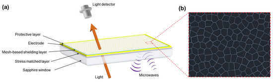
Figure 1.
Design of the IR transparent EMI shielding window. (a) Schematical illustration of the structure design and function of IR transparency and microwave reflection. (b) Mesh pattern of irregular polygons.
The design of the mesh pattern can significantly impact the optical properties of transparent shielding materials. Conventional meshes, such as square metal grids, tend to produce poor imaging quality due to centralized diffraction distribution [32]. To reduce the concentration of high-order diffraction and minimize the impact of imaging caused by the mesh shielding layer, the metal mesh is designed with irregular patterns, as shown in Figure 1b. The irregular mesh patterns are designed with an equivalent period of 110 μm and a linewidth of 2.5 μm, which allows for high IR transmittance due to the reduced obscuration ratio.
2.2. Materials and Fabrication
Metallic mesh films can be fabricated using various methods, including photolithography [26,33], printing [34,35], nano-imprinting [36], and laser direct-writing technology [29]. To obtain meshes with fine lines, a mature process of ultraviolet (UV) photolithography was adopted in this study to prepare the samples. The specific fabricating process is illustrated in Figure 2a. First, positive photoresist (AZ 5214E) was spin-coated onto the cleaned sapphire substrate. Then, photoresist film (~2 μm in thickness) with mesh patterns was obtained after exposure and the development process. Afterwards, metal films (Cr/Au) were routinely deposited by a magnetron sputtering system (PVD75, Kurt J. Lesker) in the presence of argon with a base pressure of 3.0 × 10⁻⁶ Torr. Cr and Au deposition rates were 0.66 Å/s and 1.00 Å/s, respectively. The thin Cr mesh layer is provided for better adhesion of the grid layer to the sapphire substrate. The photoresist was then dissolved to reveal the metal meshes in accordance with the designed mesh pattern. Figure 2b shows the micrograph of metallic meshes under a magnification of 50×. It can be observed that the metallic wires are continuous and have no fractures, which ensures that the mesh coating has good electrical conductivity. According to Figure 2c, the average linewidth of the mesh is measured to be ~2.5 μm. The photolithography technology adopted in this work has high precision and can obtain narrow linewidths, resulting in minimal loss of transparency. Additionally, the process is stable, highly reproducible, and capable of batch production.
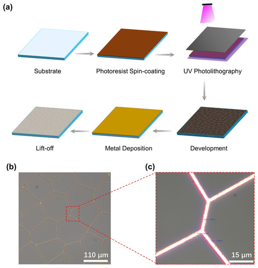
Figure 2.
(a) Fabricating process of the IR transparent EMI shielding window. (b) Micrograph of metallic meshes under magnification of 50×. (c) Measurement of linewidth under magnification of 400×.
3. Results and Discussion
The optical transmittance of the sample in the mid-wave IR region (3–5 μm) was measured using a Fourier transform infrared spectrometer (FTIR-650S, Gangdong Sci & Tech, Tianjin, China) under ambient conditions. The IR transmittances of the bare sapphire window, the sapphire window with mesh coatings, and the sapphire window with mesh coatings and the covering layer are plotted in Figure 3. It can be seen that the bare sapphire window itself is highly transparent to IR light, exhibiting a high transmittance of 88.89% at 3.210 μm. Since the mesh has large effective apertures for light transmission, the infrared transmittance of the window decreased by only 4.14% after the mesh coating was fabricated. The most interesting aspect of the result is that the transmittance of the electromagnetic shielding window with a covering layer is slightly increased by 1.42% and reaches 86.17%, which can be attributed to the destructive interference [37]. As a result, the electromagnetic shielding layer reduces the window’s infrared transmittance by only 2.72%. With such a high transmission rate, the employment of the electromagnetic shielding window does not affect the detecting and imaging functions of optoelectronic system. It is worth noting that the IR transmittance starts to decrease at wavelengths greater than 4 μm and drops to ~48% at 5 μm. This is due to the increased IR absorption of Al2O3 in this region. In addition, it is worth mentioning that the transmission short-wave cutoff limit is about 0.19 μm [31]; the EMI shielding window possesses high visible light transmittance as well.
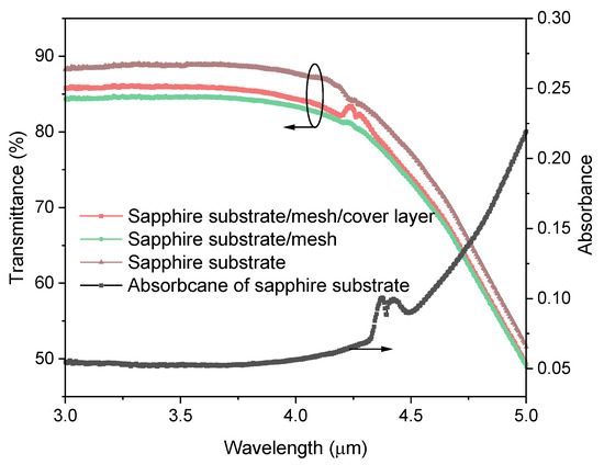
Figure 3.
Optical properties of the transparent EMI shielding window.
Attenuation of electromagnetic waves by shielding materials is quantified by shielding effectiveness, which is the logarithmic ratio of the incident power (Pi) to the transmitted power (Pt) [13]. Measurements of EMI shielding performance in this study were conducted over a wide frequency range of 1.7–18 GHz using the waveguide method [38], which is schematically illustrated in Figure 4a. The EMI shielding measurement setup consists mainly of a vector network analyzer (VNA, AV3672B, Ceyear, Qingdao, China) and waveguides, as shown in Figure 4b. The system was calibrated using the Transmission-Reflection-Load (TRL) technique before testing. As-prepared samples were firmly clamped between the commissures of waveguides, and different sets of waveguides operating in L-, S-, C-, X-, and Ku-band were utilized to achieve shielding performance across a broad frequency spectrum. EMI SE values can be obtained through S-parameters collected by the VNA. Since the ratio of Pi to Pt is the measure of electromagnetic transmittance, the total SE can be expressed as [13,29]:
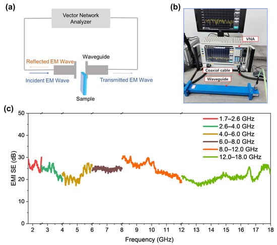
Figure 4.
EMI shielding performance. (a) Schematic illustration of EMI SE measuring method based on waveguides. (b) The actual EMI SE measurement setup. (c) Measured EMI SE of transparent electromagnetic shielding window over wide frequency range of 1.7–18 GHz.
According to transmission line theory, EMI Shielding effectiveness of a conductive film is mainly dependent on the sheet resistance [25], and the metallic mesh performs as a continuous conductive film at low frequencies. The sheet resistance of a mesh film can be controlled by the structural parameters of mesh thickness, period, and linewidth [39]. In this study, linewidth of the metal mesh is of 2.5 µm and the mesh period is 110 µm. The thickness of Cr and Au mesh layers are 35 nm and 285 nm, respectively. Figure 4c presents the measured EMI shielding performance of the mesh-coated sapphire window. The average EMI SE in the wide frequency range of 1.7–18 GHz is measured to be 23.5 dB, which can block more than 99% electromagnetic power and is sufficient for practical applications [40].
It has been reported that mesh film exhibits obvious EMI shielding degradation at higher frequencies [24,25,32,41,42]. What is different in this study is that the shielding performance of the mesh coating is balanced over a wide frequency range. For mesh coatings, the underlying cause of the frequency-dependent property of EMI shielding can be explained by analyzing the transmission (T) of electromagnetic waves, which can be expressed as follows in the case of normal incidence in free space [24]:
where y is the normalized admittance of the individual mesh film without a substrate. When the linewidth (w) of the mesh is larger than its thickness and much smaller than the period (p), the normalized admittance can be expressed as [24,43]:
where λ is the wavelength of the incident electromagnetic wave. According to Equation (4), as the frequency gets higher and the wavelength gets smaller, the normalized admittance of the conductive mesh decreases. Therefore, the metal mesh exhibits a decrease in shielding efficiency at higher frequencies. In addition to the influence of the aperture structure on the transmission coefficient of the mesh, the variation of the sheet resistance of the mesh with frequency is also an important reason for the frequency dependence of its shielding effectiveness. The frequency dependence of sheet resistance for mesh coatings can be described as follows [30]:
Here δ is the skin depth, σ is the conductivity of the metal, t, p, and w are the thickness, period, and linewidth of the mesh, respectively. As the frequency gets higher, the sheet resistance of the mesh film increases.
According to the measured result, the average EMI SE of L- to Ku-band are 25.5 dB, 23.1 dB, 23.6 dB, 24.4 dB, and 20.9 dB, respectively. It can be seen that EMI SE is only weakly dependent on frequency, demonstrating that the thin metal film is beneficial to alleviate the dependence of EMI SE on frequency. Additionally, the irregular mesh pattern design also contributes to the stable shielding property, which has been experimentally verified by Han et al. [23]. The thin meal mesh with irregular patterns in this study not only ensures effective EMI shielding performance, but also reduces the frequency dependence of the shielding effectiveness, which is beneficial to obtain a balanced shielding effectiveness in a wide frequency band. The advantage of adopting the thin mesh is that a more stable shielding performance can be achieved over a wide frequency band. In addition, the design of the thin mesh facilitates costly and time-consuming mesh fabricating process, making it possible to achieve the desired shielding performance in an efficient manner.
Figure 3a–f present the EMI shielding performance of metal meshes with different thicknesses in six measured frequency bands. One can see that the thickness variation has different effects on the shielding effectiveness in different frequency bands. A close inspection of the figures shows that the effect of thickness variation on shielding effectiveness is more evident at lower frequencies. In the frequency range of 1.7–2.6 GHz, the average EMI SE values of samples with thickness of 320 nm and 230 nm are 26.1 dB and 22.7 dB, respectively (Figure 5a). According to Figure 5f, however, the average EMI SE values of the two samples are 20.9 dB and 20.0 dB, showing that the effect of thickness variation on shielding effectiveness gradually weakens as the frequency increases. Specific EMI SE values of the samples in different frequency bands are obtained and summarized in Table 1. As the frequency gets higher, the difference in shielding effectiveness exhibited by mesh coatings with different thicknesses gradually decreases, indicating that the variation in mesh thickness has little effect on the shielding effectiveness at high frequencies.
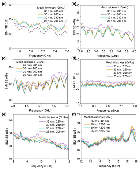
Figure 5.
EMI shielding performance of metallic meshes with different thickness in varying frequency band. (a) 1.7–2.6 GHz. (b) 2.6–4 GHz. (c) 4–6 GHz. (d) 6–8 GHz. (e) 8–12 GHz. (f) 12–18 GHz.

Table 1.
Summary of average SE of meshes with varying thickness in each frequency band.
In contrast to some transparent frequency selective surfaces (FSSs) based on periodic metal mesh, which can provide passbands for partial frequency bands and achieve high shielding effectiveness in narrower frequency bands [44,45,46], the metal mesh design in this work mainly emphasizes its stable shielding characteristics within a wide frequency band. To highlight this feature, a comparison of the variations in SE at different frequencies for representative reported shielding materials based on meshes is shown in Table 2. The mesh shape includes squares [24,26,42], hexagons [9], and irregular shapes [23], and the materials cover different metals and conductive oxides [47]. Although some works only provide the shielding performance of the material in one frequency band, one can see that the mesh-based transparent electromagnetic shielding materials generally exhibit significant shielding effectiveness fluctuations over a wide frequency band, especially the difference between high and low frequency bands. In [24], for example, the variation in shielding effectiveness between 4 GHz and 12 GHz for square copper meshes reaches 10 dB. In comparison, the difference in shielding effectiveness between these two frequency points is only 0.6 dB in our design. While the square Ti/Au/Ag mesh presented in [48] is thinner, the variation in shielding effectiveness at 12 GHz and 18 GHz is ~6 dB, which is still greater than that of this work. The overall variation in shielding effectiveness over a wide frequency band is small. More importantly, the thickness of the mesh is much thinner, which offers great processing convenience and cost advantages.
Table 2.
Comparison of SE variation at different frequency for various mesh films.
4. Conclusions
In summary, a metallic mesh-based transparent EMI shielding window with high IR transparency and balanced electromagnetic shielding performance across a wide frequency spectrum has been designed and fabricated. The mesh coating was fabricated on a sapphire window using UV photolithography, resulting in both a high IR transmittance of 85.1% and a favorable EMI SE of 23.5 dB. The shielding effectiveness was balanced across a wide frequency range and only weakly dependent on frequency. The optimization of EMI shielding performance through the variation of mesh film thickness was also demonstrated. This design has the added benefit of reducing the time-consuming and energy-intensive process of metal deposition typically required for the preparation of thick meshes, enabling the production of efficient transparent electromagnetic shielding materials with balanced wideband shielding performance. The combination of these characteristics makes the mesh-coated sapphire window an ideal EMI shielding component for optoelectronic systems.
Author Contributions
Conceptualization, X.H.; data curation, Y.L. and W.L.; formal analysis, Y.L. and X.H.; investigation, Y.L; methodology, J.P.; validation, Z.W., K.W., L.Y. and J.P.; supervision and project administration, X.H. and P.L.; writing—original draft, Y.L.; writing—review and editing, Z.W., K.W., L.Y. and X.H. All authors have read and agreed to the published version of the manuscript.
Funding
This research was funded by Huxiang Youth Talent Support Program, grant number 2020RC3028 and the National Natural Science Foundation of Hunan Province, grant number 2022JJ20045.
Institutional Review Board Statement
Not applicable.
Informed Consent Statement
Not applicable.
Data Availability Statement
Not applicable.
Conflicts of Interest
The authors declare no conflict of interest.
References
- Schroder, A.; Rasek, G.A.; Bruns, H.-D.; Reznicek, Z.; Kucera, J.; Loos, S.E.; Schuster, C. Analysis of High Intensity Radiated Field Coupling into Aircraft Using the Method of Moments. IEEE Trans. Electromagn. Compat. 2014, 56, 113–122. [Google Scholar] [CrossRef]
- Kim, S.; Oh, J.-S.; Kim, M.-G.; Jang, W.; Wang, M.; Kim, Y.; Seo, H.W.; Kim, Y.C.; Lee, J.-H.; Lee, Y.; et al. Electromagnetic Interference (EMI) Transparent Shielding of Reduced Graphene Oxide (RGO) Interleaved Structure Fabricated by Electrophoretic Deposition. ACS Appl. Mater. Interfaces 2014, 6, 17647–17653. [Google Scholar] [CrossRef] [PubMed]
- Geetha, S.; Kumar, K.K.S.; Rao, C.R.K.; Vijayan, M.; Trivedi, D.C. EMI Shielding: Methods and Materials-A Review. J. Appl. Polym. Sci. 2009, 112, 2073–2086. [Google Scholar] [CrossRef]
- Qin, F.; Yan, Z.; Fan, J.; Cai, J.; Zhu, X.; Zhang, X. Highly Uniform and Stable Transparent Electromagnetic Interference Shielding Film Based on Silver Nanowire-PEDOT:PSS Composite for High Power Microwave Shielding. Macromol. Mater. Eng. 2021, 306, 2000607. [Google Scholar] [CrossRef]
- Iqbal, A.; Shahzad, F.; Hantanasirisakul, K.; Kim, M.-K.; Kwon, J.; Hong, J.; Kim, H.; Kim, D.; Gogotsi, Y.; Koo, C.M. Anomalous absorption of electromagnetic waves by 2D transition metal carbonitride Ti3CNTx (MXene). Science 2020, 369, 446–450. [Google Scholar] [CrossRef]
- Fortuna, L.; Buscarino, A. Smart Materials. Materials 2022, 15, 6307. [Google Scholar] [CrossRef]
- Chen, W.; Liu, L.-X.; Zhang, H.-B.; Yu, Z.-Z. Flexible, Transparent, and Conductive Ti3C2Tx MXene-Silver Nanowire Films with Smart Acoustic Sensitivity for High-Performance Electromagnetic Interference Shielding. ACS Nano 2020, 14, 16643–16653. [Google Scholar] [CrossRef]
- Van Viet, T.; Duc Dung, N.; Nguyen, A.T.; Hofmann, M.; Hsieh, Y.-P.; Kan, H.-C.; Hsu, C.-C. Electromagnetic Interference Shielding by Transparent Graphene/ Nickel Mesh Films. ACS Appl. Nano Mater. 2020, 3, 7474–7481. [Google Scholar] [CrossRef]
- Liang, Y.; Huang, X.; Pan, J.; Liu, W.; Wen, K.; Zhai, D.; Shang, P.; Liu, P. Shorted Micro-Waveguide Array for High Optical Transparency and Superior Electromagnetic Shielding in Ultra-Wideband Frequency Spectrum. Adv. Mater. Technol. 2023, 2201532. [Google Scholar] [CrossRef]
- Han, J.; Wang, X.; Qiu, Y.; Zhu, J.; Hu, P. Infrared-transparent films based on conductive graphene network fabrics for electromagnetic shielding. Carbon 2015, 87, 206–214. [Google Scholar] [CrossRef]
- Sun, C.; Meng, Y.; Liu, X.; Wang, X.; Liu, Y.; Tan, J. Ring and circular aperture hexagonal array resonance micromesh coating with infrared dual-bandpass extraordinary transmission and strong electromagnetic shielding. Mater. Chem. Phys. 2019, 234, 323–328. [Google Scholar] [CrossRef]
- Fernandes, G.E.; Lee, D.-J.; Kim, J.H.; Kim, K.-B.; Xu, J. Infrared and microwave shielding of transparent Al-doped ZnO superlattice grown via atomic layer deposition. J. Mater. Sci. 2013, 48, 2536–2542. [Google Scholar] [CrossRef]
- Han, Y.; Liu, Y.; Han, L.; Lin, J.; Jin, P. High-performance hierarchical graphene/metal-mesh film for optically transparent electromagnetic interference shielding. Carbon 2017, 115, 34–42. [Google Scholar] [CrossRef]
- Ghosh, D.S.; Martinez, L.; Giurgola, S.; Vergani, P.; Pruneri, V. Widely transparent electrodes based on ultrathin metals. Opt. Lett. 2009, 34, 325–327. [Google Scholar] [CrossRef] [PubMed]
- Ulrich, R. Far-infrared properties of metallic mesh and its complementary structure. Infrared Phys. 1967, 7, 37–55. [Google Scholar] [CrossRef]
- Menon, A.V.; Jagadeshvaran, P.L.; Bose, S. Geometry and mesh size control the EMI shielding in 3D printed conducting shape memory PU structures. J. Mater. Chem. C 2023, 11, 4474–4485. [Google Scholar] [CrossRef]
- Hu, L.; Hecht, D.S.; Gruner, G. Infrared transparent carbon nanotube thin films. Appl. Phys. Lett. 2009, 94. [Google Scholar] [CrossRef]
- Zhang, C.; Ji, C.; Park, Y.-B.; Guo, L.J. Thin-Metal-Film-Based Transparent Conductors: Material Preparation, Optical Design, and Device Applications. Adv. Opt. Mater. 2021, 9, 2001298. [Google Scholar] [CrossRef]
- Wan, Y.-J.; Zhu, P.-L.; Yu, S.-H.; Sun, R.; Wong, C.-P.; Liao, W.-H. Anticorrosive, Ultralight, and Flexible Carbon-Wrapped Metallic Nanowire Hybrid Sponges for Highly Efficient Electromagnetic Interference Shielding. Small 2018, 14, 1800534. [Google Scholar] [CrossRef]
- Wang, Y.-Y.; Zhou, Z.-H.; Zhou, C.-G.; Sun, W.-J.; Gao, J.-F.; Dai, K.; Yan, D.-X.; Li, Z.-M. Lightweight and Robust Carbon Nanotube/Polyimide Foam for Efficient and Heat-Resistant Electromagnetic Interference Shielding and Microwave Absorption. ACS Appl. Mater. Interfaces 2020, 12, 8704–8712. [Google Scholar] [CrossRef]
- Zhu, X.; Xu, J.; Qin, F.; Yan, Z.; Guo, A.; Kan, C. Highly efficient and stable transparent electromagnetic interference shielding films based on silver nanowires. Nanoscale 2020, 12, 14589–14597. [Google Scholar] [CrossRef]
- Yuan, C.; Huang, J.; Dong, Y.; Huang, X.; Lu, Y.; Li, J.; Tian, T.; Liu, W.; Song, W. Record-High Transparent Electromagnetic Interference Shielding Achieved by Simultaneous Microwave Fabry-Perot Interference and Optical Antireflection. ACS Appl. Mater. Interfaces 2020, 12, 26659–26669. [Google Scholar] [CrossRef]
- Han, Y.; Lin, J.; Liu, Y.; Fu, H.; Ma, Y.; Jin, P.; Tan, J. Crackle template based metallic mesh with highly homogeneous light transmission for high-performance transparent EMI shielding. Sci. Rep. 2016, 6, 25601. [Google Scholar] [CrossRef]
- Tung, P.D.; Jung, C.W. High Optical Visibility and Shielding Effectiveness Metal Mesh Film for Microwave Oven Application. IEEE Trans. Electromagn. Compat. 2020, 62, 1076–1081. [Google Scholar] [CrossRef]
- Voronin, A.S.; Fadeev, Y.V.; Govorun, I.V.; Podshivalov, I.V.; Simunin, M.M.; Tambasov, I.A.; Karpova, D.V.; Smolyarova, T.E.; Lukyanenko, A.V.; Karacharov, A.A.; et al. Cu-Ag and Ni-Ag meshes based on cracked template as efficient transparent electromagnetic shielding coating with excellent mechanical performance. J. Mater. Sci. 2021, 56, 14741–14762. [Google Scholar] [CrossRef]
- Han, Y.; Zhong, H.; Liu, N.; Liu, Y.; Lin, J.; Jin, P. In Situ Surface Oxidized Copper Mesh Electrodes for High-Performance Transparent Electrical Heating and Electromagnetic Interference Shielding. Adv. Electron. Mater. 2018, 4, 1800156. [Google Scholar] [CrossRef]
- Maniyara, R.A.; Mkhitaryan, V.K.; Chen, T.L.; Ghosh, D.S.; Pruneri, V. An antireflection transparent conductor with ultralow optical loss (<2 %) and electrical resistance (<6 Ω sq−1). Nat. Commun. 2016, 7, 13771. [Google Scholar] [CrossRef]
- Kuzhir, P.P.; Paddubskaya, A.G.; Maksimenko, S.A.; Kaplas, T.; Svirko, Y. Microwave absorption properties of pyrolytic carbon nanofilm. Nanoscale Res. Lett. 2013, 8, 60. [Google Scholar] [CrossRef]
- Zhang, Y.; Dong, H.; Li, Q.; Mou, N.; Chen, L.; Zhang, L. Double-layer metal mesh etched by femtosecond laser for high-performance electromagnetic interference shielding window. RSC Adv. 2019, 9, 22282–22287. [Google Scholar] [CrossRef]
- Liu, Y.; Tan, J. Frequency dependent model of sheet resistance and effect analysis on shielding effectiveness of transparent conductive mesh coatings. Prog. Electromagn. Res.-Pier 2013, 140, 353–368. [Google Scholar] [CrossRef]
- Tropf, W.J.; Thomas, M.E.; Klocek, P. Infrared optical materials. Inorg. Opt. Mater. A Crit. Rev. 1996, 10286, 93–125. [Google Scholar] [CrossRef]
- Wang, W.; Bai, B.; Zhou, Q.; Ni, K.; Lin, H. Petal-shaped metallic mesh with high electromagnetic shielding efficiency and smoothed uniform diffraction. Opt. Mater. Express 2018, 8, 3485–3493. [Google Scholar] [CrossRef]
- Qi, L.; Li, J.; Zhu, C.; Yang, Y.; Zhao, S.; Song, W. Realization of a flexible and mechanically robust Ag mesh transparent electrode and its application in a PDLC device. RSC Adv. 2016, 6, 13531–13536. [Google Scholar] [CrossRef]
- Li, H.; Zhang, Y.; Tai, Y.; Zhu, X.; Qi, X.; Zhou, L.; Li, Z.; Lan, H. Flexible transparent electromagnetic interference shielding films with silver mesh fabricated using electric-field-driven microscale 3D printing. Opt. Laser Technol. 2022, 148, 107717. [Google Scholar] [CrossRef]
- Li, Z.; Li, H.; Zhu, X.; Peng, Z.; Zhang, G.; Yang, J.; Wang, F.; Zhang, Y.F.; Sun, L.; Wang, R. Directly printed embedded metal mesh for flexible transparent electrode via liquid substrate electric-field-driven jet. Adv. Sci. 2022, 9, 2105331. [Google Scholar] [CrossRef]
- Chen, X.; Nie, S.; Guo, W.; Fei, F.; Su, W.; Gu, W.; Cui, Z. Printable High-Aspect Ratio and High-Resolution Cu Grid Flexible Transparent Conductive Film with Figure of Merit over 80,000. Adv. Electron. Mater. 2019, 5, 1800991. [Google Scholar] [CrossRef]
- Zhang, J.; Wu, H.; Jiao, H.; Schroeder, S.; Trost, M.; Wang, Z.; Cheng, X. Reducing light scattering in high-reflection coatings through destructive interference at fully correlated interfaces. Opt. Lett. 2017, 42, 5046–5049. [Google Scholar] [CrossRef]
- Yang, Y.; Chen, S.; Li, W.; Li, P.; Ma, J.; Li, B.; Zhao, X.; Ju, Z.; Chang, H.; Xiao, L.; et al. Reduced Graphene Oxide Conformally Wrapped Silver Nanowire Networks for Flexible Transparent Heating and Electromagnetic Interference Shielding. ACS Nano 2020, 14, 8754–8765. [Google Scholar] [CrossRef]
- Jacoby, K.T.; Pieratt, M.W.; Halman, J.I.; Ramsey, K.A. Predicted and measured EMI shielding effectiveness of a metallic mesh coating on a sapphire window over a broad frequency range. In Proceedings of the Window and Dome Technologies and Materials XI, SPIE Defense, Security, and Sensing, Orlando, FL, USA, 13–17 April 2009; pp. 303–313. [Google Scholar]
- Shu, J.C.; Cao, W.Q.; Cao, M.S. Diverse metal–organic framework architectures for electromagnetic absorbers and shielding. Adv. Funct. Mater. 2021, 31, 2100470. [Google Scholar] [CrossRef]
- Wang, H.; Lu, Z.; Liu, Y.; Tan, J.; Ma, L.; Lin, S. Double-layer interlaced nested multi-ring array metallic mesh for high-performance transparent electromagnetic interference shielding. Opt. Lett. 2017, 42, 1620–1623. [Google Scholar] [CrossRef]
- Shi, K.; Su, J.; Hu, K.; Liang, H. High-performance copper mesh for optically transparent electromagnetic interference shielding. J. Mater. Sci.-Mater. Electron. 2020, 31, 11646–11653. [Google Scholar] [CrossRef]
- Yan-Jun, S.; Hao, C.; Song-hang, W.; Yan-Bing, L.; Li, W. Study on electromagnetic shielding of infrared/visible optical window. Mod. Appl. Sci. 2015, 9, 231. [Google Scholar] [CrossRef]
- Khodzitsky, M.K.; Bassarab, V.V.; Shakhmin, A.A.; Sokolov, V.S.; Kropotov, G.I. The Electromagnetic Shielding of Optoelectronic Devices by Mesh Structures. Appl. Sci. 2021, 11, 9841. [Google Scholar] [CrossRef]
- Chen, J.; Wei, Y.; Zhao, Y.; Lin, L.; Li, L.; Su, T. Transparent and Broadband Diffusion Metasurface with High Transparency and High Shielding Effectiveness Using Metallic Mesh. IEEE Trans. Antennas Propag. 2022, 70, 5574–5583. [Google Scholar] [CrossRef]
- Chung, S.-i.; Kim, P.K.; Ha, T.-G. High-performance transparent electromagnetic interference shielding film based on metal meshes. J. Micromech. Microeng. 2023, 33, 035002. [Google Scholar] [CrossRef]
- Li, H.; Yin, Z.; Zhang, C.; Zhang, Y.; Deng, R.; Dong, H.; Wang, S.; Zhang, L. Fabry-Perot resonance-suppressed double-layer metal mesh window for electromagnetic interference shielding. Opt. Lett. 2022, 47, 5393–5396. [Google Scholar] [CrossRef]
- Pakdin, M.; Ghayekhloo, A.; Rezaei, P.; Afsahi, M. Transparent dual band Wi-Fi filter for double glazed energy saving window as a smart network. Microwave Opt. Technol. Lett. 2019, 61, 2545–2550. [Google Scholar] [CrossRef]
- Sharma, S.K.; Zhou, D.; Luttgen, A.; Sarris, C.D. A Micro Copper Mesh-Based Optically Transparent Triple-Band Frequency Selective Surface. IEEE Antennas Wirel. Propag. Lett. 2019, 18, 202–206. [Google Scholar] [CrossRef]
- King, D.J.J.; Hettak, K.; Chaharmir, M.R.; Gupta, S. Flexible Ink-Minimized Screen-Printed Frequency Selective Surfaces With Increased Optical Transparency for 5G Electromagnetic Interference Mitigation. IEEE Trans. Comp. Packag. Technol. 2023, 13, 110–119. [Google Scholar] [CrossRef]


Disclaimer/Publisher’s Note: The statements, opinions and data contained in all publications are solely those of the individual author(s) and contributor(s) and not of MDPI and/or the editor(s). MDPI and/or the editor(s) disclaim responsibility for any injury to people or property resulting from any ideas, methods, instructions or products referred to in the content. |
© 2023 by the authors. Licensee MDPI, Basel, Switzerland. This article is an open access article distributed under the terms and conditions of the Creative Commons Attribution (CC BY) license (https://creativecommons.org/licenses/by/4.0/).