Abstract
The LCL-type dual active bridge (LCL-DAB) DC-DC converter is a promising part for DC micro-grids due to its high voltage gain and low bridge current, but the issues of backflow power elimination and transient response optimization deserve attention in its operation. In this article, a virtual direct current control (VDCC) method of the LCL-DAB converter for fast transient response and no backflow power is proposed, which can eliminate the backflow power and improve the transient response against the input voltage and load disturbances. With dual-phase-shift (DPS) modulation scheme, the voltage-current characteristics are first analyzed using the phasor method. The small-signal mathematic model of the LCL-DAB converter is then established. The power characteristic is derived so the design regions of no backflow power can be graphed. On this basis, an appropriate outer phase shift ratio can be estimated to ensure a wide range of no backflow power operation. Moreover, a virtual voltage is generated to compensate in the control loop, thus the transient response against disturbances of the LCL-DAB converter can be improved under no backflow power. Simulation and prototype experimental results are presented to verify the feasibility of the proposed VDCC method.
1. Introduction
Micro-grid technology is a key part of the future intelligent power system [1] due to its high receptiveness capacity of distributed generations in power systems and high utilization efficiency of intermittent distributed generations [2]. In DC micro-grids, the DC-DC converters connect the DC bus to the renewable power generation devices [3], the energy storage devices [4], electric vehicles [5], and other loads [6], which can achieve reliable interconnection, fewer conversion devices, etc. [7] Compared with the traditional DC-DC converters such as the buck converter [8], dual active bridge (DAB) DC-DC converters have been widely used in the high power conversion, because they can achieve high power density, bidirectional power flow, and electrical isolation [9,10].
During the development of DAB converters, their topologies have been improved to meet various requirements. Resonant-type DAB converters account for a significant proportion of the improved converters. The LC resonant type DAB converter [11,12] replaces the filter inductor of the traditional DAB converter with a series inductor–capacitor tank, which can achieve the maximal voltage gain at the resonant frequency, but its regulating range of output voltage is limited. The LLC resonant type DAB converter [13,14] can achieve zero-voltage-switching (ZVS) in the whole operating range, but the wide range of frequency modulation control brings a burden to the controller. Different from the LLC resonant type DAB converter, the CLLC resonant-type DAB converter [15,16] can obtain the consistent forward and reverse characteristics, but the difficulty of parameter design and control is increased. Moreover, the LCL resonant-type DAB (LCL-DAB) converter [17,18] was proposed to significantly improve the voltage gain and reduce the bridge currents, and the adopted phase shift modulation scheme is simple and easy to implement.
Thus far, some research has been conducted on the operation principle, characteristic analysis, and optimized control methods of them. In [19], the operating mode with extended-phase-shift (EPS) modulation scheme and the principles of parametric design for the LCL-DAB converter were analyzed. Over the same period, the characteristics of the LCL-DAB converter with a dual-phase-shift (DPS) modulation scheme were mathematically derived in [20,21], but lacked a further control method, same as [19]. To ensure the ZVS of the LCL-DAB converter, the half-bridge ZVS boundaries were predicted using the frequency domain analysis method, which considers all relevant harmonics in the derivation. In terms of optimized control method, improved control strategies for the LCL-DAB converter with DPS [22], and triple-phase-shift (TPS) [23] modulation schemes were successively proposed, which can achieve ZVS operation in a wide range, but the complication of the algorithms made them difficult to apply.
However, for the LCL-DAB converter, most of these articles focus on the analysis and implementation of ZVS operation [24]. Compared with ZVS implementation, backflow power elimination and transient performance optimization also deserve, but lack, attention, because backflow power can increase current stress and conduction losses, and outstanding transient response can improve dynamic performance against disturbances. An optimized design method for the LCL-DAB converter was proposed in [25] to discuss the relationship between the backflow power and the harmonic components, but it cannot detail the exact design boundaries. A TPS modulation strategy for the LCL-DAB converter was presented in [26,27] to achieve the united power factor, i.e., eliminating the reactive power, but only the reactive power generated by the fundamental component can be eliminated due to the 1st harmonic approximation. Based on the ZVS conditions derived in [22], a model predictive control method for the LCL-DAB converter was proposed in [28] to improve the dynamic response under ZVS, but the adopted 1st harmonic approximation method is similarly less precise. It can be summarized that although the 1st harmonic approximation method has been mostly adopted in the analysis of the LCL-DAB converter, the error caused by it cannot be negligible.
Consequently, the voltage–current characteristics are derived in the time domain to propose the optimized control method in this article, based on the simple and highly controlled DPS modulation scheme. The rest of the article is given as follows. The voltage–current characteristic of the LCL-DAB converter is first analyzed in Section 2. Then, the mathematical model of the LCL-DAB converter with DPS modulation scheme is established in Section 3, according to the analyzed voltage–current characteristic in the time domain. In Section 4, the design regions of no backflow power are graphed so as to estimate an appropriate outer phase shift ratio, and on this basis, a virtual direct current control (VDCC) method of the LCL-DAB converter is proposed to improve the transient performance under no backflow power. The proposed control method is verified by the simulation and experimental results in Section 5, and Section 6 eventually summarizes the article.
2. Voltage–Current Characteristic
Figure 1 shows the typical topology of an LCL-DAB converter, consisting of input and output parts, two H bridges, an LCL resonant tank, and a high-frequency transformer. In the LCL-DAB converter, each H bridge is composed of four switches, used for DC-AC and AC-DC conversion. The LCL resonant tank is the key component for power transmission, including two filter inductors, L1 and L2, and a filter capacitor, C1. Compared to a line-frequency transformer, a high-frequency transformer can decrease the volume of the converter to increase the power density, and the turns ratio of it is N:1. To make the structure symmetric, L1 = L2 by default. The LCL tank complicates the time-domain analysis of the converter characteristics, so an effective solution is to adopt the phasor method. The LCL-DAB converter can be equivalent to a simplified model, as shown in Figure 2. The voltages at both sides of the LCL resonant tank are three-level square waves, so they can be seen as the superposition of infinite sinusoidal voltages. The voltages uP and uS at each frequency excite the currents iP and iS at the same frequency.
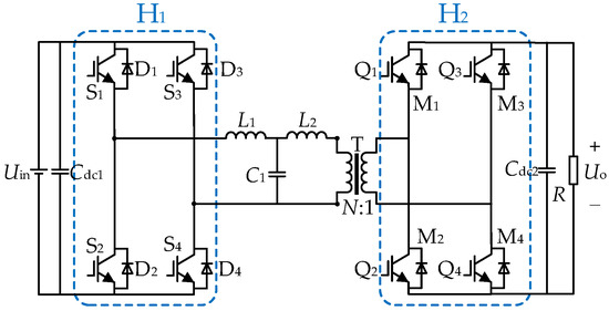
Figure 1.
Topology of the LCL-DAB DC-DC converters.
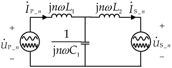
Figure 2.
Equivalent model of the LCL-DAB converter.
Taking forward power flow as an example, Figure 3 shows the main operating waveforms with the DPS modulation scheme, which shows that the duty ratios of all gate signals are 50%. The inner phase shift time d1T is the phase shift time between S1 and S4, or Q1 and Q4, corresponding to the time interval of zero voltage time of uP and uS. The outer phase shift time dT is defined as the time difference between the symmetry axis of uP and uS, and its polarity determines the direction of power flow. Since the time origin setting does not affect the conclusion of the following analysis, the origin of the time axis is set to the midpoint of the positive level of uS for convenience of derivation. Therefore, the time-domain expressions of uP and uS are
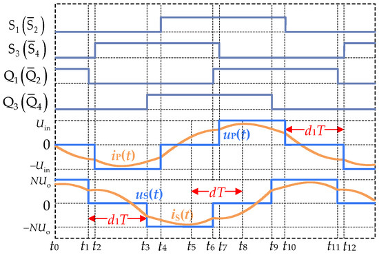
Figure 3.
Operating waveforms with DPS modulation scheme.
For a periodic signal f(x), it can be expanded into the form shown in (3), i.e., Fourier series.
where T is the period of f(x) and ω = 2π/T. Since the voltages and currents of the LCL resonant tank are periodic signals, the Fourier series expressions of them can be derived to (5) by substituting (1) and (2) into (4), respectively. Then, the phasor expression at each frequency can be expressed as (6).
where n = 1, 3, 5…. Here the resonant frequency is defined as , where fs is the switching frequency, and the resonant impedance is defined as . According to Figure 1, the voltage-current characteristic of the equivalent model is derived as
Substituting (6) into (7), the phasor expression of iP and iS can be deduced as
where k = NUo/Uin. Therefore, the time-domain expressions of iP and iS can be expressed by inverse derivation of (8), as
3. Modeling of the LCL-DAB Converter with DPS Modulation Scheme
Due to the switching action of the LCL-DAB converter, a severe nonlinear is presented in the system, which brings great difficulty to the system design process. Therefore, the small-signal analysis method is adopted to build the mathematical model of the LCL-DAB converter. The variables are approximated to the 0 and 1st order, which can avoid complex calculations and ensure high accuracy.
With DPS modulation scheme, the switching functions of H1 and H2 are defined respectively as
Therefore, based on the above analysis, the time-domain expression of uP and uS can be rewritten to
Since s1(t) and s2(t) are symmetrical in each half period, the DC terms of them are zero, and the real and imaginary parts of the 1st coefficient of their Fourier series expression are
Assuming that the current of inductors and the voltage of capacitors are state variables, so the continuous-time large-signal average equations are
It can be analyzed that all the DC terms of iP, iS and uC1 are equal to zero, and the ac terms of uo are zero. Then, a new matrix equation can be derived as
where
For the design and analysis of the system controller, the input-output small-signal model needs to be built, which is linear. Assuming that each of the state variables includes a large-signal state and a small-signal state, i.e., x = Δx + X, the expression of (17) can be rewritten. After extracting the small-signal state variables, the seventh-order small-signal model can be obtained, as
where
4. Direct Output Current Control Based on Virtual Voltage Compensation under No Backflow Power
In this section, the transmission power of LCL-DAB converters is derived. To ensure that the LCL-DAB converter operates without backflow power in a wide range and possesses a satisfactory transient response against input/output disturbances, a VDCC method of the LCL-DAB converter is proposed in this section. The power characteristic is first derived to estimate an appropriate value of d, enabling a wide range of no backflow power operation. Then, a VDCC method is proposed and analyzed to improve the transient performance.
4.1. Power Characteristic Analysis
For a two-port network with sinusoidal voltages and currents, the instantaneous power can be expressed as (26), where and are the active and reactive power, respectively. As shown in Figure 4, the first part of (26) is always positive while the second part is sometimes negative. Therefore, will be always positive if is eliminated, i.e., the backflow will be eliminated.
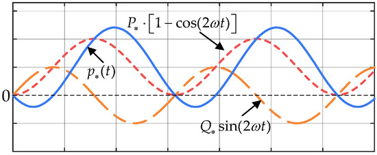
Figure 4.
The relationship between backflow power and reactive power.
If the parasitic parameters and losses of the converter are ignored, the output active power can be seen as the sum of the active power transferred by each harmonic, i.e.,
Similarly, the reactive power can be derived as
According to (28), it can be seen that Q1 = 0 when d = 0.25, which means that the backflow power corresponding to the fundamental component is eliminated. However, the reactive power of other harmonic components is not zero, meaning that the backflow power actually exists. To analyze the proportion of power generated by the harmonic components, the ratios of active and reactive generated by the harmonic components to the active power generated by the fundamental component are defined as the active power ratio YP and the reactive power ratio YQ, expressed as
Figure 5 shows the relationship between the active power ratio and phase shift ratios, indicating the active power ratio is closed 0 in most regions. Taking k = 1 as an example, Figure 6 shows the relationship between the reactive power ratio and phase shift ratios. Different from the active power ratio, the reactive power ratio changes significantly for different phased shift ratios. As a result, the transmission power expression can be expressed using the 1st harmonic approximation method, reduced from (27) to (31). However, 1st harmonic approximation method should not be utilized in the backflow elimination analysis, so it is necessary to adopt another method in the following calculation of design regions of no backflow power.
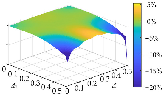
Figure 5.
Showing 3D plots of YP varying with d1 and d.
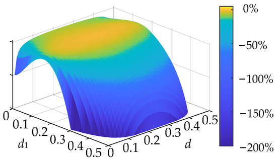
Figure 6.
Showing 3D plots of YQ varying with d1 and d.
The DC voltage gain of LCL-DAB converters is defined as GDC = Uo/Uin. With the resistive load R, the DC voltage gain can be calculated as
After removing the filter capacitor, the LCL-DAB converter can be regarded as a traditional DAB converter. Figure 7 shows the voltage gain curves of the LCL-DAB and the traditional DAB converter varying with phase shift ratios d1 and d. For both types of converters, the voltage gain GDC increases and then decreases with the increase in d and the curves are symmetric about the plane d = 0.25. Furthermore, GDC decreases with the increase in d1 and reaches zero when d1 = 0.5. It can be seen that the LCL-DAB converter can achieve higher voltage gain than the traditional DAB converter under the same inductance.
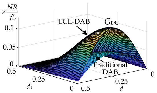
Figure 7.
Output voltage gain comparison for the two types of converters.
The above analysis indicates that it is inaccurate and infeasible to eliminate backflow power by eliminating reactive power using 1st harmonic approximation. Therefore, the exact design regions of no backflow power are presented and analyzed in the following section.
4.2. The Estimation of d
The waveforms of voltages and currents of the LCL-DAB converter are symmetrical in each half period, so the operating state only needs to be analyzed in half period. Taking the waveforms under no backflow power operation in Figure 3 as an example, the backflow power can be regarded as the negative part of the instantaneous power. Therefore, the consistent directions of uP and iP can be regarded as the criterion of no backflow power operation for H1, as expressed in (33) and (34). Similarly, the consistent directions of uS and iS can be regarded as the criterion of no backflow power operation for H2, as expressed in (35) and (36).
Substituting (9) into (33)–(36), the solutions of d1 and d of these constraints can be solved. Figure 8 shows the design boundaries of no backflow power for LCL-DAB converters with DPS modulation scheme, in which the regions surrounded by the curves are the design regions with different k. It also shows that the design regions for H1 expand with the increase in k, and the trend becomes unapparent with large values of k. On the contrary, the design regions for H2 shrink with the increase in k, and the trend becomes unapparent with small values of k. Notably, the design regions for H1 and H2 overlap when k = 1 (voltage matching), which means the same operating state of two bridges in the converter. Therefore, a reasonable k can be determined to avoid too narrow regions for H1 or H2 during the system design process.
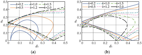
Figure 8.
Design regions of no backflow power operation with DPS modulation scheme: (a) for H1; (b) for H2.
The above analysis reveals that, for most values of k, the wide design ranges of d1 can be obtained when d is around 0.2, i.e., an appropriate value of d1 can ensure no backflow power operation in a wide range. Given that the output voltage gain is symmetric at d = 0.25, the preset modulation range of d should be determined for the first time according to the design acquirement. Moreover, other control objectives should be considered in the actual application, such as transmission power, output voltage, etc. Taking voltage gain as an example, for a fixed d, the uppercase form of it D denotes its steady state, so the maximal voltage gain can be expressed as (37), representing the voltage conversion ability. According to (37), the power conversion ability increases and then decreases with the increase in d and reaches the maximal value when D = 0.25. However, if only voltage gain is considered, the design region of no backflow operation could be nonexistent under a too tiny k for H1, or under a too large k for H2. Generally, the value of d should be weighed and determined according to the actual requirement.
4.3. Proposed VDCC Method
For the traditional output voltage control, the value of the feedforward compensation is constant, with the result that the PI controller will bear all the burden of adjusting the system for disturbances. In terms of transient response optimization against input voltage or load disturbances, a VDCC method is thus proposed, and its main principle is that the output current is directly controlled to meet the output current requirement.
Although the transmission power and voltage gain of the LCL-DAB converter are derived respectively as (31) and (32) based on the premise of lossless transmission, power losses cannot be ignored in the actual operation. Therefore, the input and output power are not equal, which means the calculated control variables are less accurate only according to the ideal equations. Moreover, the system parameters also can change varying to the operating conditions such as the inductance of the filter inductor, which also will result in the difference between ideal and required control variables. Therefore, a virtual voltage uov is introduced in the control loop to compensate for the difference, defined as
where ioref is the desired output current reference. Given that the resistance of the load is not constant, the instantaneous sampling values of the output voltage and current are utilized to calculate R, i.e.,
Substituting (39) into (38), the output current reference is derived as (40). Then, the instantaneous output current can be deduced, based on (31), as (41).
According to (40) and (41), the actual inner phase shift ratio d1* corresponding to the virtual output voltage can be derived, expressed as
where kf is a constant expressed as (43) and D is the estimated outer phase shift ratio. Based on the above analysis, Figure 9 shows the block diagram of the proposed VDCC method. The outer phase shift ratio is estimated based on Section 4.2 to ensure a wide range of no backflow operation, while the PI controller regulates the inner phase shift ratio mainly to make the output voltage follow the reference value. The input voltage uin, output voltage uo, and output current io need to be sampled once per cycle. The error between the sampled output voltage and the output voltage reference is calculated by the PI controller, and the output of the controller is set as the virtual voltage uov corresponding to the desired output current. The dynamic response improvement of the utilization of the virtual voltage has been verified in the traditional DAB converter [29,30]. Notably, the maximal value of the calculated direct output current should be limited according to the maximal output current of the converter, expressed as (44). Then, according to (42), the actual control variable d1* is calculated to improve the transient response against input voltage or load disturbances. Moreover, the introduction of the virtual voltage also can compensate for the difference between the calculated and the actual kf, which can be more flexible compared with the traditional constant feedforward compensation. Finally, the gate signals of the switches are generated according to d1* and D.
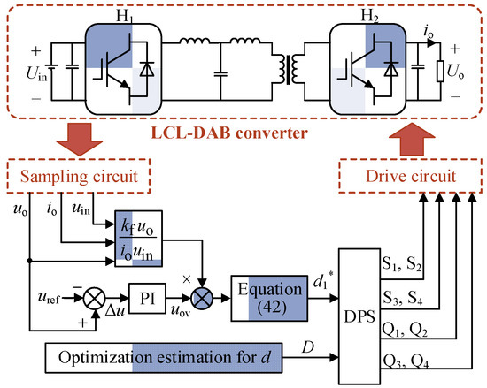
Figure 9.
Schematic diagram of the proposed VDCC method for fast transient response and no backflow power.
4.4. Disturbance Analysis of the VDCC Method
In the proposed VDCC method, the output voltage, the output current, and the input voltage have drastic influences on the system’s stability. Hence, the influences of output voltage, output current, and input voltage on the output voltage need to be discussed.
According to (42), the output voltage-to-inner phased shift transfer function can be expressed as
Similarly, the input voltage-to-inner phased shift and the output current-to-inner phased shift transfer functions can be derived, respectively as (46) and (47).
since the effects of the input voltage and the load disturbances are ultimately reflected in the output voltage. Based on (46), (47), and the small-signal model built in Section 4.3, the input voltage-to-output voltage and the output current-to-output voltage transfer functions can be derived, respectively as (48) and (49).
It can be summarized according to the above analysis that the small signals of the input voltage and the output current will affect the small signals of the output voltage due to the introduction of the compensation loop. Therefore, accurate sampled values of the control loop are needed to ensure control performance.
5. Simulation and Experimental Verification
5.1. Numerical Simulation Results
First of all, the wide range of no backflow power operation under an appropriate outer phase shift ratio is verified. For a fixed d which is set to 0.22, the value of d1 is changed to observe the open-loop results in the Matlab/Simulink model. The main simulation parameters are shown in Table 1 and the simulation waveforms are shown in Figure 10. According to the open-loop simulation results, the backflow power is basically eliminated for both bridges of the converter, for various values of k. Therefore, it can be summarized that an appropriate d ensures a wide range of no backflow power operation.

Table 1.
Main simulation parameters.
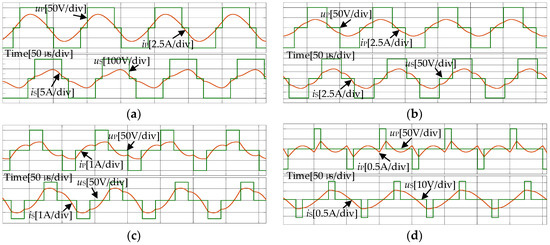
Figure 10.
The steady-state simulation waveforms: (a) d1 = 0.1; (b) d1 = 0.2; (c) d1 = 0.3; (d) d1 = 0.4.
5.2. Experimental Results
To verify the proposed VDCC method for fast transient response and no backflow power, the experimental prototype has been built, as shown in Figure 11. For experimental comparison, steady-state and transient experiments using the traditional constant compensation control method and the proposed VDCC method are conducted. The steady-state experiments are divided into four groups with the same output voltage Uo = 50 V, as shown in Table 2, i.e., Uin = 80 V, R = 50 Ω; Uin = 100 V, R = 50 Ω; Uin = 130 V, R = 50 Ω; Uin = 100 V, and R = 45.4 Ω.
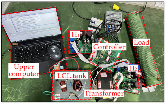
Figure 11.
Photo of the experimental platform.
Table 2.
Main experimental parameters.
Since the performance of backflow power elimination is mainly affected by the value of d, the traditional constant compensation control method and the proposed VDCC method have no obvious effect on the steady-state results of the backflow elimination. Therefore, for a unified comparison, the steady-state waveforms are obtained with the two control methods, as shown in Figure 12 and Figure 13. In Figure 12, d is set to 0.38, which is an inappropriate value of the outer phase shift ratio to achieve no backflow power operation according to the above analysis. It can be observed from Figure 12a to Figure 11d that the direction of currents and voltages sometimes are opposite at both sides of the LCL resonant tank, representing that the backflow is not eliminated in the input and output of the converter. In Figure 13, d is set to 0.22, which is an appropriate value of the outer phase shift ratio. According to these four figures, the currents are always reversed at zero voltage, so the backflow power is eliminated for both bridges of the converter. The elimination effectiveness of backflow power for an appropriate d matches the above simulation results, and, in addition, the current stress also decreases correspondingly.
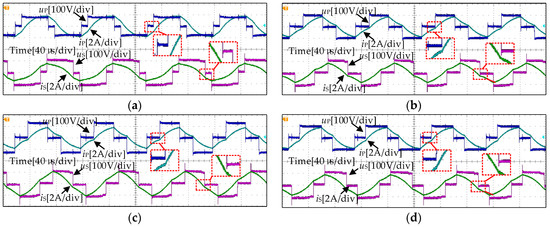
Figure 12.
The steady-state experimental waveforms with the traditional control method: (a) Uin = 80 V, R = 50 Ω; (b) Uin = 100 V, R = 50 Ω; (c) Uin = 130 V, R = 50 Ω; (d) Uin = 160 V, R = 45.4 Ω.
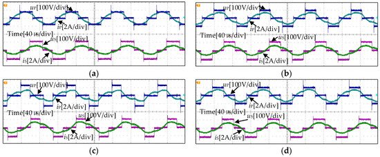
Figure 13.
The steady-state experimental waveforms with the proposed VDCC method: (a) Uin = 80 V, R = 50 Ω; (b) Uin = 100 V, R = 50 Ω; (c) Uin = 130 V, R = 50 Ω; (d) Uin = 160 V, R = 45.4 Ω.
To verify the transient response of the proposed VDCC method, the starting process, the transient response against input voltage disturbance, and the transient response against load disturbance are observed and compared with the traditional constant compensation control method.
Figure 14 shows the starting process of the two control methods, which indicates that the settling time with the proposed VDCC method is 121 ms, shorter than that with the traditional control method. Figure 15 and Figure 16 compare the transient response with two control methods under input voltage and load disturbances, and the steady-state waveforms before and after disturbances are the same as those in Figure 13b–d. As shown in Figure 15, when input voltage Uin is changed from 100 V to 130 V, the output voltage with the traditional constant compensation method first increases, and then is adjusted to the reference value while the output voltage with the proposed VDCC method remains stable. As shown in Figure 16, when the load R is changed from 50 Ω to 45.4 Ω, the overshoot of the output voltage with the proposed VDCC method is smaller than that with the traditional constant compensation method. Figure 15 and Figure 16 prove that the proposed VDCC method has superior transient performance against input voltage and load disturbances.
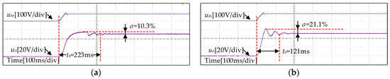
Figure 14.
Starting process experimental waveforms: (a) with the traditional constant compensation control method; (b) with the proposed VDCC method.
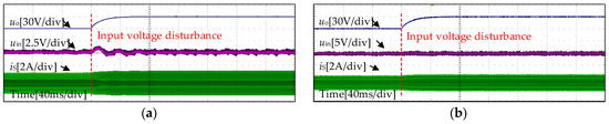
Figure 15.
Experimental waveforms when Uin is changed from 100 V to 130 V: (a) with the traditional constant compensation control method; (b) with the proposed VDCC method.
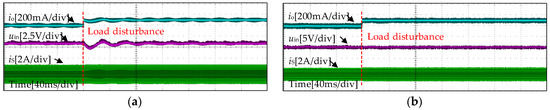
Figure 16.
Experimental waveforms when R is changed from 50 Ω to 45.4 Ω: (a) with the traditional constant compensation control method; (b) with the proposed VDCC method.
5.3. Experimental Efficiency Results Comparison
The efficiency of the LCL-DAB converter is mainly affected by the phase shift ratios, and the feedforward compensation type has no significant effect on it. Therefore, the experimental efficiency results are obtained with two values of d, corresponding to the above experiments. All experiments are implemented for a fixed 50 V output voltage and 50 Ω resistance of the load. As shown in Figure 17, the efficiency with the two outer phase shift ratios decreases with the increase in the input voltage, and the efficiency for d = 0.22 is higher than that for d = 0.38. Therefore, Figure 17 indicates the proposed VDCC method can improve the overall efficiency of the LCL-DAB converter in a wide range.
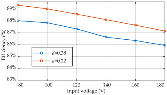
Figure 17.
Measured efficiency curves at different input voltages.
6. Conclusions
In this article, to eliminate the backflow power and improve the transient response against input voltage and load disturbances, a VDCC method for fast transient response and no backflow power is proposed. The voltage–current characteristic is first analyzed using the phasor method. Then the mathematical model of the LCL-DAB converter with DPS modulation scheme is built. On the basis of the derived power characteristics, the design regions of no backflow power are established, proving that an appropriate value of outer phase shift can ensure a wide range of no backflow power generation. Moreover, a VDCC method is proposed to improve the transient performance. Through the combination of the estimation of the outer phase shift and the virtual voltage compensation, the LCL-DAB with fast transient response can operate in a wide range of no backflow power, which can also compensate for the difference in the actual system parameters. Finally, the experimental prototype has verified that the proposed VDCC method with these system parameters can reduce the settling time of the starting process from 223 ms to 121 ms, and the system can remain at 0 ms settling time under the input voltage and load disturbances in a wide range of no backflow power operation.
Author Contributions
Conceptualization, M.L. and D.Y.; methodology, Z.L. and Z.W.; software, Y.Z.; validation, M.L., Z.L. and Y.Z.; formal analysis, Z.L. and M.L.; data curation, M.L.; writing—original draft preparation, M.L.; writing—review and editing, S.F. and C.Z.; supervision, D.Y.; project administration, D.Y. All authors have read and agreed to the published version of the manuscript.
Funding
This research was supported in part by the 2022 Postgraduate Research and Practice Innovation Program of Jiangsu Province under Grant KYCX22_2532 and the National Nature Science Foundation of China under Grant 51977208.
Institutional Review Board Statement
This study did not require ethical approval because it did not involve humans or animals.
Informed Consent Statement
Not applicable.
Data Availability Statement
Not applicable.
Conflicts of Interest
The authors declare no conflict of interest.
References
- Saponara, S.; Saletti, R.; Mihet-Popa, L. Hybrid Micro-Grids Exploiting Renewables Sources, Battery Energy Storages, and Bi-Directional Converters. Appl. Sci. 2019, 9, 4973. [Google Scholar] [CrossRef]
- Hou, X.; Sun, K.; Zhang, N.; Teng, F.; Zhang, X.; Green, T.C. Priority-Driven Self-Optimizing Power Control Scheme for Interlinking Converters of Hybrid AC/DC Microgrid Clusters in Decentralized Manner. IEEE Trans. Power Electron. 2022, 37, 5970–5983. [Google Scholar] [CrossRef]
- Kanathipan, K.; Lam, J. A high voltage gain isolated PV micro-converter with a single-voltage maximum power point tracking control loop for DC micro-grid systems. IEEE J. Emerg. Sel. Top. Ind. Electron. 2022, 3, 755–765. [Google Scholar] [CrossRef]
- Li, Y.; Zhang, H.; Liang, X.; Huang, B. Event-Triggered-Based Distributed Cooperative Energy Management for Multienergy Systems. IEEE Trans. Ind. Inf. 2019, 15, 2008–2022. [Google Scholar] [CrossRef]
- Liao, Y.-H.; Lin, Y. A Novel Bidirectional Wireless Power Transfer System for Mobile Power Application. Appl. Sci. 2019, 9, 3769. [Google Scholar] [CrossRef]
- Guo, L.; Zhang, S.; Li, X.; Li, Y.W.; Wang, C.; Feng, Y. Stability analysis and damping enhancement based on frequency-dependent virtual impedance for DC microgrids. IEEE J. Emerg. Sel. Top. Power Electron. 2017, 5, 338–350. [Google Scholar] [CrossRef]
- Li, P.; Wang, Y.; Liu, L.; Li, X.; Zuo, Z. Low frequency current-mode control for DC-DC boost converters with overshoot suppression. IEEE Trans. Circuits Syst. I Regul. Pap. 2022, 69, 4702–4713. [Google Scholar] [CrossRef]
- Li, Y.-C.; Chen, C.-J.; Tsai, C.-J. A Constant On-Time Buck Converter With Analog Time-Optimized On-Time Control. IEEE Trans. Power Electron. 2020, 35, 3754–3765. [Google Scholar] [CrossRef]
- Zhao, B.; Song, Q.; Liu, W.; Sun, Y. Overview of dual-active-bridge isolated bidirectional DC–DC converter for high-frequency-link power-conversion system. IEEE Trans. Power Electron. 2014, 29, 4091–4106. [Google Scholar] [CrossRef]
- Yan, Y.-H.; Cheng, H.-L.; Chan, S.-Y.; Chen, Y.-D.; Chang, Y.-N. Design of an Isolated Bidirectional Symmetric Resonant Converter. Appl. Sci. 2020, 10, 8144. [Google Scholar] [CrossRef]
- Li, X.; Bhat, A.K.S. Analysis and design of high-frequency isolated dual-bridge series resonant DC/DC converter. IEEE Trans. Power Electron. 2010, 25, 850–862. [Google Scholar]
- Wu, J.; Li, Y.; Sun, X.; Liu, F. A New Dual-Bridge Series Resonant DC–DC Converter With Dual Tank. IEEE Trans. Power Electron. 2018, 33, 3884–3897. [Google Scholar] [CrossRef]
- Jiang, T.; Zhang, J.; Wu, X.; Sheng, K.; Wang, Y. A bidirectional LLC resonant converter with automatic forward and backward mode transition. IEEE Trans. Power Electron. 2015, 30, 757–770. [Google Scholar] [CrossRef]
- Liao, Y.; Xu, G.; Peng, T.; Sun, Y.; Liu, D.; Yang, Y.; Su, M. An LLC-DAB Bidirectional DCX Converter with Wide Load Range 343 ZVS and Reduced Switch Count. IEEE Trans. Power Electr. 2022, 37, 2250–2263. [Google Scholar]
- Li, X.; Huang, J.; Ma, Y.; Wang, X.; Yang, J.; Wu, X. Unified Modeling, Analysis, and Design of Isolated Bidirectional CLLC Resonant DC–DC Converters. IEEE J. Emerg. Sel. Top. Power Electron. 2022, 10, 2305–2318. [Google Scholar] [CrossRef]
- Chen, W.; Rong, P.; Lu, Z. Snubberless Bidirectional DC–DC Converter With New CLLC Resonant Tank Featuring Minimized Switching Loss. IEEE Trans. Ind. Electron. 2010, 57, 3075–3086. [Google Scholar] [CrossRef]
- Jovcic, D.; Zhang, L. LCL DC/DC converter for DC grids. IEEE Trans. Power Deliv. 2013, 28, 2071–2079. [Google Scholar] [CrossRef]
- Thrimawithana, D.J.; Madawala, U.K.; Twiname, R.; Vilathgamuwa, D.M. A novel matrix converter based resonant dual active bridge for V2G applications. In Proceedings of the 2012 10th International Power & Energy Conference (IPEC), Ho Chi Minh City, Vietnam, 12–14 December 2012; pp. 503–508. [Google Scholar]
- Kan, J.; Xie, S.; Tang, Y.; Wu, Y. Voltage-fed dual active bridge bidirectional DC/DC converter with an immittance network. IEEE Trans. Power Electron. 2014, 29, 3582–3590. [Google Scholar] [CrossRef]
- Twiname, R.P.; Thrimawithana, D.J.; Madawala, U.K.; Baguley, C. A resonant bi-directional dc-dc converter. In Proceedings of the 2014 IEEE International Conference on Industrial Technology (ICIT), Busan, Republic of Korea, 26 February–1 March 2014; pp. 307–311. [Google Scholar]
- Twiname, R.P.; Thrimawithana, D.J.; Madawala, U.K.; Baguley, C.A. A new resonant bidirectional DC–DC converter topology. IEEE Trans. Power Electron. 2014, 29, 4733–4740. [Google Scholar] [CrossRef]
- Guo, Z.; Li, M. An optimized DPS control strategy for LCL resonant dual active bridge converter for wide voltage conversion ratio. IEEE J. Emerg. Sel. Top. Ind. Electron. 2021, 2, 501–512. [Google Scholar] [CrossRef]
- Guo, Z.; Li, M.; Han, X. Triple-phase shift modulation scheme of DAB converter with LCL resonant tank. IEEE Trans. Transp. Electrif. 2022, 8, 1734–1747. [Google Scholar] [CrossRef]
- Li, M.; Li, X.; Yu, D.; Leng, Y.; Zhang, C. Perturbation Observation Method Based Optimization Seeking Control of Soft-Switching and No Backflow Power for LCL Resonant-Type Dual Active Bridge DC-DC Converters. IEEE Trans. Ind. Electron. 2022. [Google Scholar] [CrossRef]
- Li, M.; Li, X.; He, C.; Wu, X. An optimized design method of phase-shift angle in DPS modulation scheme for LCL-type resonant DAB DC-DC converters. In Proceedings of the 2019 22nd International Conference on Electrical Machines and Systems (ICEMS), Harbin, China, 11–14 August 2019; pp. 1–6. [Google Scholar]
- Saha, T.; Bagchi, A.C.; Zane, R. Time-domain analysis and ZVS assistance design for a DAB LCL-T resonant converter in underwater DC current distribution network. In Proceedings of the 2020 IEEE 21st Workshop Control Model. Power Electronics (COMPEL), Aalborg, Denmark, 9–12 November 2020; pp. 1–7. [Google Scholar]
- Saha, T.; Bagchi, A.C.; Zane, R.A. Analysis and design of an LCL–T resonant DC–DC converter for underwater power supply. IEEE Trans. Power Electron. 2021, 36, 6725–6737. [Google Scholar] [CrossRef]
- Li, M.; Guo, Z. Model predictive control of LCL resonant dual active bridge converter. In Proceedings of the 2021 IEEE 1st International Power Electronics and Application Symposium (PEAS), Shanghai, China, 12–15 November 2021; pp. 1–6. [Google Scholar]
- Song, W.; Hou, N.; Wu, M. Virtual direct power control Scheme of dual active bridge DC–DC converters for fast dynamic response. IEEE Trans. Power Electron. 2018, 33, 1750–1759. [Google Scholar] [CrossRef]
- Hou, N.; Ding, L.; Gunawardena, P.; Zhang, Y.; Li, Y.W. A Comprehensive Comparison of Two Fast-Dynamic Control Structures for the DAB DC–DC Converter. IEEE Trans. Power Electron. 2022, 37, 6488–6500. [Google Scholar] [CrossRef]
Disclaimer/Publisher’s Note: The statements, opinions and data contained in all publications are solely those of the individual author(s) and contributor(s) and not of MDPI and/or the editor(s). MDPI and/or the editor(s) disclaim responsibility for any injury to people or property resulting from any ideas, methods, instructions or products referred to in the content. |
© 2023 by the authors. Licensee MDPI, Basel, Switzerland. This article is an open access article distributed under the terms and conditions of the Creative Commons Attribution (CC BY) license (https://creativecommons.org/licenses/by/4.0/).