Featured Application
The precise relationship between material thickness and material properties will guide the application of layered black phosphorus materials.
Abstract
As a two-dimensional (2D) semiconductor material with excellent optoelectronic properties, black phosphorus (BP) has attracted widespread attention. It was found that the energy band structure of BP crystal changes with its thickness if BP is thin. To explore the accurate effects of the BP thicknesses on devices, BP-FETs with different BP thickness (50 nm, 40 nm, 30 nm, 20 nm, and 6 nm) as the channel material were fabricated by mechanical exfoliation technique. The output characteristics and transfer characteristics of the BP-FETs were analyzed in detail. The source–drain current (Ids) of devices is directly related to the BP thickness. The larger the BP thickness, the larger the Ids obtained under the same gate voltage modulation, but the electric field modulation effect decreases. Especially, the correlation between Ids and BP thickness can be described by a semi-empirical formula, which predicts that only when the BP thickness is less than 21.7 nm, the band structure of BP will be significantly affected by the thickness. The mobility of the carrier increases with the increasing of the BP thickness; for BP thickness of 6 nm, 20 nm, 30 nm, 40 nm, and 50 nm, the mobility is about 52.5 cm2/Vs, 187.5 cm2/Vs, 214.4 cm2/Vs, 252.5 cm2/Vs, and 336.4 cm2/Vs. Finally, the 50 nm BP in FET was etched to 30 nm using plasma etching technology to further verify the above experimental results. It also confirmed that plasma etching methods tend to introduce structural damage and impurity elements, which in turn has an impact on the output characteristics of the device.
1. Introduction
Graphene (G) has an absolute advantage in the preparation of high-frequency devices due to its ultra-high electron mobility, but the intrinsic graphene has no band gap, which limits its application in logic devices [1,2]. The transition metal chalcogenides (TMDs) represented by molybdenum disulfide (MoS2) make up for the defect of zero band gap of graphene. The field-effect transistors (FETs) prepared by them show superior switching modulation characteristics, so they have great advantages in low-power devices [3,4,5,6,7]. However, the intrinsic carrier mobility of two-dimensional TMDs is usually low, much lower than the electron mobility in crystalline silicon [8,9], which greatly limits their application in semiconductor electronic devices. Of course, there are more and more methods to improve the carrier mobility of TMDs.
As another important discovery after graphene and transition metal sulfide, black phosphorus (BP), as the only other known monotypic van der Waals crystal, has broad application prospects in nano optoelectronic devices [10,11,12,13,14,15,16,17,18,19]. In 2014, a FET with nanometer thickness two-dimensional BP as channel material was successfully prepared by the research group of Zhang et al. [20]. The test results show that the on/off current ratio of the BP transistor could reach 105 when the thickness of the two-dimensional BP film is less than 7.5 nm, and the highest electron mobility maybe reaches ~1000 cm2/Vs when the thickness of BP film is greater than 10 nm, which is somewhat better than that of molybdenum disulfide (~200 cm2/Vs). BP has become another important member of the two-dimensional nanomaterial family following graphene and molybdenum disulfide [21,22,23,24,25]. In the research of BP materials and their devices, the band structure of BP crystals was found to change with the thickness of the material itself, i.e., the band gap decreases with increasing thickness [22,26]. Saptarshi et al. derived the band gap of BP samples with different layers (less than 30 layers) [27] by computer theoretical simulation. By measuring the transport characteristics of BP FETs with different thicknesses, they confirmed this conclusion experimentally. Liang et al. report the evolution of the band gap calculated by different methods from 1 layer to ∞ layers, and show the sheet conductivity as a function of gate voltage for devices with different thicknesses (10 nm, 8 nm, and 5 nm) [22]. However, for BP thickness larger than 30 layers or higher (over 20 nm), the precise effect of material thickness on device characteristics or functional relationship between electrical characteristics (output characteristics, transfer characteristics, mobility, etc.) and thickness have not been systematically studied.
Here, the effects of BP materials with thicknesses ranging from ~10 to ~100 layers on the transport properties of BP-FETs were precisely investigated. Five BP-FET devices with different BP thicknesses (~50 nm, ~40 nm, ~30 nm, ~20 nm, and ~6 nm) were prepared by mechanical exfoliation technology, and their electrical properties were tested in detail. The influence of BP material thickness on device output and transfer characteristics were systematically analyzed. Using plasma etching technology to etch the material thickness of 50 nm to 30 nm again confirmed the effect of thickness on device performance.
2. Materials and Methods
The preparation of the device was based on the mechanical exfoliation method of thin adhesive tape described in previous reports in detail [28]. The thin layer of BP is obtained from the BP crystal, and the BP sheet is exfoliated to the SiO2/Si (285 nm SiO2/highly doped n-type Si) substrate by tape. Through the difference of color and transparency under the microscope, the material with light color and high transparency is selected as the experimental material. The silicon substrate before use is rinsed with deionized water and dried with nitrogen gas gun. Standard electron beam lithography (EBL) and metal evaporation are used to prepare electrodes. The two-dimensional material sample was first transferred to a silicon substrate with alignment marks. The sample is placed into a scanning electron microscope (SEM, model FEIF50), and then it is positioned using the alignment markers, and an electrode is written on the sample using a pattern generator. The sample surface is spin-coated with 500 nm thickness of electron beam photoresist PMMA and baked on a hot plate for 90 s (temperature of 180 °C). Then, the sample is put into the electron beam exposure system and the drawn electrode pattern is exposed. Then, the samples are developed in the developing solution (MIBK:IPA = 1:3) for 1 min, followed by washing with IPA for 1 min and blowing dry with a nitrogen gun. The sample is then placed on an electron beam evaporation table to evaporate the metal electrode (e.g., Ti/Au). After the vaporization, the sample is immersed in acetone, and the PMMA and the metal on the surface are removed by the lift-off process, cleaned in IPA for 5 min, and dried with a nitrogen gun to complete the electrode fabrication. The device preparation process is shown in Figure 1a.
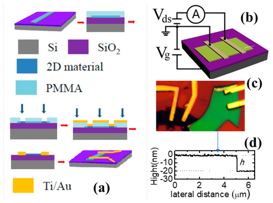
Figure 1.
(a) Schematic diagram of device preparation process, (b) device schematic diagram, (c) the real device diagram, the BP thickness on the right side is about 20 nm, (d) its thickness measurement of one material by atomic force microscope.
The schematic diagram of device is shown in Figure 1b. One prepared device is shown in Figure 1c, and the ratio of the length to width of channel of the device is kept approximately at 1.2 during EBL. The electrode part of the device is a chromium/gold electrode (10 nm/20 nm). The electrode materials, electrode thickness, substrate, substrate insulation layer thickness, device preparation method, device preparation conditions, the time between device preparation and test, and the device test conditions used by the five devices are identical, and the devices are not subject to any treatment such as annealing, lighting, etc.
The electrical characteristics of the device are measured through B1500A Semiconductor Device Parameter Analyzer configured on the Cascade DC probe platform. Optical microscopy and atomic force microscopy (AFM) were used to find layer samples and to determine their thickness. All tests were performed at room temperature. Because all devices have the same process and all materials with thickness above 20 nm have a similar dark green color, Figure 1 only shows the preparation process and thickness measurement process of one device.
3. Results
Figure 2a shows the output characteristics (Ids-Vds) of about 50 nm, 40 nm, 30 nm, and 20 nm BP FET devices. The source drain voltage scanning range is from −100 mV to 100 mV, and the gate voltage (Vg) is 0 V. Figure 2b shows the Ids-Vds characteristics of about 6 nm BP FET, but the Vds scanning range is from −50 mV to 50 mV. This range is mainly due to the thin material and the need to prevent the device from being damaged. The good linear relationship between Ids and Vds (all fit lines are very good straight lines) proves that a good contact is formed between the BP and the electrode. It can be clearly seen that at a fixed Vds, the value of Ids increases gradually with the increase of the material thickness. Namely, the greater the thickness of the material, the greater the Ids. However, the Ids changes only a few times for a thickness changing from 20 nm to 50 nm, but from 6 nm to 20 nm, the Ids does change by several orders of magnitude.
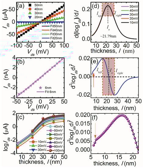
Figure 2.
(a) Output characteristics (Ids-Vds) of BP FET devices with thickness of 50 nm, 40 nm, 30 nm, and 20 nm, and (b) of 6 nm at Vg = 0 V, and their fitting curves; (c) the dependence of logIds on thickness at different Vds, and their fitting curves. In (a–c) the scattered geometry represents the experimental data points and the solid line is the fitted curves. (d) First order differential curve of logIds vs. l, all curves are completely coincident; (e) the second differential curve of logIds vs. l of 10 mV. The left side of the shaded part corresponds to lleft and the right side corresponds to lright, which are approximately 16.3 nm and 26.7 nm, respectively. (f) is an enlarged graph of the curve in (e) at small thickness.
Figure 2c shows the exact change rule of Ids with BP material thickness under different Vds. Interestingly, the laws of several curves are completely consistent, so it is certain that there is a certain relationship between the Ids of the BP FET device and the BP thickness. Using 1stOpt (First Optimization, 7D-Soft High Technology Inc.), a simulation software that can easily fit the experimental data, we fitted the experimental data (logIds) shown in Figure 2c with Boltzmann model, and the fitted curves can be obtained. The change rule of logIds and BP thickness l can be described by the following semi empirical formula given by software,
where A, B, lo, and C are fitting coefficients, their values have very weak changes with BP thickness, as shown in Table 1. The fitting results show that the experimental data of logIds-l in Figure 2c fitted by Formula (1) and the coefficients in Table 1 give an Radj2 of over 0.998, which reflects a very perfect fit (usually Radj2 = 1 indicates complete agreement and Radj2 = 0 indicates complete failure) [29]. That is, Equation (1) can completely describe logIds-l. As the material thickness increases, A and C slightly increase, while B and lo slightly decrease. However, only the coefficient A exhibits a pattern of increasing with the thickness of the material, for B, C, and lo, the influence of thickness can be almost ignored when the BP thickness is greater than about 20 nm. For example, when BP thickness from 20 nm to 50 nm, B simply fluctuates between −3.990 and −3.989; lo also fluctuates within a range (shown in Table 1 and Figure 3b,c). Next, we analyze the impact of l on Ids in detail.

Table 1.
Fitting parameters.
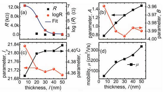
Figure 3.
(a) The change of device total resistance with material thickness, and its fitting curve of logR vs. l; (b–d) are the change of fitting coefficients and the carrier mobility with the material thickness.
Figure 2d shows that the kink point of the slope of the fitting curve (the maximum value of the first order differential) appears near lo. The value of lo is 21.7 nm. Above lo, the slope of the curve starts to decrease slowly, but gradually becomes faster. When l reaches a certain value lright, the speed of the slope decreases reaches the fastest. Thereafter, the speed of decrease gradually becomes slower. If l continues to increase, when it approaches 50 nm, the speed of the slope decrease of the curve reaches almost 0, and then the fitting curve gradually flattens, which means that the degree of influence of thickness on device characteristics can be ignored. Figure 2e again proves the above conclusion that when the l is greater than 21.7 nm, the minimum value of the slope of the dlogIds/dl-l occurs at the BP thickness of 26.7 nm (negative, but its absolute value is the maximum). Namely, lright is 26.7 nm. That is, when the thickness is greater than 26.7 nm, the effect of thickness on device characteristics gradually starts to become less pronounced.
Below lo, although we did not measure the transport characteristics of FETs with BP thickness up to 6 nm, it seems possible to predict from Figure 2d that when the channel material thickness is less than lleft (kink point), the effect of l on Ids seems to become progressively less pronounced as the l decreases. The region where the degree of the effect of thickness on Ids is most pronounced should be around lleft (16.3 nm) because the change of slope of the curve is the fastest near lleft, as shown in Figure 2e. From 6 nm to 16.3 nm, the speed of the slope increse of logIds-l is gradually increasing with the increase of the thickness, reaching the maximum at 16.3 nm, after which it gradually becomes smaller and is 0 at 21.7 nm.
The extent of the effect of BP thickness on device performance at different thickness ranges can be obtained from Figure 2e. The speed of slope varies from the maximum (at lleft) to the minimum (at lright), but the thickness spans only 10.4 nm. From 6 nm to 16.3 nm, the speed varies from a non-zero value to a maximum value, although the span of l is only 10.3 nm, but the span of speed is only half of the interval of 16.3 nm to 26.7 nm. From 26.7 nm to 50 nm, speed varies from the minimum to 0, where l spans 23.3 nm and speed spans half of the interval 16.3 nm to 26.7 nm. Alternatively, when the thickness of the BP material is between 16.3 and 26.7 nm, the BP thickness should have a significant effect on device performance, even greater than the effect of thickness on device characteristics when the thickness is between 20 nm and 6 nm (or 26.7–50 nm), although the thickness of the material also has a significant effect on device characteristics when the thickness of the material is thin (20 nm to 6 nm). Of course, Figure 2e shows more clearly that when the thickness reaches or exceeds 50 nm, the l has almost no effect on Ids. In addition, when the thickness is between 6 nm and 7 nm, it seems that the degree of influence of thin layer thickness on the output characteristics of the device is changed more significantly, shown in Figure 2f. According to previous literature reports [30,31], we believe that other factors may be involved in influencing the performance of device with thin BP thickness. By linear fitting Figure 2a,b, from their slopes the total resistance of devices with BP thickness of about 50 nm, 40 nm, and 30 nm are extracted as about 1.52 kΩ, 2.18 kΩ, and 5.4 kΩ, respectively. It seems to decrease linearly with the increase of thickness. However, the resistance of about 20 nm and 6 nm BP devices are nonlinear increased to 420.2 kΩ and 12,733.9 kΩ. That is, when the device material thickness changes from ~30 nm to ~20 nm, the resistance of the device increases by a factor of nearly 78; while the material thickness changes from ~20 nm to ~6 nm thickness, its resistance increases by a factor of 30. This corroborates the results in Figure 2 that the thickness of the BP material is more influential on the device performance when the thickness range is between ~16.3 nm and ~26.7 nm. The specific relationship between the resistance of devices and the thickness of channel materials is shown in Figure 3a. This super nonlinearity may be due to the fact that when the material thickness is reduced to a certain value, the band gap of the material increases, resulting in a sudden increase in resistance. In addition, using 1stOpt we fitted the logR vs. BP thickness l in Figure 3a, and found that the function of the relationship between fitted logR and l is also the above Formula (1), and the fitting parameters A, B, C, and lo are 3.22190, 3.987341, 4.34556, and 21.79109, respectively. The coefficients are almost identical to those in Table 1, except for the A coefficient in Equation (1). However, after a closer look at Equation (1), it is found that the coefficient A is a constant determined independent of thickness. Therefore, both logIds and logR vs. l should be mainly determined by the second term on the right side of Equation (1), so the Equation (1) can also describe the relationship between logR and l. From this experiment, we can predict that when the band gap starts to change with the thickness, the corresponding value of thickness should be lo, ~21.7 nm. Namely, when the BP thickness is less than 21.7 nm, the energy band of BP material will increase significantly with the thickness thinning, and when the BP thickness is greater than it, the modulation relationship between the energy band of BP material and the thickness will gradually weaken. This conclusion is similar to that of Figure 2d. The exact relationship of the four fitted coefficients in Table 1 with thickness is shown in Figure 3b and c, it seems to confirm that only the A coefficient is determined with thickness, while the other coefficients vary little or not at large material thicknesses (for ~20 nm).
Figure 4 shows the transfer characteristic (Ids-Vg) curves of BP FET devices with thickness of about 50 nm, 40 nm, 30 nm, 20 nm, and 6 nm, respectively. The Vds is 100 mV. It is obvious that the larger the thickness, the less the applied electric field can regulate the device. For the device with BP of ~50 nm, the current only changes from a maximum value of 75 mA to a minimum value of 60 mA at −40 V to 40 V electric control voltage, a change of 1.25 times. The same is true for a 40 nm thick device. This weak dependence on the gate voltage (Vgs) due to strong Thomas–Fermi charge screening in thick BP flakes. In addition, if the FET device has a thick BP material (greater than 20 nm), no Ioff is seen in the measured voltage range, namely, the device material exhibits a very clear p-type because no minimum value of current (flatband condition voltage, VFB) is seen [32]. In the inset of Figure 4b, we found that the dominant carrier type in BP will change from naturally p-type to n-doping in FET with thinner BP flakes at VFB. The VFB are about −4.5 V and 2.2 V for FET with the BP thicknesses of 6 nm and 20 nm, respectively. It seems that for natural p-type BP materials, the greater the thickness, the greater the VFB, i.e., the greater the Vg required to shift the polar type of the material. Furthermore, the Ioff was observed in devices with 6 nm and 20 nm thickness material, the Ion/Ioff is ~103.
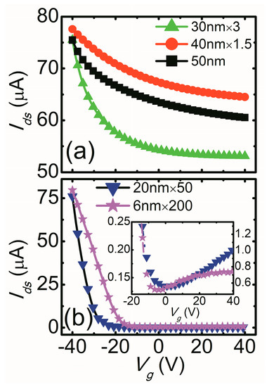
Figure 4.
(a,b) are the transfer characteristic curves of BP-FET devices with thickness of 50 nm, 40 nm, 30 nm, 20 nm, and 6 nm, respectively. Vds is set to 100 mV. Except for FET with 50 nm BP, the Ids of FET with other thicknesses have been amplified by 1.5 times, 3 times, 50 times, and 200 times, respectively, for FETs with thickness of 40 nm, 30 nm, 20 nm, and 6 nm. The inset of (b) is a magnified view of the Vg between −20 V and 40 V.
At different gate voltages (Vg) the Ids-Vds curves of BP FET devices with about 50 nm, 40 nm, 30 nm 20 nm, and 6 nm BP are shown in Figure 5, where the source drain voltage (Vds) scanning range is from −100 mV to 100 mV. It can be seen that the Ids of the BP-FET device is directly related to the thickness of the material. The thicker the material is, the greater the source drain current under the same Vg. However, the thicker the material is, the weaker the modulation effect of the electric field will be, which can be seen from Figure 5a, at different Vg, several curves basically overlap. In addition, when the thickness of the material is reduced to about 20 nm, under the Vg modulation of 40 V, the source leakage current has been reduced by 5000 times compared to BP-FET with the 30 nm material.
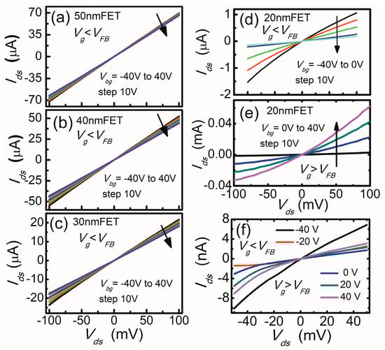
Figure 5.
(a–f) The Ids-Vds curves at different Vg, BP thickness of FET are 50 nm, 40 nm, 30 nm, 20 nm, and 6 nm, respectively. The Vg is from −40 V to 40 V.
However, the modulation effect of the electric field is enhanced, and the on/off current ratio (the ratio of the on-state current to the off-state current) of the device reaches ~103. In addition, from the transfer characteristic curve, it can be seen that when the negative gate voltage is greater, its conductivity is better, so majority carriers are holes. When the BP thickness is about 20 nm and 6 nm, the transfer characteristic curve of the device indicates that the type of carriers involved in conducting in the BP crystal has shown a certain bipolar type (as shown in the Figure 4b), which is similar to the BP FET of the thin layer materials (below 10 nm) [8]. From the inset of Figure 4b, the thinner the material is, the smaller the modulation voltage required for the carrier polar transition. According to the transfer characteristic curve of FET, the carrier mobility can be calculated according to the following formula [31].
where L/W is the ratio of length and width of the device channel. In our prepared BP-FET, the ratio is 1.2, Ci = ɛoɛi/d is the capacitance per unit area, ɛo = 8.854 × 10⁻¹² fm−1 is the dielectric constant in vacuum, ɛi = 3.9 is the relative dielectric constant of silicon dioxide, and d is the thickness of the insulating layer, that is, the thickness of silicon dioxide. It is 285 nm. We can calculate that the values of the device mobility with BP thickness of about 50 nm, 40 nm, 30 nm, 20 nm, and 6 nm are about 336.4 cm2/Vs, 252.5 cm2/Vs, 214.4 cm2/Vs, 187.5 cm2/Vs, and 52.5 cm2/Vs. The exact relationship between mobility and BP thickness is shown in Figure 3d. The carrier mobility increases with the increase of material thickness, and from 20 nm to 50 nm, it can be approximately regarded as proportional to the thickness. However, the most significant increase in device mobility was observed when the BP thickness is increased from 6 nm to 20 nm. The reason for the rapid increase can also be attributed to the fact that when the BP thickness is less than 21.7 nm, the band gap of BP is modulated by the thickness, thus affecting the mobility.
In order to verify the above conclusions, we used plasma etching technology to etch the BP device with a thickness of 50 nm. Under specific power and current, after controlling the etching rate for 30 s, a BP-FET with a thickness of about 30 nm was obtained. Figure 6a shows its output characteristics. In the three Ids-Vg curves, the source drain voltage scanning range is from −100 mV to 100 mV, and the gate voltages are set at 30 V, 0 V, and −30 V, respectively. Figure 6b shows the transfer characteristics. The Vg scanning range is from −30 V to 30 V, and the source drain voltage is set at 100 mV. Compared with the output characteristics of the BP FET in Figure 5c, the current of the etched BP FET is close to that of the 30 nm BP FET and greatly reduced compared with that of the 50 nm BP FET, which confirms that in the electrical characteristics of the BP FET is directly related to the BP thickness. Under the same Vg, the greater the BP thickness, the greater the source drain current. However, the I-V curve in Figure 6a has kink points. The reason for this phenomenon is that the plasma etching method often introduces different levels of structural damage and impurity elements, causing damage to the lattice structure of the sample materials. From the transfer characteristics in Figure 6b, it can be concluded that the thickness of the material will affect the modulation of the electric field. By comparing the transfer characteristic curve of the BP FET with 30 nm BP in Figure 4a, it can be seen that the electric field modulation effect is more obvious in the device after plasma etching. Since the device after plasma etching has better conductivity when the negative gate voltage is higher, most carriers are holes, which is consistent with the above conclusion.
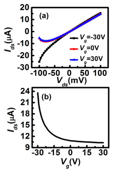
Figure 6.
Transport characteristics of a FET with 30 nm BP etched from 50 nm, (a) the output characteristic curve, (b) the transfer characteristic curve.
4. Discussion
In this paper, FETs with five different BP thicknesses as channel material were prepared by dry transfer technology. Material thickness spans from 6 nm to 50 nm, corresponding to a layer count of approximately 10 to 100 layers. The relationship between the thickness of the channel material of the FET and the electrical properties of the FETs were systematically investigated.
4.1. Effect of the l on Ids
By studying the electrical characteristics of these devices, we can conclude that the Ids of BP-FET was directly related to the l of the BP material under the same test environment. The greater the l is, the greater the Ids under the same gate voltage (Vg) regulation is, but the modulation effect of the electric field will weaken with the increase of the l. When Vg = 0, under different but fixed Vgs, there is a very good rule between Ids and l, which can be expressed by a very accurate empirical formula. An approximate thickness lo (21.7 nm) can be deduced from this formula, at this point, the slope of the logIds-l takes the maximum value. Namely, the influence of l on logIds is obvious in the vicinity of lo. The thickness region with the most significant effect on the Ids of device is between 16.7 nm and 27.3 nm. Then, if BP thickness is less than 16.7 nm, the influence of thickness on device characteristics will increase as the l increases; but if BP thickness is greater than 27.3 nm, the influence of thickness on characteristics will be weak with the increasing l. When the thickness reaches or exceeds 50 nm, the l has almost no effect on logIds.
4.2. Effect of the l on R and μ
The total resistance of the device decreases with the increase of the material thickness, but it shows a nonlinear change with the thickness. The relationship between resistance and thickness still meets the above semi empirical formula. The carrier mobility increases with the increase of the material thickness. This is mainly because the gm (the peak transconductance extracted from the linear scale of transfer behaviors) increases with thickness. Although the relationship between mobility and thickness does not meet the above formula, when BP changes from 6 nm to 20 nm, its value changes much more than when BP changes from 20 nm to 50 nm. This is mainly because when the thickness of the material is less than 21.7 nm, the influence of the thickness of the material on the material band gap is significantly enhanced. Therefore, as the thickness of the BP material decreases, the band gap gradually increases, and the resistance increases significantly.
After the device is etched by plasma etching technology, the above conclusions are verified, and the modulation effect of gate voltage on current is more obvious in the plasma etched FET device. In addition, experiments have shown that the plasma etching method often introduces different levels of structural damage and impurity elements, causing damage to the lattice structure of the sample materials, which in turn has an impact on the output characteristics of the device.
5. Conclusions
The experimental results do show that the thickness of the FET channel material does have a large effect on the electrical transport characteristics of the device, and the effect is greater when the material is thinner, and this result is basically consistent with previous reports. However, we also have to admit that the results obtained in this experiment are different from those previously reported. It is generally believed that the relationship between BP thickness and BP energy band is such that the significant broadening of the energy band of the material with decreasing thickness occurs only when the thickness is less than ~4 nm, and this variation relationship is nonlinear, i.e., when the material thickness is less than ~4 nm, the smaller the thickness the faster the increase of the energy band width. However, the experimental results show that the material thickness is near 16 nm, the change of thickness began to have a large impact on the device performance, and the impact was the most significant at this time; after that, as the material becomes thinner, device characteristics also change, but not an obvious non-linear change. This also confirmed that the material band gap, which is significantly affected by thickness in thin BP, is only one factor affecting the performance of the FET device. Stability and contact interface between BP and electrode are also essential consideration in the influence on the properties of thin-layer materials and their devices. Generally, the thinner the BP, the stronger the effect its stability may have on the performance of the device, in particular in the presence of both oxygen and water [30]. Therefore, to prepare 2D BP-FET devices with excellent performance for future nanoelectronic and optoelectronic applications, one needs to consider the combined effects of material thickness, environment, device structure, contact electrodes, and other factors.
Author Contributions
Conceptualization, L.F.; methodology, L.F. and K.L.; data curation, K.L. and M.W.; writing—original draft preparation, K.L. and M.W.; writing—review and editing, L.F.; supervision, L.F.; project administration, L.F.; funding acquisition, L.F. All authors have read and agreed to the published version of the manuscript.
Funding
National Natural Science Foundation of China, grant number 12274319 and 61804010, and by Natural Science Foundation of Tianjin City grant 17JCYBJC16200.
Data Availability Statement
Not applicable.
Conflicts of Interest
The authors declare no conflict of interest.
References
- Lou, D.; Chen, S.; Langrud, S.; Razzaq, A.A.; Mao, M.Y.; Younes, H.; Xing, W.B.; Lin, T.; Hong, H.P. Scalable Fabrication of Si-Graphene Composite as Anode for Li-ion Batteries. Appl. Sci. 2022, 12, 10926. [Google Scholar] [CrossRef]
- Schwierz, F. Graphene Transistors. Nat. Nanotech. 2010, 5, 487–496. [Google Scholar] [CrossRef] [PubMed]
- Han, M.Y.; Ozyilmaz, B.; Zhang, Y.B.; Kim, P. Energy band-gap en-gineering of graphene nanoribbons. Phys. Rev. Lett. 2007, 98, 206805. [Google Scholar] [CrossRef] [PubMed]
- Wang, Q.S.; Zheng, J.C.; He, Y.; Cao, J.; Liu, X.; Wang, M.Y.; Ma, J.C.; Lai, J.W.; Lu, H.; Jia, S.; et al. Robust edge photocurrent response on layered type II Weyl semimetal WTe2. Nat. Commun. 2019, 10, 5736. [Google Scholar] [CrossRef] [PubMed]
- Fei, Z.Y.; Zhao, W.; Palomaki, T.A.; Sun, B.S.; Miller, M.K.; Zhao, Z.Y.; Yan, J.Q.; Xu, X.D.; Cobden, D.H. Ferroelectric switching of a two-dimensional metal. Nature 2018, 560, 336–339. [Google Scholar] [CrossRef]
- Xu, S.Y.; Ma, Q.; Shen, H.T.; Fatemi, V.; Wu, S.F.; Chang, T.R.; Chang, G.Q.; Valdivia, A.M.M.; Chan, C.K.; Gibson, Q.D.; et al. Electrically switchable Berry curvature dipole in the monolayer topological insulator WTe2. Nat. Phys. 2018, 14, 900–906. [Google Scholar] [CrossRef]
- Wu, M.K.; Liu, P.; Xin, B.J.; Li, L.Y.; Dong, H.; Cheng, Y.H.; Wang, W.C.; Lu, F.; Cho, K.; Wang, W.H.; et al. Improved carrier doping strategy of monolayer MoS2 through two-dimensional solid electrolyteof YBr3. Appl. Phys. Lett. 2019, 114, 171601. [Google Scholar] [CrossRef]
- Radisavljevic, B.; Radenovic, A.; Brivio, J.; Giacometti, V.; Kis, A. Single-Layer MoS2 Transistors. Nat. Nanotechnol. 2011, 6, 147–150. [Google Scholar] [CrossRef]
- Pradhan, N.R.; Rhodes, D.; Zhang, Q.; Talapatra, S.; Terrones, M.; Ajayan, P.; Balicas, L. Intrinsic carrier mobility of multi-layered MoS2 field-effect transistors on SiO2. Appl. Phys. Lett. 2013, 102, 699. [Google Scholar] [CrossRef]
- Lu, S.B.; Miao, L.L.; Guo, Z.N.; Gou, X. Broadband nonlinear opti-cal response in multi-layer black phosphorus: An emerging infrared and mid-infrared optical material. Opt. Express 2015, 23, 11183–11194. [Google Scholar] [CrossRef]
- Zhang, S.; Yang, J.; Xu, R.J.; Wang, F.; Li, W.F.; Muhammad, G.; Zhang, Y.W.; Yu, Z.F.; Zhang, G.; Qin, Q.H.; et al. Extraordinary photolumines-cence and strong temperature/angle-dependent raman re-sponses in few-layer phosphorene. ACS Nano 2014, 8, 9590–9596. [Google Scholar] [CrossRef] [PubMed]
- Rodin, A.S.; Carvalho, A.; Castro, N.A.H. Strain-induced gap modification in black phosphorus. Phys. Rev. Lett. 2014, 112, 176801. [Google Scholar] [CrossRef] [PubMed]
- Li, D.; Zheng, Y.G.; Zhang, H.W.; Ye, H.F. Self-Bending Behavior and Varying Bending Stiffness of Black Phosphorus/Molybdenum Disulfide (BP/MoS2) Heterostructure. Nanomaterials 2022, 12, 3635. [Google Scholar] [CrossRef] [PubMed]
- Liu, H.; Peng, Z.H.; Hu, M.D.; Xu, X.; Lou, S.; Yan, S.C. Review on the Energy Transformation Application of Black Phosphorus and Its Composites. Catalysts 2022, 12, 1403. [Google Scholar] [CrossRef]
- Soman, S.; Kulkarni, S.; Pandey, A.; Dhas, N.; Subramanian, S.; Mukherjee, A.; Mutalik, S. 2D Hetero-Nanoconstructs of Black Phosphorus for Breast Cancer Theragnosis: Technological Advancements. Biosensors 2022, 12, 1009. [Google Scholar] [CrossRef] [PubMed]
- Zhou, W.; Pang, X.Y.; Zhang, H.K.; Yu, Q.; Liu, F.Q.; Wang, W.Y.; Zhao, Y.K.; Lu, Y.; Yang, Z.X. Frontier and Hot Topics of Pulsed Fiber Lasers via CiteSpace Scientometric Analysis: Passively Mode-Locked Fiber Lasers with Real Saturable Absorbers Based on Two-Dimensional Materials. Materials 2022, 15, 6761. [Google Scholar] [CrossRef]
- Wang, D.Y.; Qin, J.C.; Zhang, C.; Li, Y.H. Facile Synthesis of Black Phosphorus Nanosheet@NaReF4 Nanocomposites for Potential Bioimaging. Nanomaterials 2022, 12, 3383. [Google Scholar] [CrossRef]
- Li, H.D.; Li, C.P.; Zhao, H.; Tao, B.R.; Wang, G.F. Two-Dimensional Black Phosphorus: Preparation, Passivation and Lithium-Ion Battery Applications. Molecules 2022, 27, 5845. [Google Scholar] [CrossRef]
- Zhao, M.Y.; Hao, Y.R.; Zhang, C.; Zhai, R.L.; Liu, B.Q.; Liu, W.C.; Wang, C.; Jafri, S.H.M.; Razaq, A.; Papadakis, R.; et al. Advances in Two-Dimensional Materials for Optoelectronics Applications. Crystals 2022, 12, 1087. [Google Scholar] [CrossRef]
- Li, L.K.; Yu, Y.J.; Ye, G.J.; Ge, Q.Q.; Ou, X.D.; Wu, H.; Feng, D.L.; Chen, X.H.; Zhang, Y.B. Black phosphorus field-effect tran-sistors. Nat. Nanotechnol. 2014, 9, 372–377. [Google Scholar] [CrossRef]
- Reich, E.S. Phosphorene excites materials scientists. Nature 2014, 506, 19. [Google Scholar] [CrossRef] [PubMed]
- Ling, X.; Wang, H.; Huang, S.; Xia, F.; Dresselhaus, M.S. The renaissance of black phosphorus. Proc. Natl. Acad. Sci. USA 2015, 112, 201416581. [Google Scholar] [CrossRef] [PubMed]
- Lu, Q.; Li, X.Y.; Chen, H.F.; Jia, Y.F.; Liu, X.T.; Wang, S.Q.; Fu, J.; Chen, D.; Zhang, J.C.; Hao, Y. Study on Black Phosphorus Characteristics Using a Two-Step Thinning Method. Materials 2022, 15, 615. [Google Scholar] [CrossRef] [PubMed]
- Abderrahmane, A.; Woo, C.; Ko, P.-J. Optoelectronic Properties of Hexagonal Boron Nitride Shielded Molybdenum Diselenide/Black-Phosphorus Based Heterojunction Field Effect Transistor. Coatings 2022, 12, 445. [Google Scholar] [CrossRef]
- Poljak, M.; Matić, M. Bandstructure and Size-Scaling Effects in the Performance of Monolayer Black Phosphorus Nanodevices. Materials 2022, 15, 243. [Google Scholar] [CrossRef]
- Castellanos-Gomez, A.; Vicarelli, L.; Prada, E.; Islang, J.O.; Narasimha-Acharya, K.L.; Blanter, S.I.; Groenendijk, D.J.; Buscema, M.; Steele, G.A.; Alvarez, J.V. Isolation and characterization of few-layer black phosphorus. 2D Mater. 2014, 1, 025001. [Google Scholar] [CrossRef]
- Das, S.; Zhang, W.; Demarteau, M.; Hoffmann, A.; Dubey, M.; Roelofs, A. Tunable transport gap in phosphorene. Nano Lett. 2014, 14, 5733–5739. [Google Scholar] [CrossRef]
- Castellanos-Gomez, A.; Buscema, M.; Molenaar, R.; Vibhor, S.; Laurens, J.; van der Zant, H.S.J.; Steele, G.A. Deterministic Transfer of Two-Dimensional Materials by all-Dry Viscoelastic Stamping. 2D Mater. 2014, 1, 011002. [Google Scholar] [CrossRef]
- Rousson, V.; Goşoniu, N.F. An R-square coefficient based on final prediction error. Stat. Methodol. 2007, 4, 331–340. [Google Scholar] [CrossRef]
- Du, Y.C.; Liu, H.; Deng, Y.X.; Ye, P.D. Device Perspective for Black Phosphorus Field-Effect Transistors: Contact Resistance, Ambipolar Behavior, and Scaling. ACS Nano 2014, 8, 10035–10042. [Google Scholar] [CrossRef]
- Wan, B.; Yang, B.; Wang, Y.; Zhang, J.; Zeng, Z.; Liu, Z.; Wang, W. Enhanced stability of black phosphorus field-effect transistors with SiO2 passivation. Nanotechnology 2015, 26, 435702. [Google Scholar] [CrossRef] [PubMed]
- Michele, B.; Dirk, J.G.; Sofya, I.B.; Gary, A.S.; van der Zant Herre, S.J.; Castellanos-Gomez, A. Fast and Broadband Photoresponse of Few-Layer Black Phosphorus Field-Effect Transistors. Nano Lett. 2014, 14, 3347–3352. [Google Scholar]


Disclaimer/Publisher’s Note: The statements, opinions and data contained in all publications are solely those of the individual author(s) and contributor(s) and not of MDPI and/or the editor(s). MDPI and/or the editor(s) disclaim responsibility for any injury to people or property resulting from any ideas, methods, instructions or products referred to in the content. |
© 2023 by the authors. Licensee MDPI, Basel, Switzerland. This article is an open access article distributed under the terms and conditions of the Creative Commons Attribution (CC BY) license (https://creativecommons.org/licenses/by/4.0/).