Communication

Simulation Modelling of Silicon Gated Field Emitter Based Electronic Circuits

1
Department of Electrical and Computer Engineering, Boise State University, Boise, ID 83725, USA
2
Department of Electrical Engineering & Computer Science, Massachusetts Institute of Technology, 77 Massachusetts Ave., Cambridge, MA 02139, USA
*
Author to whom correspondence should be addressed.
Appl. Sci. 2023, 13(23), 12807; https://doi.org/10.3390/app132312807
Submission received: 10 October 2023 / Revised: 20 November 2023 / Accepted: 22 November 2023 / Published: 29 November 2023

Abstract

:
Vacuum transistors (VTs) are promising candidates in electronics due to their fast response and ability to function in harsh environments. In this study, several oscillator and logic gate circuit simulations using VTs are demonstrated. Silicon-gated field emitter arrays (Si-GFEAs) with 1000 × 1000 arrays were used experimentally to create a VT model. First, transfer and output characteristics sweeps were measured, and based on those data, an LTspice vacuum transistor (VT) model was developed. Then, the model was used to develop Wein and Ring oscillator circuits. The circuits were analytically simulated using LTspice, where the collector bias voltage was 200 V DC, and the gate bias voltage was 30–40 V DC. The Wein oscillator circuit produced a frequency of 102 kHz with a magnitude of 26 Vpp. The Ring oscillator produced a frequency of 1.14 MHz with a magnitude of 4 Vpp. Furthermore, two logic circuits, NOR and NAND gates, were also demonstrated using LTspice modeling. These simulation results illustrate the feasibility of integrating VTs into functional integrated circuits and provide a design approach for future on-chip vacuum transistors applied in logic or radio-frequency (RF) devices.

1. Introduction

As one of the primary vital elements in electronics, vacuum electron devices have a crucial history in several areas of applications, such as communications, radars, medical, aerospace, and electronic warfare [1,2,3,4]. However, with the development of modern-day electronics, there is a requirement for a new generation of micro- and nanoscale vacuum electron device development, which can be easily integrated, has good reliability, and has substantial efficiency [5]. Currently, nano- and microscale vacuum channel devices are being fabricated to realize new generations of vacuum transistors (VT) with high-frequency response [6]. VT devices have proven to be insusceptible to high temperatures (400 °C) [7] and ionizing radiation (1 krad proton and 100 krad g radiation) [8,9]. A planar nanoscale vacuum channel transistor (NVCT) with a dimension that can be compared with a modern-day field effect transistor was demonstrated recently [10]. In these structures, electron transport takes place using quantum tunneling [11], where drift-diffusion is the primary mode of electron transportation in traditional semiconductors [12]. Recent work also suggested that these devices can be operated at a voltage as low as 15 V [13]. Also, scattering or collision loss is negligible thanks to the short vacuum channel length, which is a few hundred nm [12]. These virtues make these VTs a perfect candidate for harsh environment electronics [9]. Additionally, in the optimization of materials for electrodes such as metal and/or graphene or other low-dimensional materials, VTs are an important candidate for on-chip vacuum electron devices that can be easily integrated into circuits [14]. The reported work [3,15] shows the research interests for VTs [16].
To realize functional circuits, it is required to develop a simulation model to inspect VTs in terms of functional circuits such as oscillators [17] and high-speed logic gates [18]. In this study, the circuit modeling software LTspice XVII v17.0 was used to create an electronic model of VTs [9,18]. We also explore the possibilities of executing active circuits like oscillators and logic circuits such as NOR and NAND gates using multiple VTs. We directly employ the device characteristics from the experimental data to the device simulation module. The results presented in this work incorporate simulation models with an emphasis on functional circuit development, thus providing a crucial foundation for the subsequent development of on-chip nano- or microscale vacuum electron devices.

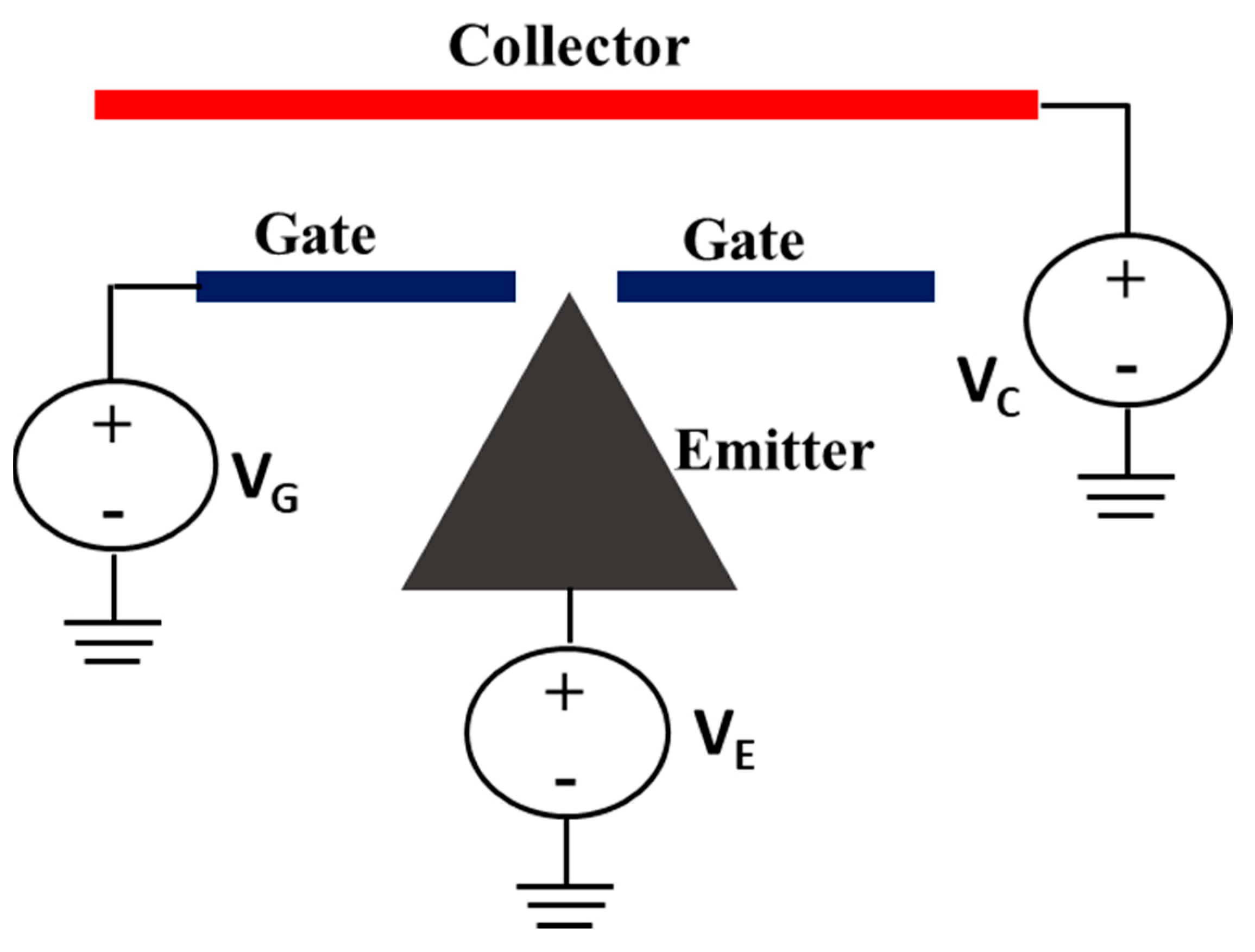
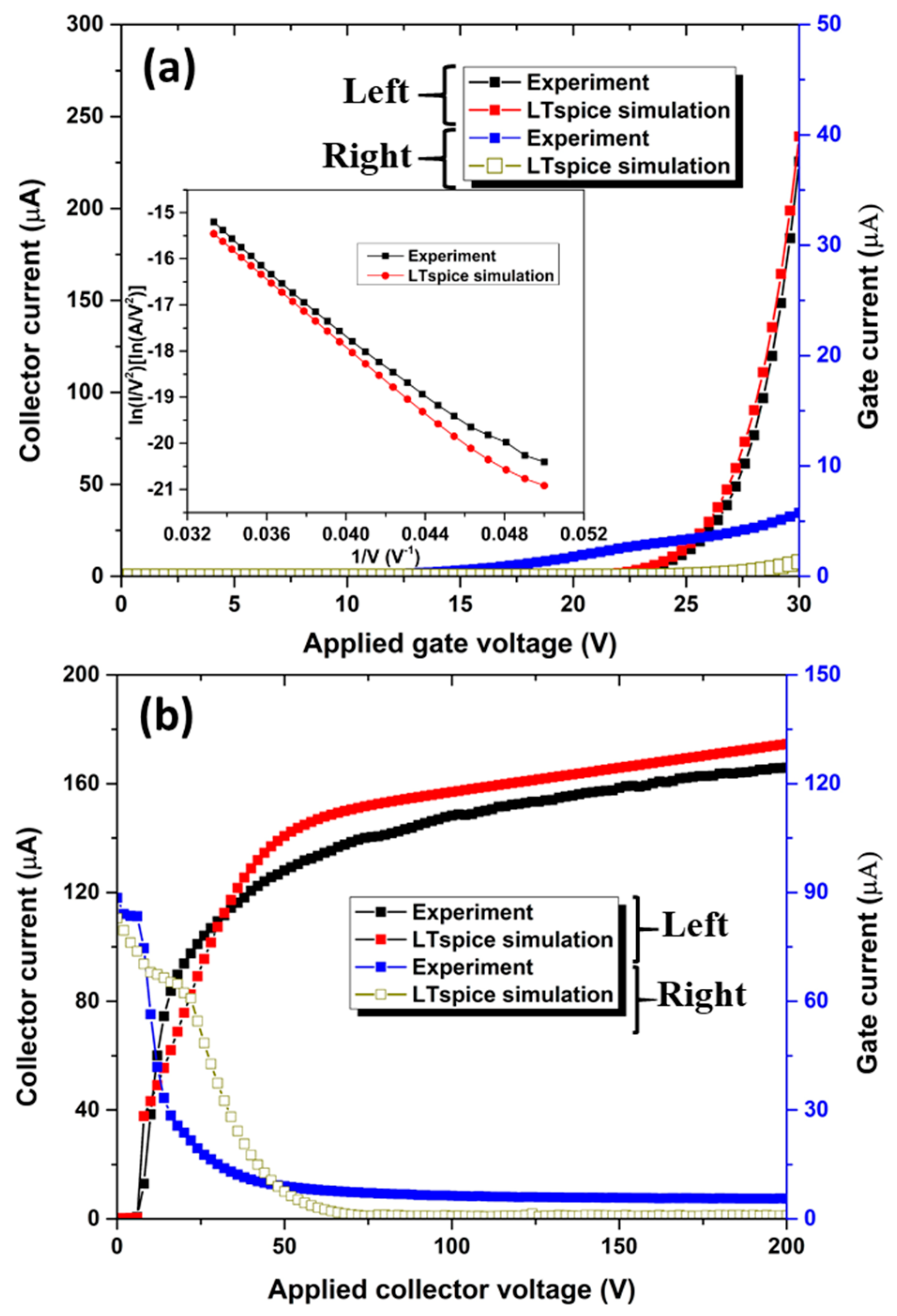
2. I-V Characterization Experiment
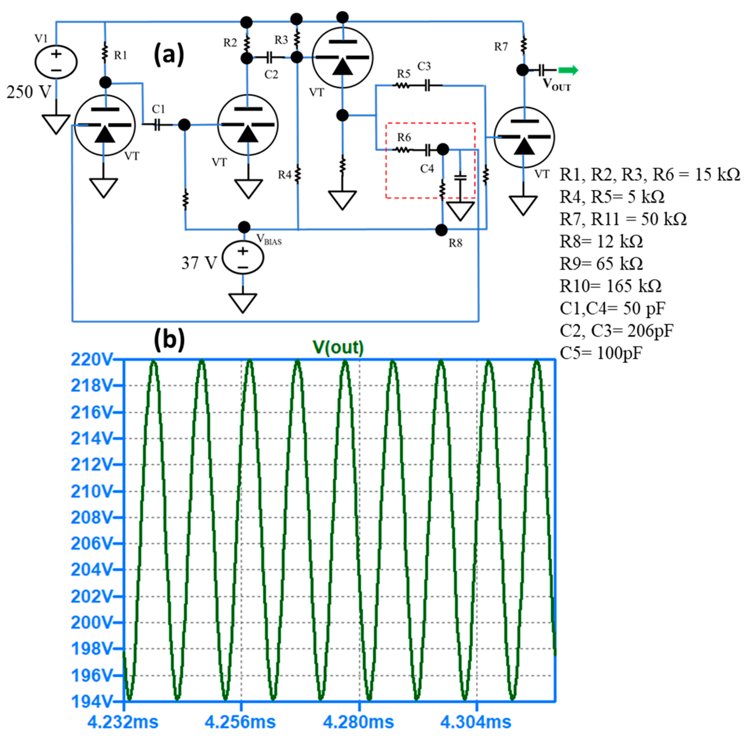
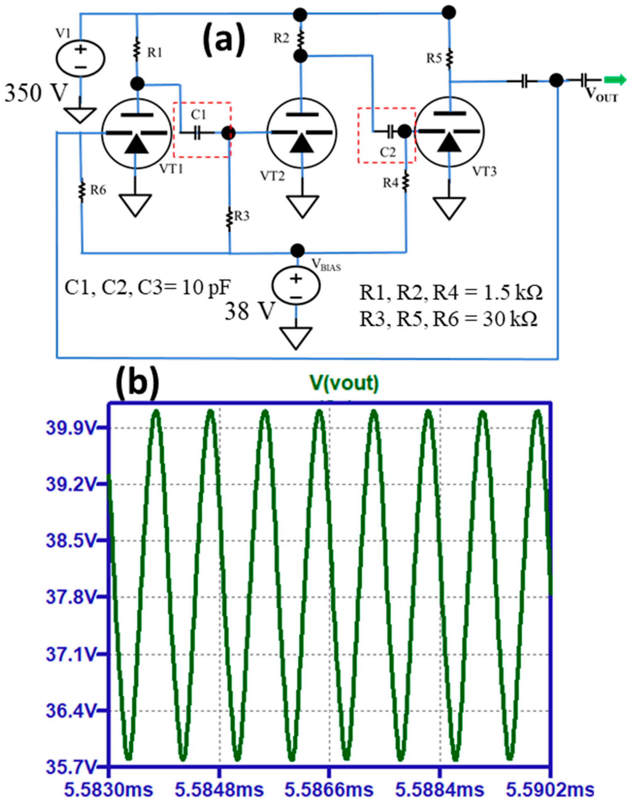
To establish a simulation model, I-V characterization experiments were carried out using a 1000 × 1000 silicon-gated field emitter array (Si-GFEAs) [14]. The gap between each tip is 1 μm, and the total number of tips are 1 million. These GFEAs include self-aligned polysilicon gates (gate aperture ≈ 300 nm), and each tip is supported by silicon nanowires at the bottom, which have a diameter of 150 nm and a height of 10 μm. These nanowires act as ballast resistors. Detailed fabrication methods and device descriptions can be found elsewhere [6]. The 1000 × 1000 arrays were able to produce a current density greater than 100 A/cm2 [14], which made these a clear choice for the experiments. I–V characterization experiments were executed in a high vacuum environment created in a stainless-steel test chamber. The high vacuum chamber is fitted with electrical feedthroughs and a three-axis manipulator probe arm, which was used to connect to the gate pads of the GFEAs. A Keysight B2902A source measurement unit was used to carry out the experiments. Elaborated test chamber setup and experimental details can be found in our previous works [7,19].
Figure 1 shows the experimental schematic structure. For the output characteristics, the VC was swept from 0 to 200 V, and for the transfer characteristics, the VG was swept from 0 to 40 V. For all the tests, VE was kept at the ground. The results were used to develop an appropriate VT model, and the details can be found in our previous work [17], where we developed, simulated, and experimentally validated a 152 kHz Colpitts oscillator. This validation provides confidence in our circuit design.
Figure 2a shows the transfer characteristics comparison data of experiment and model for a collector voltage of 200 V, and Figure 2b shows the output characteristics of experiment and LTspice model for a fixed gate voltage of 30 V. From Figure 2a, it can be observed that the device turns on at a gate voltage of approximately VG, ON = 24 V and reaches > 0.225 mA of current at VG = 30 V. From Figure 2a, it can be observed that experiment and model agree well. Figure 2a (inset) shows the Fowler–Nordheim (F–N) [11] plot for the gate sweep of 0 to 30 V. From Figure 2b, it can clearly be observed that the data of the experiment and model results match well. Please note that, for the model development, a gate voltage of 40 V was used, and the details can be found in our previous work [17].

3. Simulation Model

The Fowler–Nordheim (F–N) model was used to establish the VT model [11,20,21,22]. The F–N equation is given as
I = a F N V G 2 exp b F N V G
Here, VG is applied gate potential in V, aFN and bFN are F-N coefficients and are defined as follows:
ln I V G 2 = ln a F N b F N V G
b F N = 0.95 · 6.83 × 10 7 · φ 3 2 β
where φ is the emitter work function (eV), and β is the field enhancement factor. Here, the work function is assumed to be 4.05 eV for Si. Further, to predict the model accurately, a hyperbolic tangent or tanh function was incorporated [17].
The model provides [17]
I C , M o d e l = I E , M o d e l · 0.5 · 1 + tan h V C d e
where the parameters d and e (two sets of coefficients for tanh) are dependent on VG. IC is = collector current (A), and IE is = emitter current (A). A detailed model development method can be found in our previous work [17].
Figure 3 shows the circuit diagram and the temporal response characteristics of a VT-based Wien oscillator circuit. The Wien oscillator [23,24] is based on a frequency-selective form of the Wheatstone bridge circuit [25]. The Wien Bridge Oscillator is a two-stage RC coupled amplifier circuit that has good stability at its resonant frequency and low distortion. The Wien Bridge Oscillator uses a feedback circuit consisting of a series RC circuit connected with a parallel RC of the same component values, producing a phase delay or phase advance circuit depending upon the frequency. Figure 3a shows the Wien oscillator circuit along with the values of the passive components, where V1 = 250 V and VBIAS = 37 V. Figure 3b shows the temporal response of the Wein oscillator simulation circuit. The observed oscillation frequency is ≈102 kHz with a VPP of ≈26 V. The circuit includes four VTs. Among the four VTs, the rightmost one is used as a load for the simulation.
Figure 4 shows the schematic and temporal response characteristics of the VT-based Ring oscillator circuit. The Ring oscillator [26] is a combination of inverters connected in series with a feedback connection. The output of the final stage is again connected to the initial stage of the oscillator. The values for the passive components that can be seen in Figure 4a,b show the temporal response of the Ring oscillator simulation circuit. The circuit is comprised of three VTs and passive components (resistors and capacitors). The applied V1 = 350 V and VBIAS = 38 V. Observed oscillation frequency is ≈ 1.12 MHz with a VPP of ≈ 4.5 V. The VPP of this Ring oscillator circuit could be limited by the RC delay caused by the device capacitance [17] and biasing resistors.
A simple NOR gate [27] can be constructed using resistor–transistor logic (RTL) switches connected together with the inputs connected directly to the transistor gates. The logic NOR gate’s output becomes “HIGH” only when both of its inputs are at “LOW” states, and for the rest of the states, the output will be in the “LOW” level state. A simple 2-input NOR gate was designed and simulated in LTspice using the VT model. Figure 5a shows the circuit where the inputs are connected directly to the transistor gates.
Both transistors must be cut off (“OFF”) for an output. Figure 5b shows the output waveform. The circuit is comprised of three VTs and passive components (resistors). From the output, it can clearly be seen that when both the inputs are low or “false”, the output is high or “true” and the output is low or “false” for all other cases, which clearly denotes the NOR operation. Here, the low-state voltage does not go to “0”. However, we can still achieve the NOR operation using the high or low output.
A simple NAND gate [27,28] can be constructed using resistor–transistor logic (RTL) switches connected together with the inputs connected directly to the transistor gates. The core logic is a NOR gate formed by U1 and U2 and converted to a NAND gate through DeMorgan’s Theorem [29], with the input inverters formed by U3 and U4 and an output inverter formed by U5. Figure 6a shows the circuit diagram, and Figure 6b shows the output waveform. The device is comprised of six VTs and passive components (resistors). From the output waveform, it can clearly be seen that the output is low only when both inputs are high. Otherwise, the output is always high, which clearly denotes a NAND gate operation. However, similar to the NOR gate, the “low” state does not go to “0” V. The NAND operation can still be achieved by setting the “low” and “high” threshold limits.

4. Conclusions

In summary, this study explores the modeling of a variety of VT-based circuits. In addition, and more importantly, we successfully simulated several oscillator and logic circuit designs based on an optimal VT. To the best of our knowledge, it is the first demonstration of a vacuum-state oscillator in the circuit simulation module in which the VT functions as a conventional triode or field-effect transistor (FET). Several circuits, a Wein oscillator, a Ring oscillator, a NOR gate, and a NAND circuit, were designed and demonstrated using LTspice simulations. The low-frequency Wein oscillator circuit has an oscillation frequency of 102 kHz with an amplitude of 26 Vpp. The Ring oscillator model showed a comparatively higher oscillation frequency of 1.14 MHz with a magnitude of 4 Vpp. These oscillators and logic circuits could be used as low-frequency harsh environment temperature, pressure, and vibration sensors in nuclear reactors, satellites, and spacecraft. Future work includes the experimental validation of these circuits.

Author Contributions

Methodology, R.B.; Software, R.H.; Validation, R.H. and J.B.; Investigation, R.B.; Resources, W.C. and G.R.; Data curation, R.B.; Writing—original draft, R.B.; Writing—review & editing, J.B.; Funding acquisition, A.I.A. and J.B. All authors have read and agreed to the published version of the manuscript.

Funding

This research was funded by the Air Force Office of Scientific Research under grant FA9550-18-1-0436.

Institutional Review Board Statement

Not applicable.

Informed Consent Statement

Not applicable.

Data Availability Statement

The data presented in this study are available in the article.

Conflicts of Interest

The authors declare no conflict of interest.

References

  1. Han, J.-W.; Moon, D.-I.; Meyyappan, M. Nanoscale Vacuum Channel Transistor. Nano Lett. 2017, 17, 2146–2151. [Google Scholar] [CrossRef] [PubMed]
  2. Han, J.-W.; Sub Oh, J.; Meyyappan, M. Vacuum Nanoelectronics: Back to the Future?—Gate Insulated Nanoscale Vacuum Channel Transistor. Appl. Phys. Lett. 2012, 100, 213505. [Google Scholar] [CrossRef]
  3. Injo, O.; Lee, C.; Seo, S.-C.; Kim, S. Vertical Vacuum Channel Transistor with Minimized Air Gap between Tip and Gate 2019. U.S. Patent US10431682B2, 23 April 2019. [Google Scholar]
  4. Park, I.J.; Jeon, S.-G.; Shin, C. A New Slit-Type Vacuum-Channel Transistor. IEEE Trans. Electron Devices 2014, 61, 4186–4191. [Google Scholar] [CrossRef]
  5. Srisonphan, S.; Jung, Y.S.; Kim, H.K. Metal–Oxide–Semiconductor Field-Effect Transistor with a Vacuum Channel. Nat. Nanotechnol. 2012, 7, 504. [Google Scholar] [CrossRef] [PubMed]
  6. Guerrera, S.; Akinwande, A.I. Nanofabrication of Arrays of Silicon Field Emitters with Vertical Silicon Nanowire Current Limiters and Self-Aligned Gates. Nanotechnology 2016, 27, 295302. [Google Scholar] [CrossRef] [PubMed]
  7. Bhattacharya, R.; Karaulac, N.; Chern, W.; Akinwande, A.; Browning, J. Temperature Effects on Gated Silicon Field Emission Array Performance. J. Vac. Sci. Technol. B 2021, 39, 023201. [Google Scholar] [CrossRef]
  8. Davidson, J.L.; Kang, W.P.; Subramanian, K.; Holmes-Siedle, A.G.; Reed, R.A.; Galloway, K.F. Diamond Vacuum Electronic Device Behavior after High Neutron Fluence Exposure. IEEE Trans. Nucl. Sci. 2009, 56, 2225–2229. [Google Scholar] [CrossRef]
  9. Kang, W.; Davidson, J.; Subramanian, K.; Choi, B.; Galloway, K. Nanodiamond Lateral VFEM Technology for Harsh Environments. IEEE Trans. Nucl. Sci. 2007, 54, 1061–1065. [Google Scholar] [CrossRef]
  10. Han, J.-W.; Oh, J.S.; Meyyappan, M. Cofabrication of Vacuum Field Emission Transistor (VFET) and MOSFET. IEEE Trans. Nanotechnol. 2014, 13, 464–468. [Google Scholar] [CrossRef]
  11. Fowler, R.H.; Nordheim, L. Electron Emission in Intense Electric Fields. Proc. R. Soc. London. Ser. A Contain. Pap. A Math. Phys. Character 1928, 119, 173–181. [Google Scholar]
  12. Han, J.-W.; Seol, M.-L.; Moon, D.-I.; Hunter, G.; Meyyappan, M. Nanoscale Vacuum Channel Transistors Fabricated on Silicon Carbide Wafers. Nat. Electron. 2019, 2, 405–411. [Google Scholar] [CrossRef]
  13. Ding, M.; Sha, G.; Akinwande, A.I. Silicon Field Emission Arrays with Atomically Sharp Tips: Turn-on Voltage and the Effect of Tip Radius Distribution. IEEE Trans. Electron Devices 2002, 49, 2333–2342. [Google Scholar] [CrossRef]
  14. Guerrera, S.A.; Akinwande, A.I. Silicon Field Emitter Arrays with Current Densities Exceeding 100 A/cm2 at Gate Voltages below 75 V. IEEE Electron Device Lett. 2015, 37, 96–99. [Google Scholar] [CrossRef]
  15. Kim, D.Y.; Kim, H.T. Vacuum Channel Transistor and Diode Emitting Thermal Cathode Electrons, and Method of Manufacturing the Vacuum Channel Transistor 2012. U.S. Patent US8159119B2, 17 April 2012. [Google Scholar]
  16. Schaller, R.R. Moore’s Law: Past, Present and Future. IEEE Spectr. 1997, 34, 52–59. [Google Scholar] [CrossRef]
  17. Bhattacharya, R.; Hay, R.; Cannon, M.; Karaulac, N.; Rughoobur, G.; Akinwande, A.I.; Browning, J. Demonstration of a Silicon Gated Field Emitter Array Based Low Frequency Colpitts Oscillator at 400 °C. J. Vac. Sci. Technol. B 2023, 41, 023201. [Google Scholar] [CrossRef]
  18. Xu, J.; Qin, Y.; Shi, Y.; Shi, Y.; Yang, Y.; Zhang, X. Design and Circuit Simulation of Nanoscale Vacuum Channel Transistors. Nanoscale Adv. 2020, 2, 3582–3587. [Google Scholar] [CrossRef]
  19. Bhattacharya, R.; Karaulac, N.; Rughoobur, G.; Chern, W.; Akinwande, A.I.; Browning, J. Ultraviolet Light Stimulated Water Desorption Effect on Emission Performance of Gated Field Emitter Array. J. Vac. Sci. Technol. B Nanotechnol. Microelectron. Mater. Process. Meas. Phenom. 2021, 39, 033201. [Google Scholar] [CrossRef]
  20. Murphy, E.L.; Good Jr, R. Thermionic Emission, Field Emission, and the Transition Region. Phys. Rev. 1956, 102, 1464. [Google Scholar] [CrossRef]
  21. Jensen, K.L. Improved Fowler–Nordheim Equation for Field Emission from Semiconductors. J. Vac. Sci. Technol. B Microelectron. Nanometer Struct. Process. Meas. Phenom. 1995, 13, 516–521. [Google Scholar] [CrossRef]
  22. Forbes, R.G. Renewing the Mainstream Theory of Field and Thermal Electron Emission. In Modern Developments in Vacuum Electron Sources; Springer: Berlin/Heidelberg, Germany, 2020; pp. 387–447. [Google Scholar]
  23. Holt, A.; Lee, M. A Class of RC Oscillators. Proc. IEEE 1967, 55, 1119. [Google Scholar] [CrossRef]
  24. Senani, R. New Types of Sinewave Oscillators. IEEE Trans. Instrum. Meas. 1985, IM-34, 461–463. [Google Scholar] [CrossRef]
  25. Hoffmann, K. Applying the Wheatstone Bridge Circuit; HBM: Darmstadt, Germany, 1974. [Google Scholar]
  26. Lee, S.-J.; Kim, B.; Lee, K. A Novel High-Speed Ring Oscillator for Multiphase Clock Generation Using Negative Skewed Delay Scheme. IEEE J. Solid-State Circuits 1997, 32, 289–291. [Google Scholar]
  27. Gate, B.N.; Gate, G.N.; Upper, U.I.L.I.O.; Gate, O.; Gate, N.; Gate, X.; Gate, X. Introduction to Digital Logic Design; University of California San Diego: La Jolla, CA, USA, 1993. [Google Scholar]
  28. Alipour-Banaei, H.; Serajmohammadi, S.; Mehdizadeh, F. All Optical NOR and NAND Gate Based on Nonlinear Photonic Crystal Ring Resonators. Optik 2014, 125, 5701–5704. [Google Scholar] [CrossRef]
  29. haq Shaik, E.; Rangaswamy, N. Realization of All-Optical NAND and NOR Logic Functions with Photonic Crystal Based NOT, OR and AND Gates Using De Morgan’s Theorem. J. Opt. 2018, 47, 8–21. [Google Scholar] [CrossRef]
Figure 1. Experimental schematic model showing emitter (E), gate (G), and collector (C).
Applsci 13 12807 g001
Figure 2. (a) Transfer characterization comparison between experiment and LTspice model (inset is the F-N plot) and gate current comparison. (b) Show the output characteristics and gate current comparison between experiment and model. Axis are marked with “Left” and “Right”.
Applsci 13 12807 g002
Figure 3. (a) LTspice model of three-device Wien oscillator circuit plus output buffer (rightmost VT) and (b) output waveform.
Applsci 13 12807 g003
Figure 4. (a) LTspice model of a three VT device Ring oscillator simulation circuit and (b) the simulated output waveform.
Applsci 13 12807 g004
Figure 5. (a) Two-device NOR gate plus simulated load. (b) Output of the NOR gate. The output is high when both the inputs are low, and the output is low for all the other cases.
Applsci 13 12807 g005
Figure 6. (a) Five-device NAND gate plus simulated load. (b) Output of the NAND gate. The output is low only when both the inputs are high; otherwise, the output is always high.
Applsci 13 12807 g006
Disclaimer/Publisher’s Note: The statements, opinions and data contained in all publications are solely those of the individual author(s) and contributor(s) and not of MDPI and/or the editor(s). MDPI and/or the editor(s) disclaim responsibility for any injury to people or property resulting from any ideas, methods, instructions or products referred to in the content.

