Article

The Low-Loss Spot Size Converter for Alignment with Cleaved Single Mode Fiber

The Key Laboratory of Specialty Fiber Optics and Optical Access Networks, School of Communication and Information Engineering, Shanghai University, Shanghai 200444, China
*
Authors to whom correspondence should be addressed.
Appl. Sci. 2023, 13(14), 8157; https://doi.org/10.3390/app13148157
Submission received: 9 June 2023 / Revised: 7 July 2023 / Accepted: 10 July 2023 / Published: 13 July 2023

Abstract

:
Integrating the graded index (GRIN) waveguide with the 2-D inversely-tapered waveguide, a new design of spot size converter (SSC) has been proposed to couple the light beam between the cleaved single-mode fiber (SMF) and the silicon (Si) wire waveguide on the silicon-on-insulator (SOI) platform. The device demonstrates a low coupling loss of 0.27 dB when it is coupled to a cleaved SMF. The polarization-dependent loss (PDL) is less than 0.25 dB, and the 1-dB alignment tolerance is about −2.0~2.0 µm for both vertical and horizontal directions. At the same time, the starting tip width of the tapered waveguide is kept at the level of the lithography limitation at the current commercial silicon photonics fab. This integrated SSC could be an improved design for reducing the coupling loss between the cleaved SMF and the Si waveguide.

1. Introduction

The SOI platform has emerged as an important platform for photonic integrated circuits (PIC), which could integrate conventional optical devices onto silicon wafers. Silicon photonic chips based on SOI platform fabrication, whose manufacturing process is compatible with the complementary metal oxide semiconductor (CMOS) process, can realize optoelectronic hybrid integration on a single chip, which has an important role in optical communication networks. The mode field size of the Si waveguide on this platform is at the submicron level, while the mode field diameter (MFD) of the cleaved SMF is typically in the 8~10 µm range. The direct fiber-to-chip coupling presents significant losses due to the mode mismatch. Therefore, fiber-to-chip couplers play an essential role in the SOI platform, which is divided into two models: vertical grating couplers and SSCs. Compared with vertical grating couplers, SSCs demonstrate lower coupling loss and lower polarization-dependent loss (PDL) [1]. Moreover, the SSC is more conducive to the packaging of commercial silicon photonic chips. Therefore, SSCs may be more suitable for implementing fiber-to-chip coupling for commercial PIC products.
The typical SSC contains a tapered Si waveguide and SiO2 cladding. Along the transmission direction, as the Si waveguide cross-section increases, the mode field is gradually guided into the Si waveguide [2,3]. In addition to the traditional tapered waveguides, other structures were applied to SSCs for lower coupling losses. The coupling loss of the following SSCs is obtained at a wavelength of 1550 nm. The structure with multiple taper tips was used to couple with a lensed fiber (MFD: 6 µm), and the coupling loss is 1.25 dB [4]. Subwavelength grating structures were utilized to reduce the device size and the coupling loss with lensed fibers or ultra-high numerical aperture (UHNA) fibers (MFD: <6 µm), and the minimum coupling loss could be less than 0.42 dB [5,6]. Most SSCs were coupled with lensed fibers or UHNA fibers because the MFD of lensed fibers and UHNA fibers can be less than 6 µm, which matches the size of the mode field at the starting position of SSCs [7]. Compared to cleaved SMFs, lensed fibers are expensive to fabricate and can be easily damaged. In order to reduce coupling difficulty and costs, one of the trends in SSCs is to change from alignment with lensed fibers to alignment with cleaved SMFs. When coupling with the cleaved SMF, the coupling loss of SSC using an inversely-tapered Si waveguide is up to 3.5 dB for transverse electric (TE) mode [8]. To reduce the coupling loss, additional structures are usually required besides the tapered Si waveguide, such as subwavelength grating structures [5], overlapped tapers [9], thin-film stack-based lenses [10], and polymer tapered waveguides [11]. However, the coupling loss of SSC when coupling with cleaved SMF is difficult to achieve below 1 dB. Although the coupling loss between SSCs and cleaved SMFs can be as low as 0.75 dB using a subwavelength grating structure, the length of the device is more than 1500 µm, which is hard for the integration with other devices on the single chip [5]. It can be seen that achieving low-loss coupling between SSC and cleaved SMF is difficult. In addition to this, the tapered waveguides in SSCs typically have taper tips smaller than 200 nm, which is not suitable for SSCs to be fabricated at the current commercial silicon photonics fab.
In this paper, a design of SSC integrating the ion-implanted GRIN waveguide and the 2-D inversely-tapered waveguide has been proposed for coupling the light between the cleaved SMF (MFD: 8~10 µm) and the Si waveguide. The tip width of the tapered waveguide is 200 nm and the height is 60 nm, which is compatible with commercial silicon photonics technology. The coupling loss of the SSC is obtained by using finite difference time domain (FDTD) simulation. When the MFD is 8 µm and the wavelength is 1550 nm, the lowest coupling loss is 0.29 dB for TE mode and 0.27 dB for transverse magnetic (TM) mode. Meanwhile, the starting Si tip width of 200 nm reaches the level manufactured at the commercial silicon photonics fab.

2. Design of Materials and Methods

The scheme of the SSC is shown in Figure 1. The SSC consists of the ion-implanted GRIN waveguide and the 2-D inversely-tapered waveguide. The GRIN waveguide compresses the mode field with 8~10 µm MFD of the cleaved SMF into a small mode field with 3~4 µm MFD, both horizontally and vertically. As shown in Figure 1, closely following the GRIN waveguide is the 2-D inversely-tapered waveguide, which could convert the small mode field with 3~4 µm MFD into the fundamental mode of the Si waveguide adiabatically. The 2-D inversely-tapered waveguide is located above the buried oxygen (BOX) layer. Details about the design will be explained in the following sections.

2.1. GRIN Waveguide

GRIN waveguides have a gradual refractive index distribution, and light beams transmitted within GRIN waveguides could be compressed or enlarged [12]. In this paper, the refractive index profile of the ion-implanted GRIN waveguide is a symmetric Gaussian profile in the horizontal direction, as shown in Figure 2b. The refractive index profile is a half-parabolic profile in the range of 0~9 µm and a Gaussian profile in the range of 9~11 µm in the vertical direction as shown in Figure 2c.
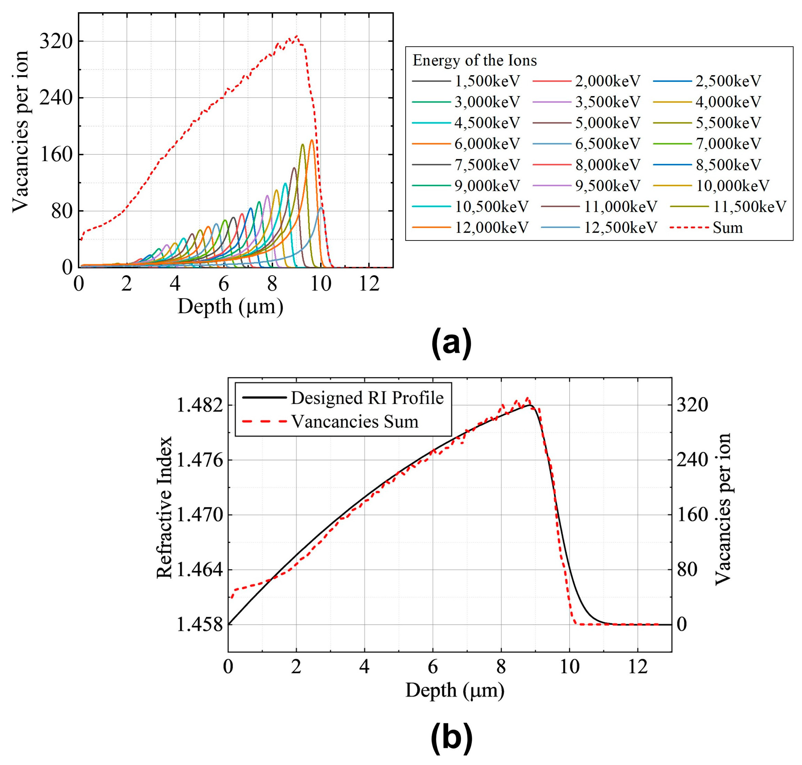
Here, we give the theory of using ion implantation technology to fabricate the GRIN waveguide of our design. Ion implantation is a mature technique for waveguide fabrication in the field of integrated optics, that is compatible with current commercial silicon photonics technology [13]. Ion implantation can precisely change the refractive index of the material by controlling the type of ions, ions energy, and ions dose. Ion energy can range from several thousand electron volts to over ten million electron volts [14]. In the vertical direction, a single ion implantation can form a Gaussian profile of the refractive index distribution, and with multiple ion implantations, it is possible to achieve a customized refractive index profile [15]. The lateral Gaussian distribution can be naturally formed by using a lithograph-defined window within the ion implantation [16]. Therefore, the control of the refractive index in the vertical direction is more important for the GRIN waveguide. As shown in Figure 3, the distribution of vacancies formed after multiple implantations of N+ into SiO2 simulated by the transport of ions in matter (TRIM) software could fit the refractive index profile of our designed GRIN waveguide, which demonstrates that our designed GRIN waveguide can be fabricated by multiple implantations of N+ into SiO2. The vacancy distribution could linearly fit the refractive index distribution within the error tolerance after annealing [17]. Therefore, the refractive index distribution formed by the N+ implanted into the SiO2 can be predicted by the vacancy distribution obtained from the TRIM simulation. For the type of ions, N+ implanted into SiO2 can increase the refractive index of SiO2 by up to 6%. Therefore, the refractive index range is from 1.458 to 1.482 in our design. In addition to this, ion implantation introduces a high-temperature annealing process [17]. Therefore, the subsequent high-temperature environment will not affect the refractive index profile of the GRIN waveguide fabricated by ion implantation, which is beneficial for achieving optical integration.
Here, the route of the light rays in the GRIN waveguide with a parabolic refractive index profile could be analyzed according to the geometric optics propagation theory [12]:
y = y 0 c o s ( A z ) + t a n θ A s i n ( A z )
where y 0 and θ are the incident position and the angle of incidence of the light rays, respectively. A is a constant related to n m a x , n 0 , and h 0 . Their relationship is described by:
A = 2 h 0 2 ( 1 n 0 n m a x )
where n m a x is the maximum refractive index, and n 0 is the refractive index of SiO2, h 0 is the thickness of the waveguide. According to Equation (1), when the angle of incidence of light rays is zero radians, regardless of whether the refractive index profile of the GRIN medium is parabolic or half-parabolic, the route of light rays within the GRIN medium is a sinusoidal function with a period P [12]. P is represented by:
P = 2 π A
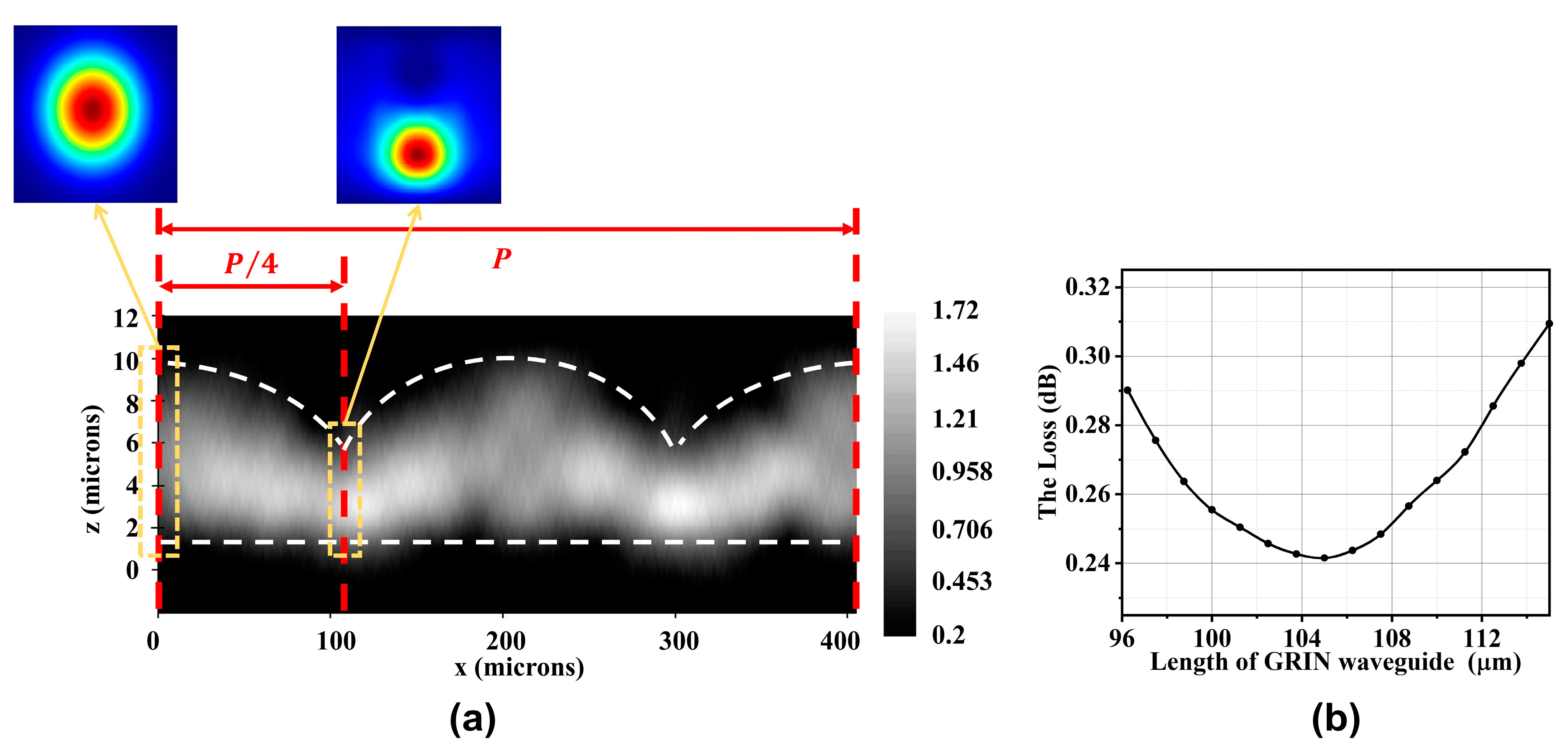
As shown in Figure 4a, when the light ray is incident vertically to the end face of the GRIN (with an incidence angle of 0), the periodic focus occurs at the focal position P l :
P l = ( 2 l 1 ) 4 P , l = 1 , 2 , 3 ,
Obviously, the first focused position of light rays is at a distance of P / 4 according to Equation (4), and it is clear that the mode field size is the smallest at this position. Therefore, the shortest length of the GRIN waveguide should be set as P / 4 . Combining Equations (2) and (3), the shortest length of the GRIN waveguide can be predicted by:
l = P 4 = π 2 A = h 0 π 4 2 n m a x n m a x n 0
The MFD of the light source was set to 8 µm, and the simulation of the GRIN waveguide was performed via FDTD software. As shown in Figure 4b, the loss from the cleaved SMF to the beginning of the 2-D inversely-tapered waveguide can be as low as 0.24 dB when the GRIN waveguide length is 105 µm. When h 0 is 11.8 µm, n m a x is 1.46, and n 0 is 1.458, the length calculated by Equation (5) is 99 µm, which is close to the optimized length (105 µm) by 3D-FDTD simulation.
From the cleaved SMF to the taper tip position of the 2-D inversely-tapered waveguide, this part is the GRIN waveguide section, and the loss of the GRIN waveguide section consists of three parts. The first part of the loss is the reflection loss between the cleaved SMF and the GRIN waveguide, which could be minimized by the selection of a suitable refractive index matching liquids [8]. The second part of the loss is the transmission loss of the GRIN waveguide. The transmission loss is generally small and is neglected according to the 3D-FDTD simulations. The third part of the loss is the mode mismatch loss between the GRIN waveguide and the 2-D inversely-tapered waveguide, which is the main source of the loss. Therefore, reducing the mode mismatch loss is the focus of our discussion. Making the effective refractive indices of the two modes close to each other is an effective way to reduce the mode mismatch loss. The refractive indices and dimensions of Cladding 1 and Cladding 2 have been optimized in order to make the effective refractive index of the fundamental mode of the 2-D inversely-tapered waveguide close to that of the mode at the end of the GRIN waveguide. In theory, the mode overlap integral can represent the mode mismatch loss to a certain extent. The modal overlap integral can be calculated by [5]:
η = | E 1 E 2 d A | 2 | E 1 | 2 d A | E 2 | 2 d A
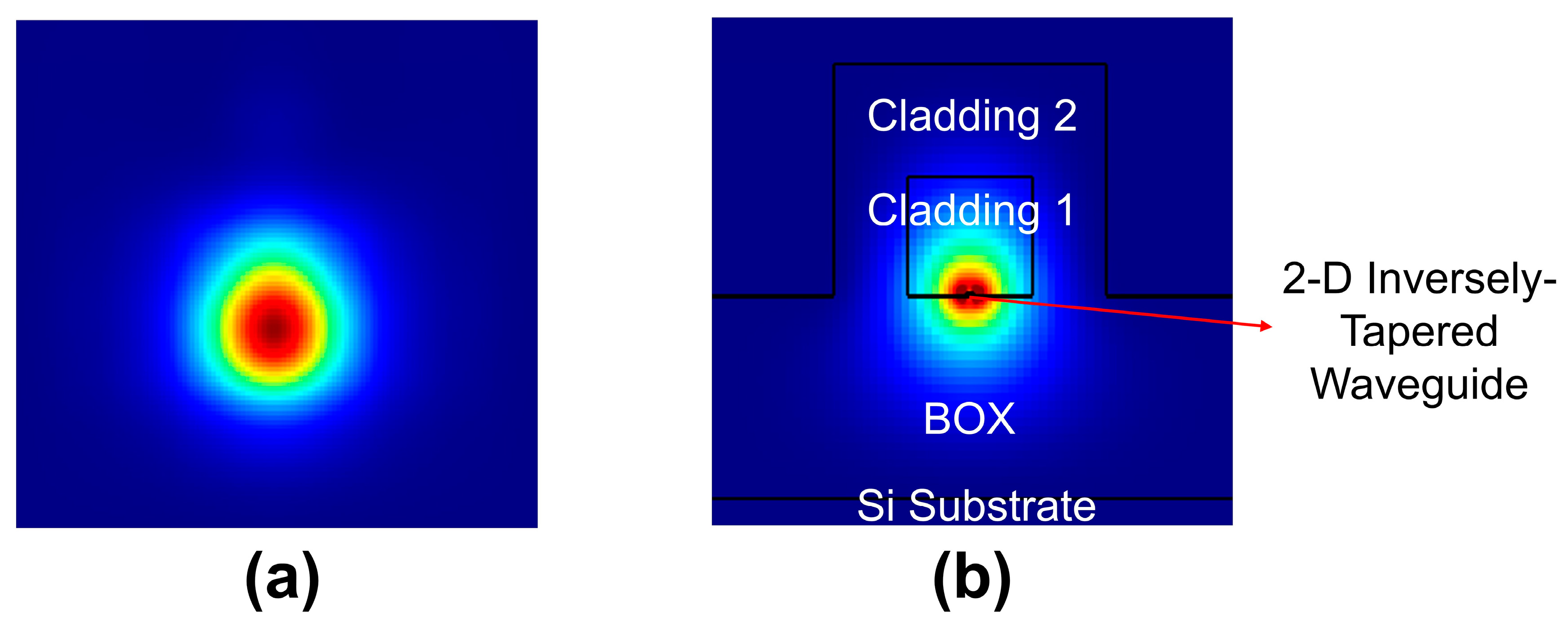
where E 1 and E 2 are the complex electric fields for the mode at the output end of the GRIN waveguide (Figure 5a) and the TE fundamental mode at the starting tip of the 2-D inversely-tapered waveguide section (Figure 5b), respectively. Due to the fact that Equation (6) only considers the electric field and does not take into account other factors such as refractive indices or the contribution of higher-order modes, there is a certain error between the mode mismatch loss calculated by Equation (6) and the loss obtained by 3D-FDTD. The loss obtained by 3D-FDTD is 0.24 dB, while the mode mismatch loss calculated by Equation (6) is 0.41 dB.

2.2. The 2-D Inversely-Tapered Waveguide

Inversely-tapered waveguides are usually used to couple light with mode fields of different spot sizes and shapes [2]. When the mode field from the cleaved SMF is incident on SSCs, the mode field will be smoothly guided into the Si waveguide as the Si waveguide cross-section increases. In order to reduce the loss, the design of the tapered Si waveguide needs to comply with the adiabatic transmission principle [18]. In addition to this, the roughness of the taper waveguide’s surface could lead to scattering losses in fabrication. The scattering loss of the Si waveguide could be as low as 0.5 dB/cm [19]. The length of our designed device is relatively short, so the scattering loss is negligible in the simulation.
The structure of the 2-D inversely-tapered waveguide is shown in Figure 6. The tapered waveguide tip width is 200 nm and the height is 60 nm in our design. Along the beam propagation direction, the width/height of the waveguide increase linearly to 500 nm/220 nm. The narrowest width of the tapered waveguide is set at 200 nm to be compatible with the level of lithography limitation at the current commercial silicon photonics fab [20]. The technology for fabricating linearly-tapered waveguides in the horizontal direction is mature. Silicon structures in the vertical direction can also be fabricated by gray-scale technology [21]. Grayscale technology refers to the introduction of gray-scale masks in reactive ion etching (RIE) to control the etching depth at different positions so as to realize the fabrication of Si waveguide structures in the vertical direction, which has been used in industrial manufacturing to fabricate micro-optical devices due to the low cost and the mature process [22]. Therefore, the linearly-tapered structure in the vertical direction in the 2-D inversely-tapered waveguide could be fabricated at a low cost by using gray-scale masks in RIE. Outside the 2-D inversely-tapered waveguide, two SiO2 cladding layers with different refractive indices were designed, which can both be accurately defined by plasma-enhanced chemical vapor deposition (PECVD) [23,24].
In our design, the length of the 2-D inversely-tapered waveguide has been optimized by eigenmode expansion (EME) simulation and was double-verified by 3D-FDTD simulation for comparison. The EME simulation could calculate the mode propagation coefficients for each part of the waveguide, which could optimize the length of the tapered waveguide to enable adiabatic transmission. As shown in Figure 7a, for the TM mode, the coupling loss is close to the minimum when the length of the tapered waveguide exceeds 200 µm. In order to make the coupling loss also close to the minimum for the TE mode, the optimal length of the tapered waveguide can be set to 300 µm. At this optimized length, it can be obtained that the loss of TE mode is 0.12 dB and the loss of TM mode is 0.05 dB for the full structure of the 2-D inversely-tapered waveguide.
The refractive indices and dimensions of the Cladding 1 and Cladding 2 have been specially optimized in order to reduce the mode mismatch loss between the GRIN waveguide and the 2-D inversely-tapered waveguide. The optimized refractive index difference between Cladding 1 and Cladding 2 is as small as 0.002. By using the radiofrequency PECVD technique, the refractive index of the deposited SiO2 can be controlled with extremely high precision [24], which could meet the requirement of depositing two SiO2 layers with a refractive index difference of 0.002. We also discussed the effect of increasing the refractive index difference on the coupling loss of the device. The refractive index of Cladding 2 is set to n , and in the paper, n is fixed at 1.458. The refractive index of Cladding 1 is set to n + n , n represents the refractive index difference between Cladding 1 and Cladding 2. The MFD of the light source is set to 8 µm, and the mode is TE mode. The coupling loss variation of the full SSC has been simulated when n varies between 0.002 and 0.017. According to Figure 7b, the coupling loss of the SSC increases with the increase in n . The coupling loss of the SSC can be maintained at less than 0.98 dB when n is less than 0.015, which demonstrates an acceptable fabrication tolerance for the device.

3. Results

The whole mode field distributions in the SSC are shown in Figure 8. The MFD of the light source is set to 8 µm and 10 µm, and the wavelength is set to 1550 nm. The simulation results of the SSC are presented by the FDTD solution using the Lumerical software. It can be seen that the beam is finally coupled from the cleaved SMF into the Si waveguide through the SSC. The coupling loss of the TE mode is 0.29 dB, and that of the TM mode is 0.27 dB for the light source with an 8 µm MFD. When the MFD of the light source is set to 10 µm, the coupling loss is limited to 0.58 dB for TE mode and 0.56 dB for TM mode. The simulation results show that the proposed SSC achieves a very low coupling loss of 0.27 dB with a cleaved SMF, and the good simulation results provide a basis for fabricating a low-loss SSC for alignment with a cleaved SMF.
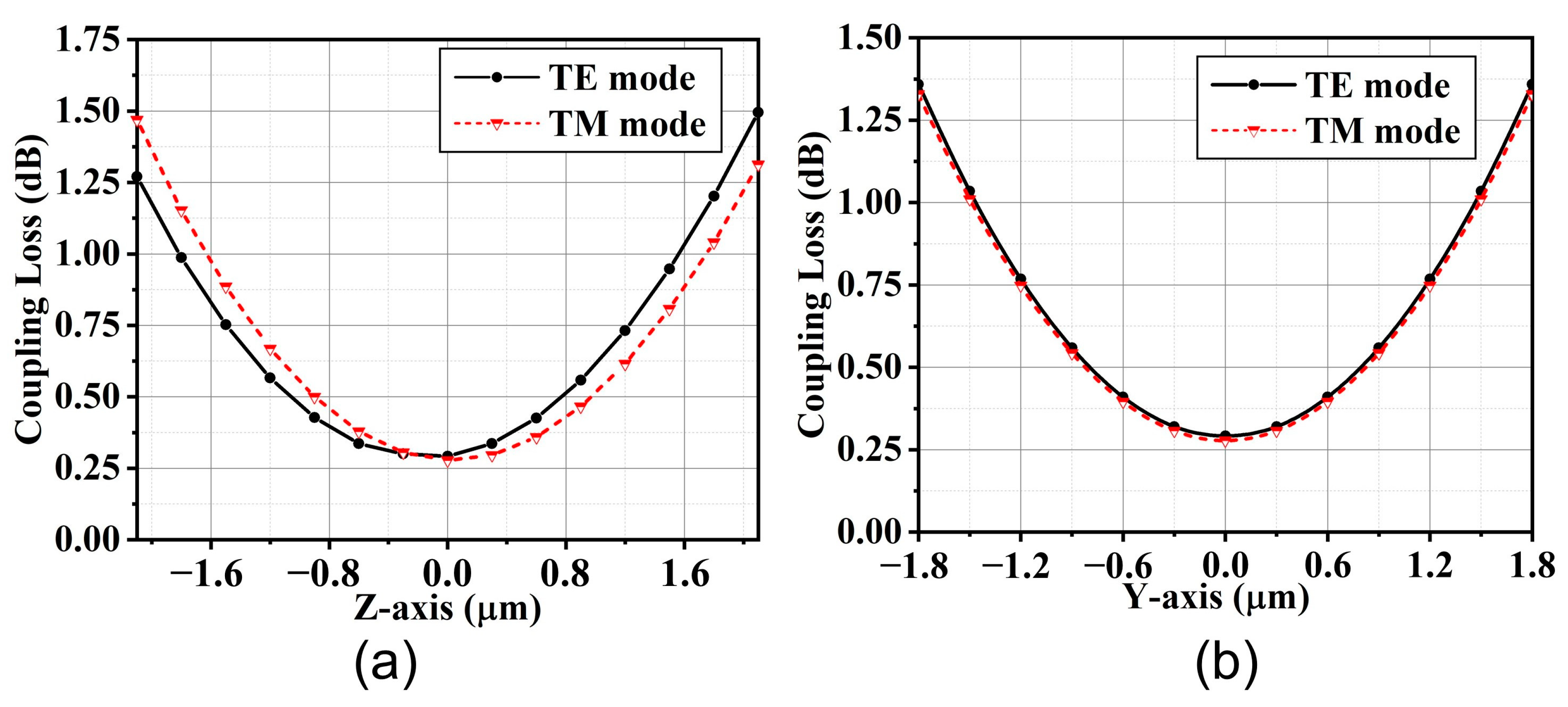
In addition to low coupling loss, the SSC we designed has a low PDL and large alignment tolerances. Figure 9 shows the simulation results of the 1-dB alignment tolerances at the MFD of 8 µm. For TE mode, the tolerance is −2.1 µm~1.9 µm in the vertical direction (Z-axis) and −1.8 µm~1.8 µm in the horizontal direction (Y-axis). For TM mode, the tolerance is −1.9 µm~2.1 µm in the vertical direction (Z-axis) and −1.8 µm~1.8 µm in the horizontal direction (Y-axis). The PDL between the two polarization states is less than 0.25 dB, which demonstrates good polarization insensitivity.
The conventional SSCs align with the lensed fiber, which increases the difficulty of alignment and inhibits large alignment tolerances. Therefore, one of the trends in SSC is to change from alignment with lensed fibers to alignment with cleaved SMFs. Table 1 shows the comparison between our work and other SSCs aligned with cleaved SMFs (MFD: 8~10 µm). Comparing with other SSCs, our designed SSC achieves lower loss coupling between the cleaved SMF and Si waveguides while maintaining the tapered waveguide tip width of 200 nm. This demonstrates the possibility of mass production of our proposed SSC on the current commercial silicon photonics fab, thus reducing the cost.

4. Conclusions

In this paper, a new design of low-loss SSC based on the integration of the ion-implanted GRIN waveguide and the 2-D inversely-tapered waveguide has been proposed and demonstrated. The SSC could be used for low-loss coupling with cleaved SMF. For the light beam with a MFD of 8 µm, the TE or TM coupling loss is 0.29 dB or 0.27 dB. For the light beam with a MFD of 10 µm, the TE or TM coupling loss is 0.58 dB or 0.56 dB. The device also demonstrated polarization insensitivity with a PDL of less than 0.25 dB. The 1-dB alignment tolerance is ~2.0 µm for the vertical direction or horizontal direction under TE or TM mode illuminations, which provides a large tolerance for the alignment with the cleaved SMF. For the 2-D inversely-tapered waveguide, the coupling loss could still be less than 1 dB when the refractive index difference between Cladding 1 and Cladding 2 is up to 0.015, which shows an acceptable tolerance for the device fabrication.
Comparing with the high-cost electron beam lithography technique, the manufacturing technology employed in our designed SSC could involve grayscale technology for micro-optical device fabrication and multiple ion implantation for customized refractive index waveguide fabrication, both of which are relatively mature at this moment. Moreover, the tapered waveguide tip width of 200 nm could allow the SSC to be fabricated in current commercial silicon photonics fabs. Therefore, we believe that this SSC could be manufactured at a lower cost. In the future, we will use the above-mentioned technologies to fabricate the real SSC, and the coupling loss will be characterized experimentally.

Author Contributions

Conceptualization, J.Z. and N.Y.; methodology, J.Z. and N.Y.; software, J.Z. and Z.W.; validation, J.Z. and Z.W.; formal analysis, J.Z.; investigation, J.Z.; resources, J.Z.; data curation, J.Z. and Z.W.; writing—original draft preparation, J.Z.; writing—review and editing, J.Z. and N.Y.; visualization, J.Z.; supervision, N.Y.; project administration, F.P. and Y.S.; funding acquisition, F.P., Y.S. and N.Y. All authors have read and agreed to the published version of the manuscript.

Funding

This research was funded by the National Key Research and Development Program of China (grant number 2019YFB1802901); and the Natural Science Foundation of China (NSFC) (grant number 62175143).

Institutional Review Board Statement

Not applicable.

Informed Consent Statement

Not applicable.

Data Availability Statement

Not applicable.

Acknowledgments

We also thank Di Ji for providing guidance on writing.

Conflicts of Interest

The authors declare no conflict of interest.

References

  1. Marchetti, R.; Lacava, C.; Carroll, L.; Gradkowski, K.; Minzioni, P. Coupling strategies for silicon photonics integrated chips. Photon. Res. 2019, 7, 201–239. [Google Scholar] [CrossRef]
  2. Kasaya, K.; Mitomi, O.; Naganuma, M.; Kondo, Y.; Noguchi, Y. A simple laterally tapered waveguide for low-loss coupling to single-mode fibers. IEEE Photon. Technol. Lett. 1993, 5, 345–347. [Google Scholar] [CrossRef]
  3. Larrea, R.; Gutierrez, A.M.; Griol, A.; Brimont, A.; Sanchis, P. Fiber-to-Chip Spot-Size Converter for Coupling to Silicon Waveguides in the O-Band. IEEE Photon. Technol. Lett. 2019, 31, 31–34. [Google Scholar] [CrossRef]
  4. He, A.; Guo, X.; Wang, K.; Zhang, Y.; Su, Y. Low Loss, Large Bandwidth Fiber-Chip Edge Couplers Based on Silicon-on-Insulator Platform. J. Lightwave Technol. 2020, 38, 4780–4786. [Google Scholar] [CrossRef]
  5. Papes, M.; Cheben, P.; Benedikovic, D.; Schmid, J.H.; Pond, J.; Halir, R.; Ortega-Moñux, A.; Wangüemert-Pérez, G.; Ye, W.N.; Xu, D.; et al. Fiber-chip edge coupler with large mode size for silicon photonic wire waveguides. Opt. Express 2016, 24, 5026–5038. [Google Scholar] [CrossRef]
  6. Xiao, Y.; Xu, Y.; Dong, Y.; Zhang, B.; Ni, Y. A 60 μm-Long Fiber-to-Chip Edge Coupler Assisted by Subwavelength Grating Structure with Ultralow Loss and Large Bandwidth. Photonics 2022, 9, 413. [Google Scholar] [CrossRef]
  7. Almeida, V.R.; Panepucci, R.R.; Lipson, M. Nanotaper for compact mode conversion. Opt. Lett. 2003, 28, 1302–1304. [Google Scholar] [CrossRef]
  8. Galán, J.V.; Sanchis, P.; Sánchez, G.; Martí, J. Polarization insensitive low-loss coupling technique between SOI waveguides and high mode field diameter single-mode fibers. Opt. Express 2007, 15, 7058–7065. [Google Scholar] [CrossRef]
  9. Fang, Q.; Song, J.; Luo, X.; Tu, X.; Jia, L.; Yu, M.; Lo, G. Low Loss Fiber-to-Waveguide Converter With a 3-D Functional Taper for Silicon Photonics. IEEE Photon. Technol. Lett. 2016, 28, 2533–2536. [Google Scholar] [CrossRef]
  10. Loh, T.; Wang, Q.; Ng, K.; Lai, Y.; Ho, S. CMOS compatible integration of Si/SiO2 multilayer GRIN lens optical mode size converter to Si wire waveguide. Opt. Express 2012, 20, 14769–14778. [Google Scholar] [CrossRef]
  11. Kobayashi, Y.; Sakaguchi, Y.; Yasuhara, K.; Ishigure, T. Mosquito method based polymer tapered waveguide as a spot size converter. Opt. Express 2021, 29, 9513–9531. [Google Scholar] [CrossRef]
  12. Delage, A.; Janz, S.; Xu, D.X.; Dalacu, D.; Lamontagne, B.; Bogdanov, A.L. Graded-index coupler for microphotonic SOI waveguides. In Proceedings of the Photonics North 2004: Optical Components and Devices, Ottawa, ON, Canada, 20 December 2004. [Google Scholar] [CrossRef]
  13. Chen, F.; Wang, X.; Wang, K. Development of ion-implanted optical waveguides in optical materials: A review. Opt. Mater. 2007, 29, 1523–1542. [Google Scholar] [CrossRef]
  14. Pezzagna, S.; Naydenov, B.; Jelezko, F.; Wrachtrup, J.; Meijer, J. Creation efficiency of nitrogen-vacancy centres in diamond. New J. Phys. 2010, 12, 065017. [Google Scholar] [CrossRef]
  15. Márquez, H.; Salazar, D.; Rangel-Rojo, R.; Angel, J.L.; Vázquez, G.V.; Flores-Romero, E.; Rodríguez-Fernández, L.; Oliver, A. Waveguides by multiple implantations of Ag ion on SiO2 substrates. In Proceedings of the 22nd Congress of the International Commission for Optics: Light for the Development of the World, Puebla, Mexico, 25 October 2011. [Google Scholar] [CrossRef]
  16. Matsumura, H.; Furukawa, S. Theoretical considerations in lateral damage distribution formed by ion-implantation. Jpn. J. Appl. Phys. 1975, 14, 1783–1790. [Google Scholar] [CrossRef]
  17. Faik, A.B.; Chandler, P.J.; Townsend, P.D.; Webb, R. Refractive index changes formed by N+ implants in silica. Radiat. Eff. Defects Solids. 1986, 98, 233–241. [Google Scholar] [CrossRef]
  18. Fu, Y.; Ye, T.; Tang, W.; Chu, T. Efficient adiabatic silicon-on-insulator waveguide taper. Photon. Res. 2014, 2, A41–A44. [Google Scholar] [CrossRef]
  19. Lee, K.K.; Lim, D.R.; Kimerling, L.C.; Shin, J.; Cerrina, F. Fabrication of ultralow-loss Si/SiO2 waveguides by roughness reduction. Opt. Lett. 2001, 26, 1888–1890. [Google Scholar] [CrossRef]
  20. Teng, M.; Wu, H.; Li, C.; Wang, F.; Du, Y.; Zheng, X. O-Band Fiber-to-Chip Edge Coupler for High NA Fiber Based on a CMOS Compatible SOI Platform. In Proceedings of the 2022 Optical Fiber Communication Conference (OFC), San Diego, CA, USA, 6–10 March 2022. [Google Scholar] [CrossRef]
  21. Shiraishi, K.; Yoda, H.; Tsai, C.S. A two-port polarization-insensitive coupler module between single-mode fiber and silicon-wire waveguide. Opt. Express 2012, 20, 24370–24375. [Google Scholar] [CrossRef]
  22. Morgan, B.; Waits, C.M.; Krizmanic, J.; Ghodssi, R. Development of a deep silicon phase Fresnel lens using Gray-scale lithography and deep reactive ion etching. J. Microelectromech. Syst. 2004, 13, 113–120. [Google Scholar] [CrossRef]
  23. Liu, Y.; Li, Y.; Fan, Z.; Xing, B.; Yu, Y.; Yu, J. Fabrication and optical optimization of spot-size converters with strong cladding layers. J. Opt. A Pure Appl. Opt. 2009, 11, 085002. [Google Scholar] [CrossRef]
  24. Kim, Y.T.; Kim, D.S.; Yoon, D.H. PECVD SiO2 and SiON films dependant on the rf bias power for low-loss silica waveguide. Thin Solid Film. 2005, 475, 271–274. [Google Scholar] [CrossRef]
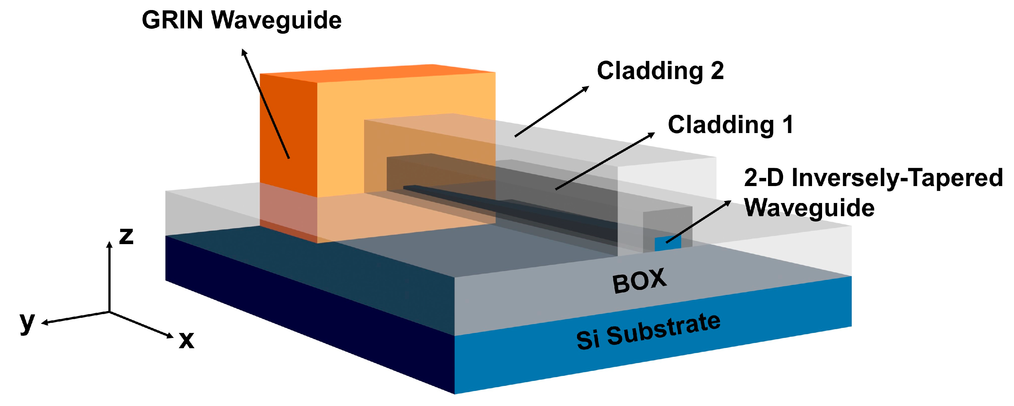
Figure 1. The scheme of the proposed SSC.
Applsci 13 08157 g001
Figure 2. Schematic and the refractive index transverse distribution of the GRIN waveguide. (a) The 3D view of the GRIN waveguide; (b) the refractive index profile in the horizontal direction (Y-axis); (c) the refractive index profile in the vertical direction (Z-axis).
Applsci 13 08157 g002
Figure 3. The vacancies distribution and the refractive index profile in the vertical direction. (a) The vacancies distribution calculated by TRIM for multiple ion implantations; (b) comparison of the refractive index profile designed by us and the sum vacancies distribution calculated by TRIM.
Applsci 13 08157 g003
Figure 4. The 3D-FDTD simulation results of the GRIN waveguide. (a) The mode field distribution of the GRIN waveguide; (b) the loss of the GRIN waveguide section as a function of the length of the GRIN waveguide.
Applsci 13 08157 g004
Figure 5. The field distributions of different modes. (a) The TE mode at the end face of the GRIN waveguide; (b) the fundamental TE mode at the beginning of the 2-D inversely-tapered waveguide.
Applsci 13 08157 g005
Figure 6. The scheme of the 2-D inversely-tapered waveguide. (a) With no cladding layer; (b) with Cladding 1 layer; (c) with Cladding 1 and Cladding 2 layers.
Applsci 13 08157 g006
Figure 7. The 3D-FDTD and EME simulation results of the 2-D inversely-tapered waveguide. (a) The coupling loss of the 2-D inversely-tapered waveguide as a function of the length of the 2-D inversely-tapered waveguide; (b) the coupling loss of the SSC as a function of n .
Applsci 13 08157 g007
Figure 8. The mode distribution of the SSC simulated by 3D-FDTD. (a) TE mode field distribution for 8 μm MFD; (b) TM mode field distribution for 8 μm MFD; (c) TE mode field distribution for 10 μm MFD; (d) TM mode field distribution for 10 μm MFD.
Applsci 13 08157 g008
Figure 9. The 1-dB alignment tolerance (a) in the vertical direction (Z-axis); (b) in the horizontal direction (Y-axis).
Applsci 13 08157 g009
Table 1. Comparison of coupling loss for different SSCs aligned with the cleaved SMF.
ReferencesMFD (µm)Width of Taper Tip (nm)Coupling Loss (dB)Simulated or
Experimental
TE ModeTM Mode
[3]87022Experimental
[5]6/101500.42/0.75NASimulated
[8]82003.53.7Simulated
[9]10.51001.52.1Experimental
[10]9~10No Inversely Taper2.6 ± 0.32.6 ± 0.3Experimental
This Work8/102000.29/0.580.27/0.56Simulated
Disclaimer/Publisher’s Note: The statements, opinions and data contained in all publications are solely those of the individual author(s) and contributor(s) and not of MDPI and/or the editor(s). MDPI and/or the editor(s) disclaim responsibility for any injury to people or property resulting from any ideas, methods, instructions or products referred to in the content.