Abstract
The complex device structure and costly preparation process have hindered the development and application of the GaN-based ultraviolet and infrared (UV–IR) dual-color photodetector. In this work, we designed and prepared an Au/GaN-nanopillar-based hot-electron photodetector that can operate in the short-wave infrared range, well below the GaN bandgap energy. A suitable Schottky barrier height was developed for a higher photo-to-dark current ratio by post-etching annealing. The surface plasmons generated by Au/GaN-nanopillar arrays could effectively improve the light absorption efficiency. As a result, compared with the planar device, the responsivity of the Au/GaN-nanopillar device could be enhanced by about two orders of magnitude. With the advantages of a simple structure and easy preparation, the proposed devices are promising candidates for application in UV–IR dual-color photodetection.
1. Introduction
Because of the large bandgaps of GaN-based semiconductors, they have been widely used for developing ultraviolet (UV) detectors during the last decades [1,2]. However, single-color detectors are gradually becoming unable to meet the application requirements of achieving a higher target identification performance and reducing the false alarm rate. In recent years, ultraviolet and infrared (UV–IR) dual-color photodetectors have gained a lot of interest for their promising applications in many fields, such as target recognition, space research, and fire detection [3,4]. Detecting ultraviolet and infrared signals with a single device also has the advantages of having a low cost, easy operation, and robustness [5,6]. Up until now, several types of GaN-based UV–IR dual-color photodetectors have been demonstrated. Ultraviolet/near-infrared (UV–NIR) and ultraviolet/long-wave infrared (UV–LWIR) dual-color photodetectors have been achieved using a Si/GaN/AlGaN heterostructure and GaN/AlGaN heterostructure, respectively [7,8]. Hofstetter et al. proposed a monolithically integrated ultraviolet and short-wave infrared (UV–SWIR) dual-color photodetector [9]. The device structure consists of an AlGaN thin film for UV detection and a 40-periods AlN/GaN superlattice for SWIR detection. However, the complex device structure and costly preparation process hinder the application of the UV–SWIR dual-color photodetector.
These limitations mentioned above can be overcome through the photoelectric detection process based on hot electrons. When photon energy is smaller than the work function of metal, photons incident on a metal surface can excite electrons from occupied energy levels below the Fermi energy into energy levels above the Fermi energy, generating hot electrons. The typical hot-electron photodetection process is based on a metal–semiconductor Schottky junction. The hot electrons photon-excited in metal can cross the Schottky barrier and contribute to the photocurrent with a high probability when their energies are higher than the Schottky barrier height (SBH) [10]. The detection wavelength is related to SBH instead of the bandgap energy of the semiconductor material. Therefore, the hot-electron photodetectors can release the reliance of the working wavelength on the band structure of semiconductor materials [11,12]. Moreover, the device structure and preparation process are simple, and there is a relatively wide choice of metals to construct Schottky barriers for photodetection [13]. In recent years, studies [14,15,16,17,18,19] have mainly focused on using hot-electron photodetection to expand the detection wavelength of Si, with energy well below the bandgap of the Si. A Si-based hot-electron photodetector can operate in an infrared regime, but it is difficult to realize the UV detection based on Si. Yet, to the best of our knowledge, GaN-based hot-electron photodetectors are rarely reported.
In this paper, we have designed and fabricated a hot-electron photodetector based on Au/GaN-nanopillar arrays, which is capable of photodetection at wavelengths in the SWIR range. A suitable SBH has been developed for higher photo-to-dark current ratios by post-etching annealing. The surface plasmons generated by Au/GaN-nanopillar arrays can effectively improve the light absorption efficiency. Compared with the planar device, the responsivity of the Au/GaN-nanopillar device in the SWIR range can be enhanced by about two orders of magnitude. The proposed devices can achieve low-cost fabrication and have a promising potential application in UV–IR dual-color photodetection.
2. Device Design and Fabrication
The metal/GaN-nanopillar device consists of a metal nanofilm deposited on the surface of GaN-nanopillar arrays, as presented in Figure 1a, which has the advantages of simple, large-scale, and low-cost manufacture. The planar structure cannot generate surface plasmons because the momentum of the photon is smaller than that of the surface plasmons of the same frequency [20]. Metal/GaN-nanopillar arrays can excite the surface plasmons because it can overcome the momentum mismatch problem. Surface plasmons based on metal/GaN-nanopillar arrays can effectively improve the light absorption efficiency. In addition, the back-incident mode (incidence from the semiconductor side) is adopted, which is favorable for the transport and collection of photon-excited hot electrons in the metal. The hot-electron photodetection process can be divided into three steps: metal absorbs photons to generate hot electrons, the transport of hot electrons in metal, and their collection in the semiconductor [21,22,23], as illustrated in Figure 1b. Basically, hot electrons with energies higher than the SBH can be collected by GaN with a high probability.
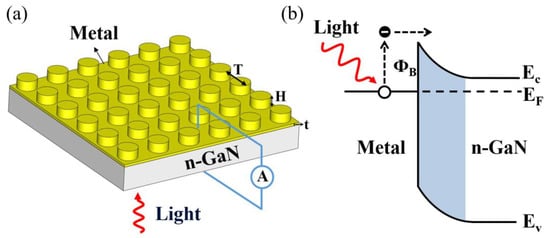
Figure 1.
(a) Schematic of the metal/GaN-nanopillar structure with period T, height H and metal film thickness t. (b) Schematic of the energy band diagram and the detection mechanism of the hot-electron photodetector, the light blue area is the depletion region.
According to the Schottky–Mott relationship, SBH (ΦB) can be written as , where W and Χ are the work function of metal and the electron affinity of semiconductor, respectively [24]. The electron affinity of GaN is 4.1 eV, and Au with a work function of 5.1 eV is used for the preparation of the Schottky contact. Apart from the metal materials, the doping level of GaN has an important impact on the width of the depletion region, which will affect the properties of the Schottky contact. The device based on metal/GaN nanopillars consists of an Ohmic contact and a Schottky contact. The unintentional-doped GaN with a doping density of about 1 × 1016 cm−3 prefers to form a Schottky contact; however, it is difficult to form a good ohmic contact necessary for the collection of the photoncurrent. Therefore, a lightly Si-doped GaN with a doping concentration of 6 × 1017 cm−3 was adopted for the metal/GaN hot-electron photodetector.
The finite-difference time-domain (FDTD) method was carried out to investigate the optical properties of the Au/GaN nanopillars. The periodic boundary conditions were used along the x and y directions, and the perfectly matched layer (PML) conditions were used along the z direction for a single cell. A plane wave with the electric component polarized along the x axis was employed as a stimulation source and was projected normally on the device. Two monitors were used to record the reflection coefficient (R) and transmission coefficient (T) during the simulation, and the absorption coefficient (A) can be obtained as A = 1 − T − R. A significant enhancement on the absorption efficiency in the SWIR range can be expected when utilizing the metal/GaN-nanopillar structures, as shown in Figure 2b. The period of nanopillar array has a great influence on the absorption wavelength, and the absorption peak shifts to longer wavelengths with the increase in the nanopillar period. The period of the Au/GaN-nanopillar arrays in the following experiments was set to 800 nm. The surface plasmons resonance wavelengths can be expressed as for the back-illumination mode [25], where i and j are integers indicating the order of the coupling, and n is the GaN refractive index. The resonance wavelength of the Au/GaN-nanopillar arrays with p = 0.8 μm was calculated to be 1.84 μm, which agrees well with the simulation results in Figure 2b. The height of the nanopillar and the thickness of the gold film had little effect on the absorption efficiency, as presented in Figure 2c,d, respectively. However, if the gold film was too thin, it was not conducive to the formation of a continuous film on the sidewalls of the GaN nanopillars. Therefore, the thickness of the gold film was set to 50 nm, and the height of the nanopillars was set to 200 nm. The calculated absorption efficiency of the Au/GaN-nanopillar structure at the peak wavelength could reach 80%. This is because the Au/GaN-nanopillar arrays can generate surface plasmons that have a local enhancement effect, as illustrated in Figure 2e, and an electric field with a high intensity was observed around the bottom corner of the nanopillar. The simulated Au/GaN-nanopillar arrays had a period of 800 nm and a height of 200 nm, and a 50 nm thick Au is assumed to conformally cover the GaN nanopillar. Figure 2f shows the hot-electron generation rate (G), which is proportional to the electric field intensity in the metal [21]. Hot electrons are mainly generated near the metal/GaN interface, which is in favor of the collection of hot electrons by GaN.
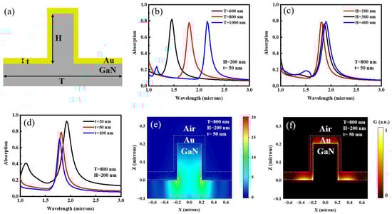
Figure 2.
(a) The parameters of the Au/GaN-nanopillar structure. (b–d) Calculated absorption spectra of the Au/GaN-nanopillar array with a varying period, height, and thickness, respectively. (e) Simulated distributions of the electric field intensity under optical excitation at a wavelength of 1.8 μm. (f) The distribution of the hot-electron generation rate (G) under optical excitation at a wavelength of 1.8 μm.
Figure 3 shows the schematic of the preparation process for the hot-electron photodetectors based on the Au/GaN-nanopillar arrays. First, GaN film was grown on a c-plane sapphire substrate using an AIXTRON 2000HT metal–organic chemical vapor deposition (MOCVD) system. The thickness of the n-GaN film was about 6 μm. A 200 nm thick SiNx was then deposited on the surface of n-GaN by plasma-enhanced chemical vapor deposition (PECVD). A monolayer of polystyrene (PS) spheres was prepared on the SiNx using a self-assembly technique. A non-close-packed PS sphere monolayer was formed by reactive ion etching (RIE) in O2 plasma for a certain time. Then, GaN-nanopillar arrays could be obtained by two-step dry etching, as illustrated in Figure 3d,e, where the PS sphere pattern transferred to the SiNx layer by RIE in SF6, and then through dry-etching of GaN nanopillars using Cl2/BCl3/Ar inductively coupled plasma (ICP). Finally, the Schottky contact and Ohmic contact were prepared sequentially. Utilizing the PS sphere monolayer as an etching mask can achieve a low-cost and large-area fabrication. For comparison measurements, planar structure devices without the GaN nanopillars were also prepared using the same wafer.
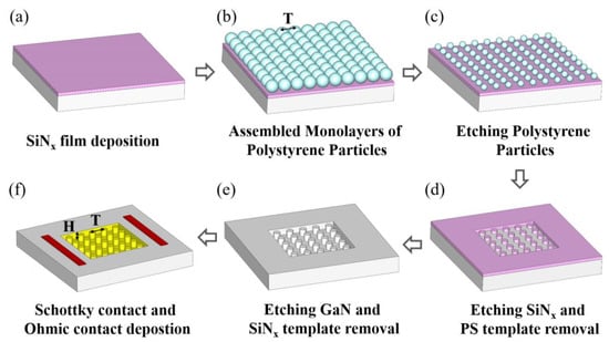
Figure 3.
Schematic diagram of the preparation process for the Au/GaN-nanopillar array-based hot-electron photodetectors; the Au/GaN-nanopillar arrays have a period of T and a height of H. (a) SiNx film was deposited on the surface of n-GaN. (b) Assmbled monolayers of polystyrene particles. (c) A non-close-packed PS sphere monolayer was formed by reactive ion etching. (d) The PS sphere pattern transferred to the SiNx layer by RIE. (e) GaN-nanopillar arrays were obtained by dry etching. (f) The preparation of the Schottky contact and Ohmic contact.
The morphology of the samples was characterized by a scanning electron microscope (SEM, ZEISS Merlin). The optical property measurements were carried out on a Fourier transform infrared spectrometer (Bruker Vertex 80). The measurements of the current-voltage characteristics were performed with an Agilent 4155C parameter analyzer. An 1173 K blackbody with a long-wavelength pass filter (>1.1 μm, Thorlabs) was chosen as the light source for characterizing the photocurrent of the devices. The wavelength-dependent responsivity was measured by illuminating the devices with a tunable laser (NKT Photonics), performing at a wavelength from 1300 to 2100 nm with a step of 25 nm. The photocurrent signal in response to each wavelength was measured using a lock-in amplifier (Stanford Research System SR830) with a 200 Hz chopper.
3. Results
Figure 4a shows the SEM image of the Au/GaN nanopillars, which displays a regular periodic array. A continuous metal film is formed on the surface and sidewall of the nanopillar, as presented in Figure 4b, which is beneficial to the following electrical testing procedure. The Au films in the top and sidewall of the GaN nanopillar had a thickness of 50 nm and 25 nm, respectively. The reflection spectra and transmission spectra were measured using a Fourier transform infrared spectrometer. The reflection spectra and transmission spectra were normalized to a gold mirror and air, respectively. Figure 5a presents the measured reflection (R) and transmission (T) spectra of the planar-type device and the Au/GaN-nanopillar device. The absorption coefficient (A) can be calculated from the reflection coefficient (R) and transmission coefficient (T) as A = 1 − T − R. The optical absorption of the Au/GaN planar-type device and the Au/GaN-nanopillar device is shown in Figure 5b. The absorption efficiency of the Au/GaN-nanopillar structure in the SWIR range is enhanced to over 60%, which is five times higher than the average for the planar structure. In addition, compared with the simulated absorption spectrum in Figure 2b, the measured absorption peak is basically located in the similar wavelength, but widened, which may result from the size fluctuation of the Au/GaN nanopillars.
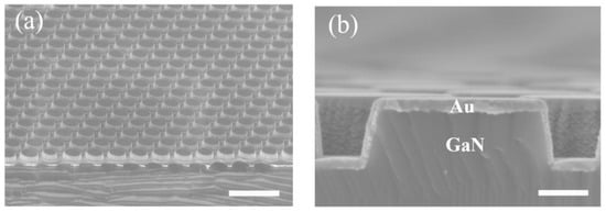
Figure 4.
(a) Typical SEM image of the Au/GaN-nanopillar arrays (scale bar, 2 μm). (b) Cross-section of the Au/GaN nanopillar (scale bar, 200 nm).
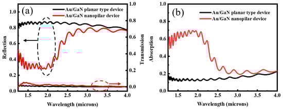
Figure 5.
The measured reflection, transmission (a), and absorption (b) spectra of the Au/GaN planar-type device and the Au/GaN-nanopillar device.
The dry etching process has a significant influence on the n-GaN surface properties. The ICP etching of the n-GaN surface creates high-density N vacancies acting as donors [26,27], which results in the formation of Ohmic-like contacts, as shown in Figure 6a. The current of the Au/GaN-nanopillar device in the voltage range of −1 V~0 V in the absence of incident light is large (blue line in Figure 6a), which is harmful to the photoresponse performance. It is necessary to improve the Schottky contact to reduce the dark current. Therefore, before the metal deposition, the etched GaN nanopillars were annealed in nitrogen ambience to recover the etching damage. As illustrated in Figure 6a, an appropriate annealing temperature, for example 700 °C, is beneficial to improve the rectifying characteristics of the Schottky contact. Figure 6b shows the I–V characteristics for the Au/GaN planar-type device (black line), Au/GaN-nanopillar device without annealing (blue line), and Au/GaN-nanopillar device annealed at 700 °C for 30 s (red line). The rectifying characteristics of Au/GaN became worse after ICP etching, and were partially recovered by rapid-thermal annealing, which can effectively eliminate the etch-induced lattice disorder and point defects [28,29]. Compared with the planar structure (black line in Figure 6b), the rectification effect of the Au/GaN-nanopillar structure is not fully recovered. This is because some dry-etch-induced damage (e.g., point defects) is irreversible.
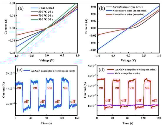
Figure 6.
(a) The I-V curve for the Au contact with the GaN nanopillar as a function of the annealing temperature. (b) The typical I-V characteristics of an Au/GaN planar-type device, Au/GaN-nanopillar device (unannealed), and Au/GaN-nanopillar device (annealed). The current–time curve of the Au/GaN-nanopillar device without annealing (c), annealed Au/GaN-nanopillar device, and GaN-nanopillar device (d) at zero bias.
According to the thermal emission theory [24]
where A is the area of the Schottky contact, A* is the effective Richardson constant, V is the applied voltage, and T is the temperature. The SBHs of the planar-type device, annealed Au/GaN-nanopillar device, and as-etched Au/GaN-nanopillar device can be fitted to be 0.39 eV, 0.19 eV, and ~0 eV, respectively. The ideality factor of the planar-type device and annealed Au/GaN-nanopillar device are 1.6 and 2.2, respectively. It is noteworthy that the SBH was recovered to 0.19 eV from about 0 V after post-etching annealing, but was still much lower than the original value of 0.39 eV.
The photoresponse performance at zero bias of the annealed Au/GaN-nanopillar device and the Au/GaN-nanopillar device without annealing under alternative light illumination from a blackbody with a long-wavelength pass filter (cutoff wavelength of 1.1 μm) are presented in Figure 6c,d, respectively. The photo-to-dark current ratio (PDCR) gives information about the signal-to-noise ratio and can be expressed as follows:
where Ip and Id are the currents measured at the light illumination and in the absence of incident light, respectively. The photocurrent (Ip − Id) of the Au/GaN-nanopillar device without annealing is larger than that of the annealed Au/GaN-nanopillar device, but its dark current (Id) is also larger. As a result, the PDCR of the annealed Au/GaN-nanopillar device (~3.1) is about four times larger than that of the Au/GaN-nanopillar device without annealing (~0.65). The results indicate that annealing is an effective way to improve the detection performance. In order to show whether the IR response is from the defect, the photoresponse of the GaN-nanopillar device was measured, as illustrated in Figure 6d. The GaN-nanopillar device had no response to IR, which suggests the IR response was from the hot-electrons generated in metal, instead of the defect or other factors in GaN.
Figure 7a presents the wavelength-dependent responsivities of the Au/GaN planar-type device and the annealed Au/GaN-nanopillar device. The photoresponse of the annealed Au/GaN-nanopillar device clearly extended beyond 2000 nm, which indicates that the proposed device is capable of detecting light well below the bandgap of GaN. The responsivity ratio is the ratio of the responsivity of the Au/GaN-nanopillar device to the Au/GaN planar-type device, which increases at first and decreases later, as shown in Figure 7b. The responsivity of the Au/GaN-nanopillar device in the SWIR range can be enhanced by about two orders of magnitude, which is mainly attributed to the surface plasmons generated by the Au/GaN-nanopillar device.
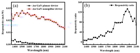
Figure 7.
(a) Responsivity spectra of the Au/GaN-nanopillar device and Au/GaN planar-type device. (b) The responsivity ratio of the Au/GaN-nanopillar device to the Au/GaN planar-type device.
4. Conclusions
In conclusion, we have designed and prepared a hot-electron photodetector-based on a Au/GaN-nanopillar structure, which can operate in the short-wave infrared regime well below the GaN bandgap energy. A suitable SBH has been developed for a higher photo-to-dark current ratio by post-etching annealing. The surface plasmons generated by the Au/GaN-nanopillar arrays can effectively improve the light absorption efficiency. The responsivity of the Au/GaN-nanopillar device in the SWIR range can be enhanced by about two orders of magnitude compared with the planar device. When light enters the Au/GaN-nanopillar device from the substrate, the UV can be absorbed by GaN and the UV detection is based on the interband transitions of electrons in GaN. While the IR can pass through the GaN to the Au/GaN interface and is absorbed by the Au film, the IR detection is based on the hot-electron photodetection. Therefore, the Au/GaN-nanopillar device can achieve UV–IR dual-color photodetection. With the advantages of a simple structure and easy fabrication, the proposed devices have promising potential application in UV–IR dual-color photodetection.
Author Contributions
Conceptualization, Z.H. and Y.L.; methodology, X.T. and Z.H.; software, X.T.; validation, L.W., C.S., B.X., J.W., Y.H. and H.L.; formal analysis, X.T. and Z.H.; investigation, X.T. and Z.H.; resources, L.W., X.W. and J.Y.; data curation, X.T.; writing—original draft preparation, X.T.; writing—review and editing, X.T., Z.H., Y.L. and J.Y.; visualization, X.T.; supervision, Z.H. and Y.L.; project administration, Z.H. and Y.L.; funding acquisition, Z.H. and Y.L. All authors have read and agreed to the published version of the manuscript.
Funding
This research was funded by the National Key R&D Program of China (2017YFA0205800), the National Natural Science Foundation of China (61991443, 61904093, 61975093, 61974080, 61927811, 61822404, and 61875104), the Key Lab Program of BNRist (BNR2019ZS01005), the China Postdoctoral Science Foundation (2019T120090), and the Collaborative Innovation Centre of Solid-State Lighting and Energy-Saving Electronics.
Conflicts of Interest
The authors declare no conflict of interest.
References
- Khan, M.A.; Kuznia, J.N.; Olson, D.T.; Van Hove, J.M.; Blasingame, M.; Reitz, L.F. High-responsivity Photoconductive Ultraviolet Sensors Based on Insulating Single-crystal GaN Epilayers. Appl. Phys. Lett. 1992, 60, 2917–2919. [Google Scholar] [CrossRef]
- Van Hove, J.M.; Hickman, R.; Klaassen, J.J.; Chow, P.P.; Ruden, P.P. Ultraviolet-Sensitive, Visible-Blind GaN Photodiodes Fabricated by Molecular Beam Epitaxy. Appl. Phys. Lett. 1997, 70, 2282–2284. [Google Scholar] [CrossRef]
- Eisenberg, I.; Alpern, H.; Gutkin, V.; Yochelis, S.; Paltiel, Y. Dual Mode UV/Visible-IR Gallium-Nitride Light Detector. Sens. Actuators A Phys. 2015, 233, 26–31. [Google Scholar] [CrossRef]
- Perera, A.G.U.; Ariyawansa, G.; Rinzan, M.B.M.; Stevens, M.; Alevli, M.; Dietz, N.; Matsik, S.G.; Asghar, A.; Ferguson, I.T.; Luo, H.; et al. Performance Improvements of Ultraviolet/Infrared Dual-Band Detectors. Infrared Phys. Technol. 2007, 50, 142–148. [Google Scholar] [CrossRef]
- Perera, A.G.U.; Jayasinghe, R.C.; Ariyawansa, G.; Dietz, N.; Matsik, S.G.; Ferguson, I.T.; Liu, H.C. GaN-Based Heterojunction Structures for Ultraviolet/Infrared Dual-Band Detection. In Proceedings of the 2009 IEEE Nanotechnology Materials and Devices Conference, Traverse City, MI, USA, 2–5 June 2009; pp. 142–147. [Google Scholar]
- Solanke, S.V.; Soman, R.; Rangarajan, M.; Raghavan, S.; Nath, D.N. UV/Near-IR Dual Band Photodetector Based on p-GaN/α-In2Se3 Heterojunction. Sens. Actuators A Phys. 2021, 317, 112455. [Google Scholar] [CrossRef]
- Starikov, D.; Boney, C.; Pillai, R.; Bensaoula, A. Dual-Band UV/IR Optical Sensors for Fire and Flame Detection and Target Recognition. In Proceedings of the ISA/IEEE Sensors for Industry Conference, New Orleans, LA, USA, 27–29 January 2004; pp. 36–40. [Google Scholar]
- Ariyawansa, G.; Rinzan, M.B.M.; Alevli, M.; Strassburg, M.; Dietz, N.; Perera, A.G.U.; Matsik, S.G.; Asghar, A.; Ferguson, I.T.; Luo, H.; et al. GaN/AlGaN Ultraviolet/Infrared Dual-Band Detector. Appl. Phys. Lett. 2006, 89, 091113. [Google Scholar] [CrossRef]
- Hofstetter, D.; Theron, R.; Baumann, E.; Giorgetta, F.R.; Golka, S.; Strasser, G.; Guillot, F.; Monroy, E. Monolithically Integrated AlGaN/GaN/ AlN-Based Solar-Blind Ultraviolet and near-Infrared Detectors. Electron. Lett. 2008, 44, 1–2. [Google Scholar] [CrossRef] [Green Version]
- White, T.P.; Catchpole, K.R. Plasmon-Enhanced Internal Photoemission for Photovoltaics: Theoretical Efficiency Limits. Appl. Phys. Lett. 2012, 101, 073905. [Google Scholar] [CrossRef] [Green Version]
- Knight, M.W.; Sobhani, H.; Nordlander, P.; Halas, N.J. Photodetection with Active Optical Antennas. Science 2011, 332, 702–704. [Google Scholar] [CrossRef]
- Lin, K.-T.; Chen, H.-L.; Lai, Y.-S.; Yu, C.-C. Silicon-Based Broadband Antenna for High Responsivity and Polarization-Insensitive Photodetection at Telecommunication Wavelengths. Nat. Commun. 2014, 5, 3288. [Google Scholar] [CrossRef] [Green Version]
- Gong, T.; Munday, J.N. Materials for Hot Carrier Plasmonics [Invited]. Opt. Mater. Express 2015, 5, 2501. [Google Scholar] [CrossRef]
- Lin, K.-T.; Chan, C.-J.; Lai, Y.-S.; Shiu, L.-T.; Lin, C.-C.; Chen, H.-L. Silicon-Based Embedded Trenches of Active Antennas for High-Responsivity Omnidirectional Photodetection at Telecommunication Wavelengths. ACS Appl. Mater. Interfaces 2019, 11, 3150–3159. [Google Scholar] [CrossRef] [PubMed]
- Qi, Z.; Zhai, Y.; Wen, L.; Wang, Q.; Chen, Q.; Iqbal, S.; Chen, G.; Xu, J.; Tu, Y. Au Nanoparticle-Decorated Silicon Pyramids for Plasmon-Enhanced Hot Electron near-Infrared Photodetection. Nanotechnology 2017, 28, 275202. [Google Scholar] [CrossRef]
- Wen, L.; Chen, Y.; Liang, L.; Chen, Q. Hot Electron Harvesting via Photoelectric Ejection and Photothermal Heat Relaxation in Hotspots-Enriched Plasmonic/Photonic Disordered Nanocomposites. ACS Photonics 2018, 5, 581–591. [Google Scholar] [CrossRef]
- Li, W.; Valentine, J. Metamaterial Perfect Absorber Based Hot Electron Photodetection. Nano Lett. 2014, 14, 3510–3514. [Google Scholar] [CrossRef] [PubMed]
- Yang, Z.; Du, K.; Wang, H.; Lu, F.; Pang, Y.; Wang, J.; Gan, X.; Zhang, W.; Mei, T.; Chua, S.J. Near-Infrared Photodetection with Plasmon-Induced Hot Electrons Using Silicon Nanopillar Array Structure. Nanotechnology 2019, 30, 075204. [Google Scholar] [CrossRef]
- Syu, H.-J.; Chuang, H.-C.; Lin, M.-J.; Cheng, C.-C.; Huang, P.-J.; Lin, C.-F. Ultra-Broadband Photoresponse of Localized Surface Plasmon Resonance from Si-Based Pyramid Structures. Photonics Res. 2019, 7, 1119–1126. [Google Scholar] [CrossRef]
- Barnes, W.L.; Dereux, A.; Ebbesen, T.W. Surface Plasmon Subwavelength Optics. Nature 2003, 424, 824–830. [Google Scholar] [CrossRef]
- Zhang, C.; Cao, G.; Wu, S.; Shao, W.; Giannini, V.; Maier, S.A.; Li, X. Thermodynamic Loss Mechanisms and Strategies for Efficient Hot-Electron Photoconversion. Nano Energy 2019, 55, 164–172. [Google Scholar] [CrossRef]
- Chalabi, H.; Schoen, D.; Brongersma, M.L. Hot-Electron Photodetection with a Plasmonic Nanostripe Antenna. Nano Lett. 2014, 14, 1374–1380. [Google Scholar] [CrossRef]
- Chang, L.; Besteiro, L.V.; Sun, J.; Santiago, E.Y.; Gray, S.K.; Wang, Z.; Govorov, A.O. Electronic Structure of the Plasmons in Metal Nanocrystals: Fundamental Limitations for the Energy Efficiency of Hot Electron Generation. ACS Energy Lett. 2019, 4, 2552–2568. [Google Scholar] [CrossRef]
- Di Bartolomeo, A. Graphene Schottky Diodes: An Experimental Review of the Rectifying Graphene/Semiconductor Heterojunction. Phys. Rep. 2016, 606, 1–58. [Google Scholar] [CrossRef] [Green Version]
- Lee, S.C.; Krishna, S.; Brueck, S.R.J. Light Direction-Dependent Plasmonic Enhancement in Quantum Dot Infrared Photodetectors. Appl. Phys. Lett. 2010, 97, 021112. [Google Scholar] [CrossRef]
- Fan, Q.; Chevtchenko, S.; Ni, X.; Cho, S.-J.; Yun, F.; Morkoç, H. Reactive Ion Etch Damage on GaN and Its Recovery. J. Vac. Sci. Technol. B 2006, 24, 1197. [Google Scholar] [CrossRef]
- Mohammad, S.N. Contact Mechanisms and Design Principles for Alloyed Ohmic Contacts to N-GaN. J. Appl. Phys. 2004, 95, 7940–7953. [Google Scholar] [CrossRef]
- Chen, J.Y.; Pan, C.J.; Chi, G.C. Electrical and Optical Changes in the near Surface of Reactively Ion Etched N-GaN. Solid-State Electron. 1999, 43, 649–652. [Google Scholar] [CrossRef]
- Hong, H.-G.; Kim, S.-S.; Lee, T.; Kim, K.-K.; Song, J.-O. Recovery of Dry Etch-induced Damage of Nano-patterned GaN-based Light-emitting Diodes by Rapid-thermal-annealing. Phys. Status Solidi A 2007, 204, 881–886. [Google Scholar] [CrossRef]
Publisher’s Note: MDPI stays neutral with regard to jurisdictional claims in published maps and institutional affiliations. |
© 2022 by the authors. Licensee MDPI, Basel, Switzerland. This article is an open access article distributed under the terms and conditions of the Creative Commons Attribution (CC BY) license (https://creativecommons.org/licenses/by/4.0/).