Featured Application
Future NIR optoelectronic devices based on 2D materials.
Abstract
Two-dimensional (2D) materials, such as graphene and transition metal dichalcogenides (TMDCs), are highly appealing in the fields of electronics, optoelectronics, energy, etc. Graphene, with high conductivity and high carrier mobility, is an excellent candidate for transparent electrodes. TMDCs have remarkably strong light absorption in the range of visible to infrared wavelength. High-performance photodetectors are expected to achieve through the combination of graphene and TMDCs. Nowadays, near-infrared (NIR) photodetectors play significant roles in many areas. MoTe2 with bandgap energy of about 1.0 eV in its bulk form is a promising material for cost-saving NIR photodetectors. Thus far, only a few of the reported studies on NIR photodetectors built on MoTe2/graphene heterostructures have achieved high responsivity and short response time simultaneously in one device. In this study, we fabricate graphene–MoTe2–graphene vertical van der Waals heterostructure devices through chemical vapor deposition (CVD) growth, wet transfer method, and dry etching technique. Under 1064 nm laser illumination, we acquire responsivity of as high as 635 A/W and a response time of as short as 19 μs from the as-fabricated device. Moreover, we acquire higher responsivity of 1752 A/W and a shorter response time of 16 μs from the Al2O3-encapsulated device. Our research drives the application of 2D materials in the NIR wavelength range.
1. Introduction
Over the years, two-dimensional (2D) materials, such as graphene and transition metal dichalcogenides (TMDCs), have stimulated great research enthusiasm in the fields of electronics, optoelectronics, energy, etc. [1]. In addition to having ultrahigh carrier mobility, low resistance, and near-perfect optical transparency, graphene can also form clean interfaces with other 2D materials, so it can serve as an excellent electrode for photodetectors [2,3]. Transition metal dichalcogenides (TMDCs), which have remarkably strong light absorption in the wavelength range from visible to infrared, are promising candidates for broadband optical detection [3,4].
Nowadays, near-infrared (NIR) photodetectors play significant roles in areas such as telecommunication, remote sensing, and biomedical imaging. However, commercialized NIR photodetectors have high costs of preparation and require harsh operating environments. These factors limit their application. Therefore, there is an urgent need for alternative materials that possess high absorption in the NIR region in ambient conditions and can be prepared through cost-saving approaches [5,6,7]. MoTe2, a newly explored TMDC, with bandgap energy of about 1.0 eV in its bulk form, meets the above requirements for NIR photodetectors [3,4,8].
To date, there have been several studies reported about NIR photodetectors based on MoTe2/graphene heterostructures [1,2,3,8,9,10]. The highest responsivity and shortest response time were 970.82 A/W [3] and 6.15 μs [2], respectively, under 1064 nm illumination. Nevertheless, few of these studies achieve high responsivity and fast response speed simultaneously [2,8]. Moreover, the MoTe2 flakes prepared by mechanical exfoliation were used in all these studies, which hampers their large-scale application.
In this study, we fabricate graphene–MoTe2–graphene vertical van der Waals (vdWs) heterostructure devices. Both the graphene and few-layer MoTe2 were grown via the chemical vapor deposition (CVD) method. The devices were constructed using the wet transfer method together with the dry etching technique. The as-fabricated device has an overall high performance with both high responsivity (635 A/W) and short response time (19 μs) under 1064 nm laser illumination. Moreover, we acquire higher responsivity of 1752 A/W and a shorter response time of 16 μs from the Al2O3-encapsulated device. Our research promotes the development of future NIR optoelectronics applications based on 2D materials.
2. Materials and Methods
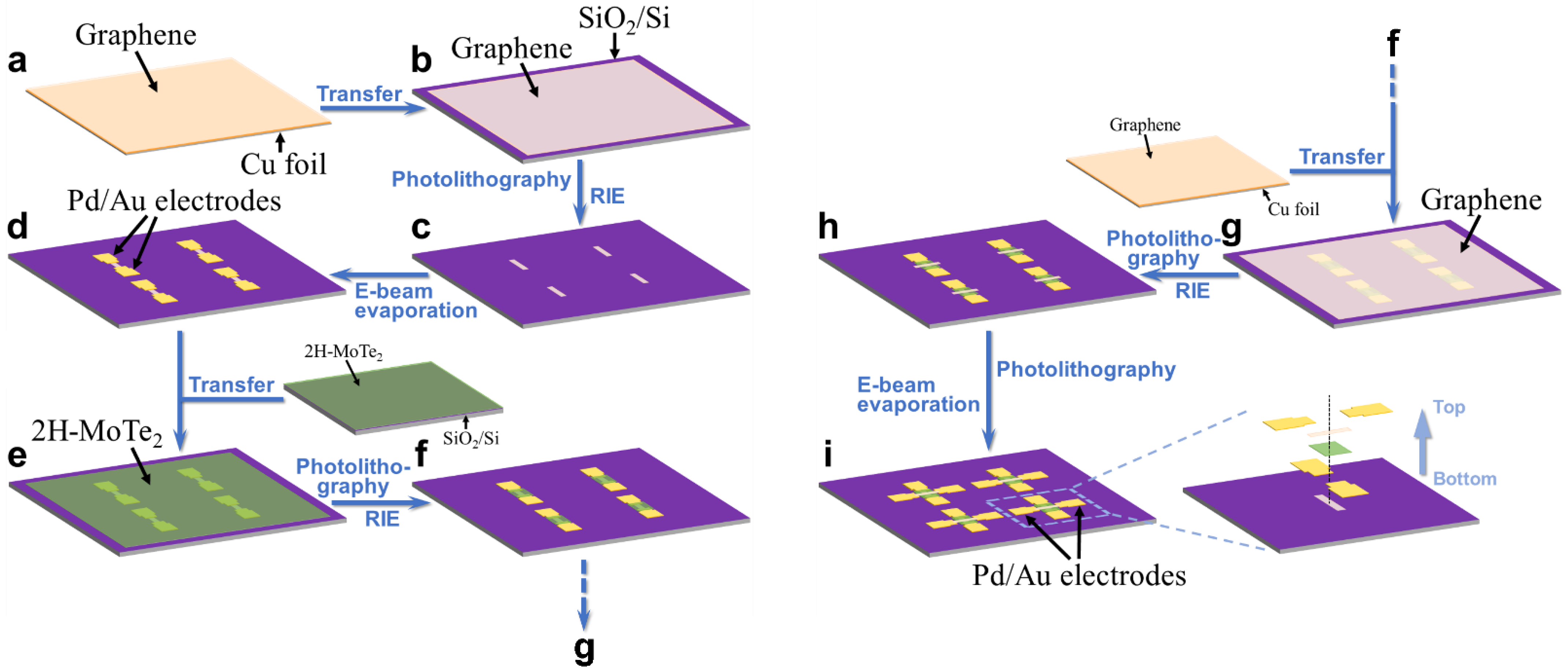
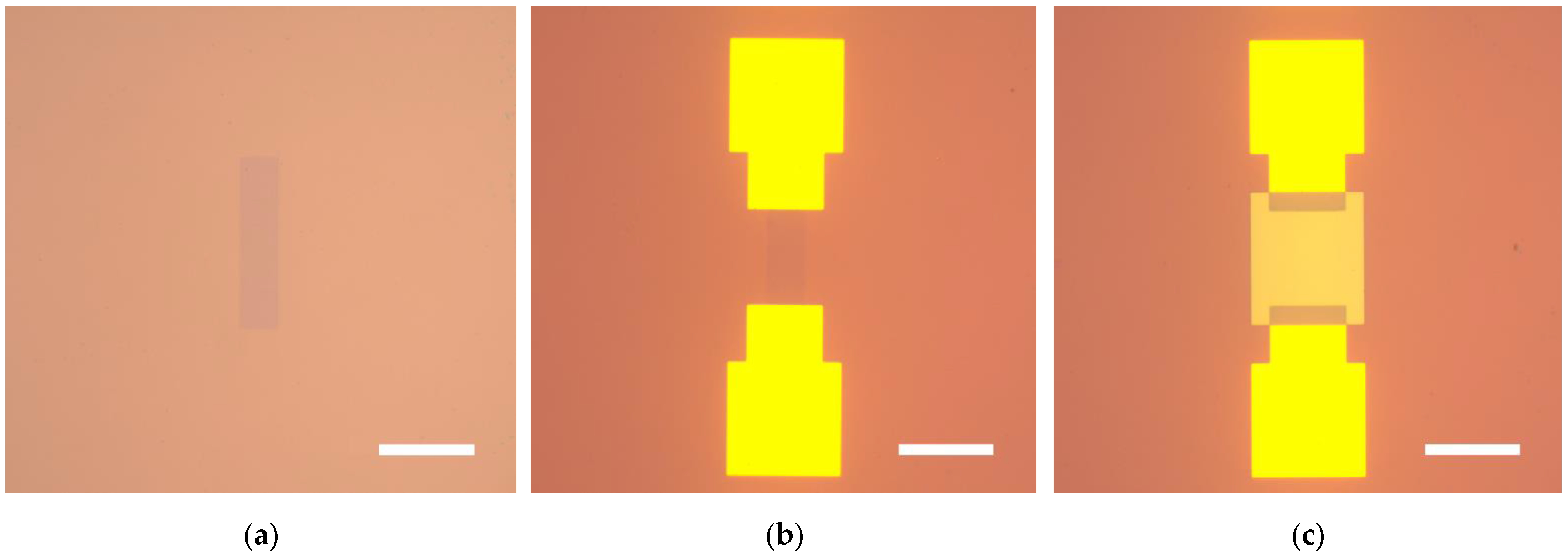
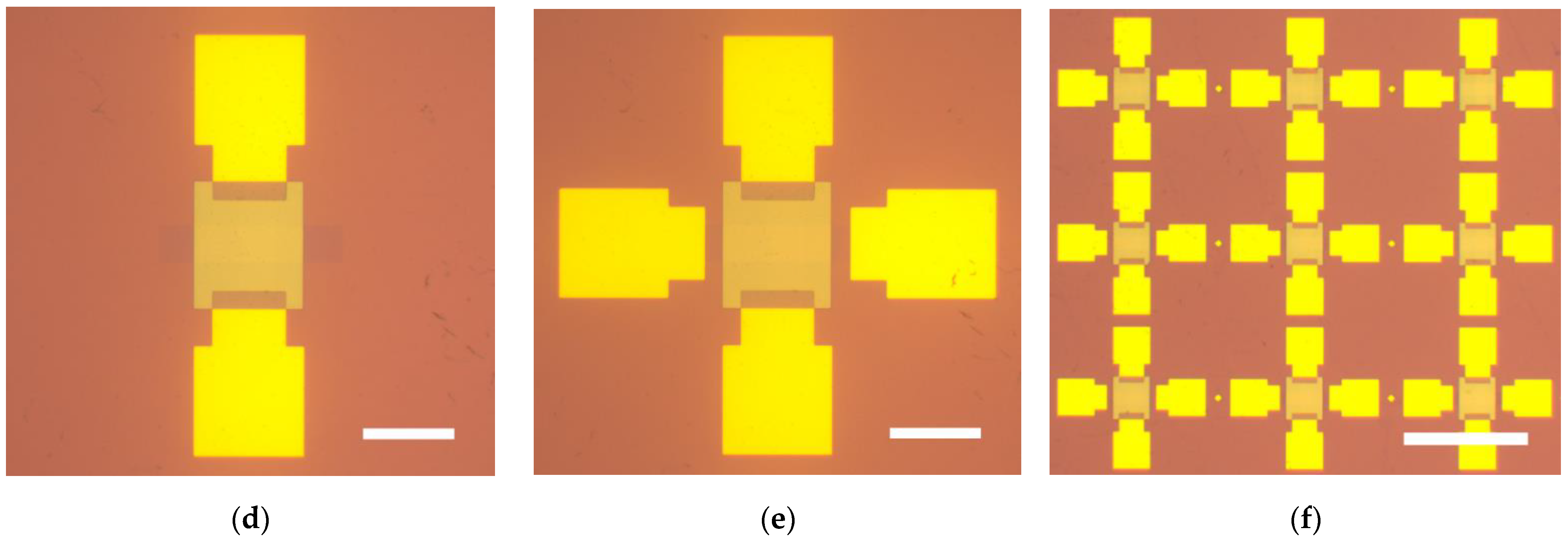
2.1. Fabrication of the Vertical vdWs Heterostructures
The bottom graphene film was grown on Cu foil through the CVD method [11] and transferred from Cu foil to a 285 nm SiO2/p+-Si substrate with the help of polymethyl methacrylate (PMMA) and (NH4)2S2O8 aqueous solution (100 g/L). Then, the graphene film was patterned into a striped array through ultraviolet (UV) lithography and reactive ion etching (RIE). Next, Pd/Au (10/50 nm) electrodes were fabricated on the graphene array through UV lithography, electron beam evaporation, and the lift-off process for measurement purposes. After that, a CVD-grown MoTe2 film [12] was transferred onto the graphene array with the help of PMMA and deionized water. Notably, in this step, we did not use hydrofluoric acid, which was commonly used in previous research [13]. Later, the MoTe2 film was patterned to totally cover the bottom graphene electrodes through UV lithography and RIE. Finally, the top striped graphene electrode array and corresponding Pd/Au electrodes were fabricated in the same way as the bottom ones. Here, the top graphene array was perpendicular to the bottom graphene array.
2.2. Atomic Layer Deposition (ALD) of Al2O3
The Al2O3 that covered the device array was deposited using a Savannah 100 ALD system (Cambridge NanoTech Inc. (Cambridge, MA, USA), Savannah-100). Trimethylaluminum and deionized water served as precursors and N2 served as carrier gas. The reaction temperature was 200 °C. The reaction time was set to achieve an Al2O3 thickness of 20 nm.
2.3. Characterizations
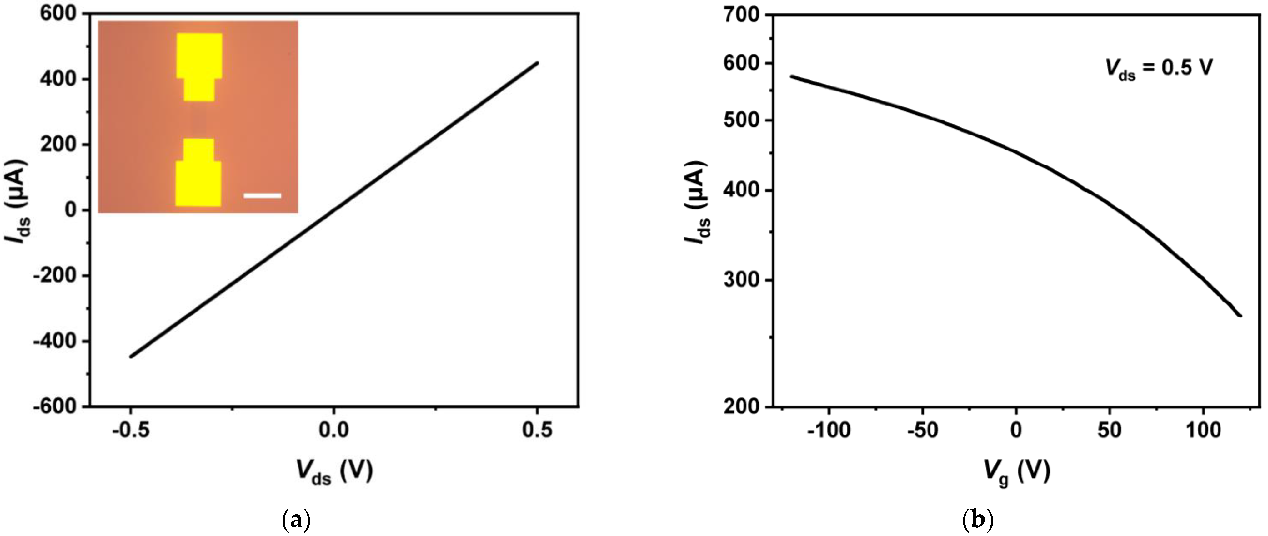
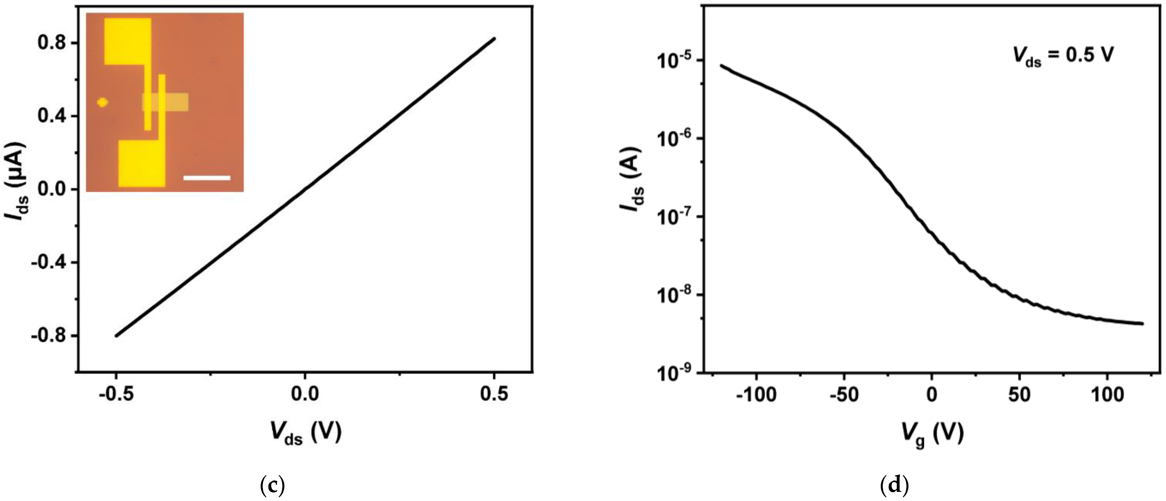
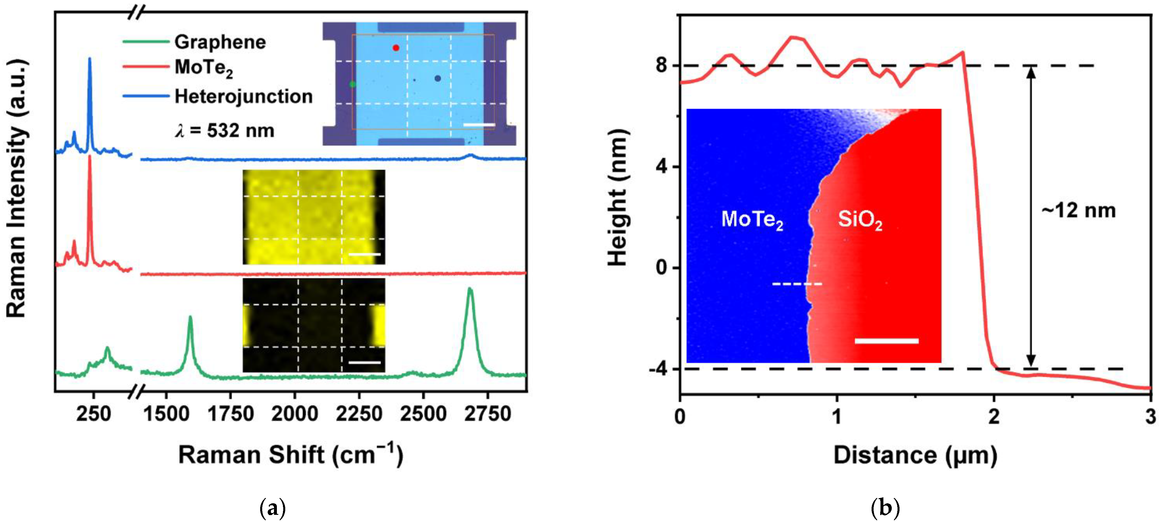
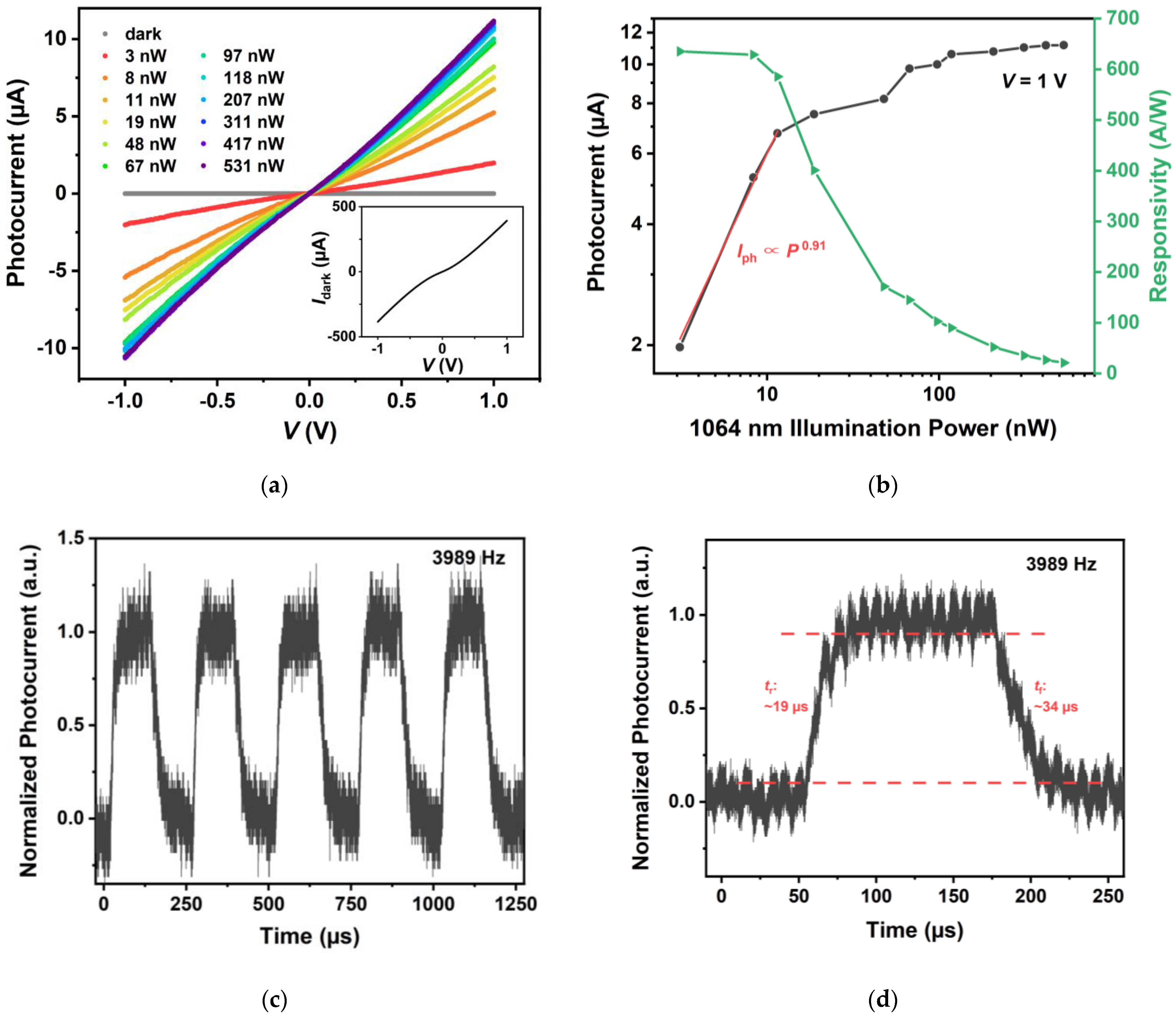
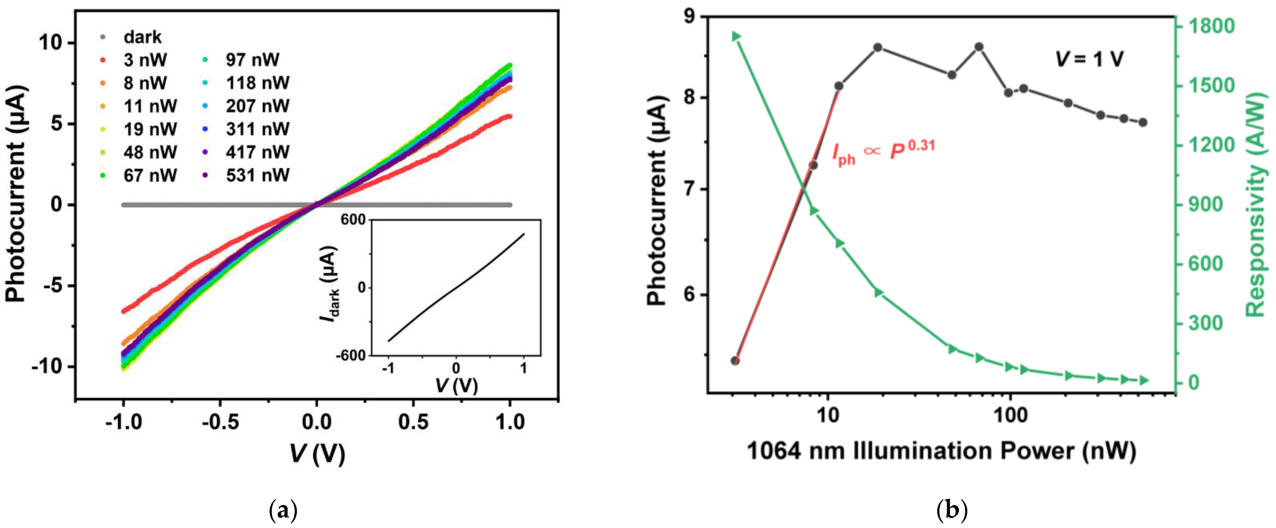
The optical images were taken using an optical microscope (ZEISS (Oberkochen, Germany), Axio Imager A2m). The Raman spectra were collected with a micro-zone confocal Raman system (WITec alpha 300R) under 532 nm laser illumination. The thickness of the MoTe2 film was measured using an atomic force microscope (Asylum Research (Abingdon, UK), Cypher S). All the electrical measurement was conducted in a probe station that was connected to a semiconductor characterization system (Keithley 4200-SCS). For the NIR photoresponse measurement, the 1064 nm laser was introduced to the probe station through a multimode optical fiber with normal incidence. The laser beam is 2.4 mm in diameter. A mechanical chopper, a fixed resistor (5 kΩ), and a digital phosphor oscilloscope (Tektronix DPO 2024) were employed to characterize the temporal photoresponse performance. All the characterizations were performed at room temperature in ambient conditions.
3. Results
Figure 1 illustrates the fabrication procedures of the graphene–MoTe2–graphene vertical vdWs heterostructure array. Figure 2a–e show the optical images taken after each main fabrication step. Figure 2f is the optical image of the heterostructure array, which demonstrates the feasibility of our large-scale fabrication method.
Figure 1.
The fabrication procedures of the Graphene–MoTe2–Graphene vertical vdWs heterostructure array.

Figure 2.
The optical images taken after each main fabrication step: (a) the striped bottom graphene; (b) the graphene with Pd/Au electrodes fabricated on two ends of it for measurement purposes; (c) the optical image taken after the MoTe2 film was transferred and patterned onto the bottom graphene. Herein, the rectangular MoTe2 was designed to completely cover the exposed bottom graphene in order to prevent it from the subsequent etching and the short circuit with the top graphene; (d) another graphene film was transferred onto the top of the MoTe2 and etched into striped shape that was perpendicular to the bottom graphene; (e) finally, the Pd/Au electrodes contacting the top graphene were fabricated. In the vertical heterostructure, the bottom and top graphene layers act as electrodes, and the MoTe2 sheet in between serves as light absorption layer; (f) the graphene–MoTe2–graphene vertical vdWs heterostructure array, which demonstrates the feasibility of our large-scale fabrication method. The scale bar in (a–e) is 100 μm. The scale bar in (f) is 400 μm.
We first characterized the electrical properties of the graphene and MoTe2 films by fabricating graphene and MoTe2 field-effect transistors (FETs), as shown in the insets of Figure 3a,b, respectively. The FETs were fabricated on 285 nm SiO2/p+-Si substrates with Pd/Au (10/50 nm) source and drain electrodes made on two ends of the channel. The p+-Si was used as the back gate. Figure 3a,b show the source–drain current–voltage (Ids–Vds) curve and transfer curve of the graphene FET, respectively. The Ids–Vds curve shows linear behavior, indicating the ohmic contact between the graphene and the Pd/Au electrodes. The transfer curve exhibits p-type behavior. Figure 3c,d show the Ids–Vds curve and transfer curve of the MoTe2 FET, respectively. The transfer curve also exhibits p-type behavior with good ohmic contact between the MoTe2 and the Pd/Au electrodes.

Figure 3.
The optical and electrical characterizations of the graphene and MoTe2 field-effect transistors (FETs): (a) the source-drain current-voltage (Ids–Vds) curve of a graphene FET. Inset: the optical image of the graphene FET. The scale bar is 100 μm. The Ids–Vds curve shows linear behavior, indicating the ohmic contact between the graphene and the Pd/Au electrodes; (b) the transfer curve of the graphene FET, which exhibits p-type behavior; (c) the Ids–Vds curve of a MoTe2 FET. Inset: the optical image of the MoTe2 FET. The scale bar is 100 μm. The Ids–Vds curve shows linear behavior, indicating the ohmic contact between the MoTe2 and the Pd/Au electrodes; (d) the transfer curve of the MoTe2 FET, which exhibits p-type behavior.
Figure 4a shows the Raman spectra measured at graphene, MoTe2, and their heterostructure regions, labeled by the green, red, and blue dots, respectively, of a representative device (the upper inset in Figure 4a). The white dashed lines delineate the outlines of the bottom (vertical) and top (level) graphene. The light-blue area is MoTe2. The Raman spectrum of MoTe2 shows a maximum at 234 cm−1, which is the Raman characteristic peak of 2H-MoTe2 [14]. The Raman spectrum of graphene consists of the Raman characteristic peaks of graphene at 1593 cm−1 and 2681 cm−1 [2,3,15]. In the heterostructure region, the Raman spectrum shows Raman characteristic peaks of both graphene and MoTe2. The middle and lower insets in Figure 4a show the Raman mapping images acquired at 234 cm−1 and 2681 cm−1, respectively, taken in the area labeled by the orange box in the upper inset. It is generally observed that both the overlapping and non-overlapping regions are uniform. Meanwhile, the Raman intensity of the overlapping region is much (slightly) lower than that of the non-overlapping region for graphene (MoTe2). In the case of MoTe2, both the top and bottom single-layer graphene may slightly prevent the effective collection of the Raman scattering signal from MoTe2. In the case of top graphene, the upper surface of MoTe2 may not be a good reflecting surface for Raman scattering signal collection. In the case of bottom graphene, the 12 nm thick MoTe2 may be too thick to realize the good transmission of weak graphene Raman scattering signal. Figure 4b shows the atomic force microscope (AFM) image of the MoTe2 and the surface height profile along the white dashed line. The thickness of the MoTe2 was about 12 nm.
Figure 4.
The Raman and atomic force microscope (AFM) characterizations of the graphene and MoTe2: (a) the Raman spectra measured at graphene, MoTe2, and their heterostructure regions, labeled by the green, red, and blue dots, respectively, of a representative device (the upper inset). The white dashed lines delineate the outlines of the bottom (vertical) and top (level) graphene. The light-blue area is MoTe2. The Raman spectrum of MoTe2 shows the Raman characteristic peak of 2H-MoTe2 at 234 cm−1. The Raman spectrum of graphene consists of the Raman characteristic peaks of graphene at 1593 cm−1 and 2681 cm−1. In the heterostructure region, the Raman spectrum shows Raman characteristic peaks of both graphene and MoTe2. The middle and lower insets show the Raman mapping images acquired at 234 cm−1 and 2681 cm−1, respectively, taken in the area labeled by the orange box in the upper inset. The scale bar is 30 μm. It is generally observed that both the overlapping and non-overlapping regions are uniform. Meanwhile, the Raman intensity of the overlapping region is much (slightly) lower than that of the non-overlapping region for graphene (MoTe2); (b) the AFM image of the MoTe2 and the surface height profile along the white dashed line. The thickness of the MoTe2 is about 12 nm. The scale bar is 5 μm.
Figure 5a shows the photocurrent (Iph)–voltage (V) curves of a representative heterostructure device (device 1) under 1064 nm laser illumination with different illumination power (P) from 3 nW to 531 nW. The inset in Figure 5a shows the current (I)–V curve of device 1 under dark conditions. Here, the photocurrent is defined as Iph = Ilight − Idark, where Ilight and Idark refer to the currents under light illumination and dark conditions, respectively. The illumination power is calculated by multiplying the power density by the device’s effective area, i.e., the overlapping area (S, 1600 μm2) of the bottom and top graphene electrodes. It is shown that Iph increases linearly with V regardless of illumination power. In addition, for identical bias, Iph increases monotonically with illumination power. The Iph and illumination power relation measured at V = 1 V is shown in Figure 5b (the black line). We can see that Iph increases almost linearly in the lower power range but shows a saturated trend when illumination power is higher. Similar phenomena have also been reported before [1,3,4,8,16]. The possible reasons are the increased recombination rate of photogenerated carriers [16], the reduced number of photogenerated carriers contributing to photoconduction under higher photon flux [16], and the existence of trap states in the device [4,16]. As shown by the fitted curve in Figure 5b, the photocurrent and illumination power present a sublinear relation, which can be expressed as Iph = aPb, where a and b are fitted constants. According to the fitting results, we acquired b = 0.91 ± 0.07 (R2 = 0.997) in lower power range. The b value that is smaller than 1 suggests that the photoconduction gain is influenced by the charge traps in the materials and/or their interfaces [2,4,16,17,18,19]. The device’s responsivity (R) and illumination power relation measured at V = 1 V is shown in Figure 5b (the green line). The responsivity is defined as R = Iph/P [4,20]. As illumination power increases, the responsivity decreases monotonically, which corresponds to the saturated trend of the photocurrent. A maximum responsivity of up to 635 A/W is acquired with 3 nW illumination power. Specific detectivity (D*) is another important parameter for a photodetector, which is used to evaluate the capability of weak light detection. When the shot noise from the dark current is the major source of the total noise, specific detectivity can be expressed as D* = RS1/2/(2eIdark)1/2 [4,20,21], where e is the electron charge. Assuming the shot noise from the dark current is the major noise in our case, the specific detectivity of device 1 was calculated to be 2.26 × 10⁹ Jones (cm Hz1/2 W−1) at V = 1 V and 3 nW illumination power. However, it is worth mentioning that, besides shot noise, flicker noise may be of some importance in MoTe2-based devices [22]. Apart from responsivity and specific detectivity, response time is also an important parameter for a photodetector. Figure 5c shows the normalized photocurrent waveform under chopped 1064 nm laser illumination. With a chopping frequency of 3989 Hz, the device presented a stable and repeatable photocurrent response. The rise (fall) time tr (tf) is defined as the time needed for photocurrent to rise (fall) from 10% (90%) to 90% (10%) of the maximum photocurrent in a single response cycle [16,23,24,25]. A rise (fall) time of 19 μs (34 μs) can be acquired from Figure 5d. It is worth noting that, considering the intrinsic response time of the mechanical chopping process (~10 μs) [8], the real response and recovery time of the device should be even shorter.
Figure 5.
The photoresponse performance of device 1: (a) the photocurrent (Iph)–voltage (V) curves under 1064 nm laser illumination with different illumination power (P) from 3 nW to 531 nW. Inset: The current (I)–V curve under dark conditions; (b) the Iph and illumination power relation (the black line), and the responsivity (R) and illumination power relation (the green line) measured at V = 1 V. The red line is the fitted curve with the equation Iph = aPb, where a and b are fitted constants; (c) the normalized photocurrent waveform under chopped 1064 nm laser illumination. The chopping frequency is 3989 Hz; (d) a single normalized response cycle. The rise (fall) time tr (tf) of 19 μs (34 μs) is acquired.
In an attempt to improve the device performance, we deposited a 20 nm thick Al2O3 layer on the as-fabricated devices via the ALD method to protect the devices from ambient. Figure 6a,b show the responsivity-related curves of an encapsulated device (device 2). Similarly, Iph shows a saturated trend when illumination power gets higher (the black line in Figure 6b). Moreover, as illumination power increases, the responsivity decreases monotonically (the green line in Figure 6b). Notably, we obtained an ultrahigh responsivity of up to 1752 A/W at 3 nW illumination power. Meanwhile, assuming the shot noise from the dark current is the major noise, the specific detectivity of device 2 was calculated to be 5.68 × 10⁹ Jones (cm Hz1/2 W−1) at V = 1 V and 3 nW illumination power. The higher responsivity of device 2 in the lower power range may owe to a passivation effect on the surface state-related recombination centers brought by the Al2O3 layer [20,26,27,28], which consequently reduced the recombination of photogenerated carriers and results in enhanced responsivity. According to the fitting results for Iph and illumination power relation, we obtained b = 0.31 ± 0.02 (R2 = 0.998) in the lower power range. The smaller b value indicates that the trap states play a larger role in the photoconduction gain [29]. Figure 6c,d show the temporal photoresponse performance of the device. The device presented a stable and repeatable photocurrent response under light illumination, with a chopping frequency of 3984 Hz and underestimated rise (fall) time of 16 μs (42 μs).

Figure 6.
The photoresponse performance of an Al2O3 (20 nm thick)-encapsulated vertical heterostructure device (device 2): (a) the Iph–V curves under 1064 nm laser illumination with different illumination power from 3 nW to 531 nW. Inset: The I–V curve under dark conditions; (b) the Iph and illumination power relation (the black line), and the responsivity and illumination power relation (the green line) measured at V = 1 V. The red line is the fitted curve with the equation Iph = aPb, where a and b are fitted constants; (c) the normalized photocurrent waveform under chopped 1064 nm laser illumination. The chopping frequency is 3984 Hz; (d) a single normalized response cycle. The tr (tf) of 16 μs (42 μs) is acquired.
Table 1 lists the main performance parameters and corresponding measuring conditions of some reported NIR photodetectors that have similar structures. The maximum responsivity and the response time of our devices are comparable to the best parameters shown in Table 1. Moreover, our devices have higher responsivity and shorter response time simultaneously, whereas only a few other studies have achieved that [2,8]. In our previous research [8], we employed the mechanically exfoliated n-type MoTe2, which formed Schottky contact with p-type graphene. Therefore, the photodetector worked in a photovoltaic mechanism. In this study, we employed the CVD-grown p-type MoTe2. The photodetector works in a photoconductive mechanism. The high responsivity and high speed of our heterostructure devices are because of the excellent optical and electrical properties of graphene and MoTe2, as well as the vertical channel of the heterostructure. Compared with photodetectors that have lateral channels, the vertical heterostructure guarantees a large photosensitive area, together with a shorter carrier transit path. Thus, the vertical heterostructure can overcome the common trade-off between high responsivity and high speed of photodetectors. It is worth noting that even higher responsivity can be expected in our vertical heterostructure devices if we use lower incident illumination power, apply larger V, or enlarge the effective photosensitive area. In addition, our vertical heterostructure devices have low energy consumption in view of the ultrahigh responsivity acquired at the low V (no more than 1 V) and low illumination power (as low as several nanowatts). Moreover, in this study, we demonstrated a practical approach to fabricating photodetector arrays using large-area CVD-grown MoTe2 and graphene, showing the application potential of our devices in integrated circuits.
Table 1.
Comparison of our graphene–MoTe2—graphene vertical vdWs heterostructure photodetectors and other MoTe2-based NIR photodetectors in the literature.
4. Conclusions
In conclusion, we fabricated graphene–MoTe2–graphene vertical vdWs heterostructure devices through CVD growth, wet transfer method, and dry etching technique. Under 1064 nm laser illumination, the responsivity of as high as 635 A/W and response time of as short as 19 μs were obtained from the as-fabricated device. Moreover, we acquired higher responsivity of 1752 A/W and a shorter response time of 16 μs from the Al2O3-encapsulated device. Both the responsivity and response time are comparable to the best results reported in relevant research (Table 1). We attributed the overall high performance of our devices to the merits of both graphene and TMDCs materials and the novel vertical device structure, which guarantees the large photosensitive area and the short carrier transit channel. Our research promotes the development of future NIR optoelectronics applications based on 2D materials.
Author Contributions
Conceptualization, L.D. and W.D.; methodology, L.D., W.D., X.C. and X.X.; validation, L.D. and W.D.; formal analysis, L.D. and W.D.; investigation, W.D. and X.C.; resources, W.D., Z.Z., Z.C., W.X., Y.L. and K.L.; data curation, W.D. and L.D.; writing—original draft preparation, W.D.; writing—review and editing, L.D.; visualization, W.D. and L.D.; supervision, L.D.; project administration, L.D.; funding acquisition, L.D. and K.L. All authors have read and agreed to the published version of the manuscript.
Funding
This study was supported by the National Natural Science Foundation of China (Nos. 61521004, 61874003, 62174005, 92163206, and 51991342).
Institutional Review Board Statement
Not applicable.
Informed Consent Statement
Not applicable.
Data Availability Statement
The data presented in this study are available on request from the corresponding author.
Conflicts of Interest
The authors declare no conflict of interest.
References
- Flory, N.; Ma, P.; Salamin, Y.; Emboras, A.; Taniguchi, T.; Watanabe, K.; Leuthold, J.; Novotny, L. Waveguide-integrated van der Waals heterostructure photodetector at telecom wavelengths with high speed and high responsivity. Nat. Nanotechnol. 2020, 15, 118–124. [Google Scholar] [CrossRef] [PubMed]
- Wei, X.; Yan, F.; Lv, Q.; Zhu, W.; Hu, C.; Patane, A.; Wang, K. Enhanced Photoresponse in MoTe2 Photodetectors with Asymmetric Graphene Contacts. Adv. Opt. Mater. 2019, 7, 8. [Google Scholar] [CrossRef] [Green Version]
- Yu, W.; Li, S.; Zhang, Y.; Ma, W.; Sun, T.; Yuan, J.; Fu, K.; Bao, Q. Near-Infrared Photodetectors Based on MoTe2/Graphene Heterostructure with High Responsivity and Flexibility. Small 2017, 13, 8. [Google Scholar] [CrossRef] [PubMed]
- Huang, H.; Wang, J.; Hu, W.; Liao, L.; Wang, P.; Wang, X.; Gong, F.; Chen, Y.; Wu, G.; Luo, W.; et al. Highly sensitive visible to infrared MoTe2 photodetectors enhanced by the photogating effect. Nanotechnology 2016, 27, 445201. [Google Scholar] [CrossRef]
- Xu, Y.; Liu, C.; Guo, C.; Yu, Q.; Guo, W.; Lu, W.; Chen, X.; Wang, L.; Zhang, K. High performance near infrared photodetector based on in-plane black phosphorus p-n homojunction. Nano Energy 2020, 70, 104518. [Google Scholar] [CrossRef]
- Li, Q.; Guo, Y.; Liu, Y. Exploration of Near-Infrared Organic Photodetectors. Chem. Mater. 2019, 31, 6359–6379. [Google Scholar] [CrossRef]
- Wang, F.; Zhang, Y.; Gao, Y.; Luo, P.; Su, J.; Han, W.; Liu, K.; Li, H.; Zhai, T. 2D Metal Chalcogenides for IR Photodetection. Small 2019, 15, e1901347. [Google Scholar] [CrossRef]
- Zhang, K.; Fang, X.; Wang, Y.; Wan, Y.; Song, Q.; Zhai, W.; Li, Y.; Ran, G.; Ye, Y.; Dai, L. Ultrasensitive Near-Infrared Photodetectors Based on a Graphene-MoTe2-Graphene Vertical van der Waals Heterostructure. ACS Appl. Mater. Interfaces 2017, 9, 5392–5398. [Google Scholar] [CrossRef]
- Kim, H.J.; Lee, K.J.; Park, J.; Shin, G.H.; Park, H.; Yu, K.; Choi, S.-Y. Photoconductivity Switching in MoTe2/Graphene Heterostructure by Trap-Assisted Photogating. ACS Appl. Mater. Interfaces 2020, 12, 38563–38569. [Google Scholar] [CrossRef]
- Hu, R.-X.; Ma, X.-L.; An, C.-H.; Liu, J. Visible-to-near-infrared photodetector based on graphene-MoTe2-graphere heterostructure. Chin. Phys. B 2019, 28, 117802. [Google Scholar] [CrossRef]
- Xu, X.; Zhang, Z.; Qiu, L.; Zhuang, J.; Zhang, L.; Wang, H.; Liao, C.; Song, H.; Qiao, R.; Gao, P.; et al. Ultrafast growth of single-crystal graphene assisted by a continuous oxygen supply. Nat. Nanotechnol. 2016, 11, 930–935. [Google Scholar] [CrossRef] [PubMed]
- Du, W.; Jia, X.; Cheng, Z.; Xu, W.; Li, Y.; Dai, L. Low-power-consumption CMOS inverter array based on CVD-grown p-MoTe2 and n-MoS2. iScience 2021, 24, 103491. [Google Scholar] [CrossRef] [PubMed]
- Xu, X.; Liu, S.; Han, B.; Han, Y.; Yuan, K.; Xu, W.; Yao, X.; Li, P.; Yang, S.; Gong, W.; et al. Scaling-up Atomically Thin Coplanar Semiconductor-Metal Circuitry via Phase Engineered Chemical Assembly. Nano Lett. 2019, 19, 6845–6852. [Google Scholar] [CrossRef] [PubMed] [Green Version]
- Xu, X.; Chen, S.; Liu, S.; Cheng, X.; Xu, W.; Li, P.; Wan, Y.; Yang, S.; Gong, W.; Yuan, K.; et al. Millimeter-Scale Single-Crystalline Semiconducting MoTe2 via Solid-to-Solid Phase Transformation. J. Am. Chem. Soc. 2019, 141, 2128–2134. [Google Scholar] [CrossRef] [PubMed]
- Zheng, L.; Cheng, X.; Wang, Z.; Xia, C.; Cao, D.; Shen, L.; Wang, Q.; Yu, Y.; Shen, D. Reversible n-Type Doping of Graphene by H2O-Based Atomic-Layer Deposition and Its Doping Mechanism. J. Phys. Chem. C 2015, 119, 5995–6000. [Google Scholar] [CrossRef]
- Buscema, M.; Groenendijk, D.J.; Blanter, S.I.; Steele, G.A.; van der Zant, H.S.J.; Castellanos-Gomez, A. Fast and Broadband Photoresponse of Few-Layer Black Phosphorus Field-Effect Transistors. Nano Lett. 2014, 14, 3347–3352. [Google Scholar] [CrossRef] [Green Version]
- Ghatak, S.; Pal, A.N.; Ghosh, A. Nature of Electronic States in Atomically Thin MoS2 Field-Effect Transistors. ACS Nano 2011, 5, 7707–7712. [Google Scholar] [CrossRef] [Green Version]
- Lopez-Sanchez, O.; Lembke, D.; Kayci, M.; Radenovic, A.; Kis, A. Ultrasensitive photodetectors based on monolayer MoS2. Nat. Nanotechnol. 2013, 8, 497–501. [Google Scholar] [CrossRef]
- Island, J.; Blanter, S.I.; Buscema, M.; Van Der Zant, H.S.J.; Castellanos-Gomez, A. Gate Controlled Photocurrent Generation Mechanisms in High-Gain In2Se3 Phototransistors. Nano Lett. 2015, 15, 7853–7858. [Google Scholar] [CrossRef] [Green Version]
- Jin, W.; Gao, Z.; Zhou, Y.; Yu, B.; Zhang, H.; Peng, H.; Liu, Z.; Dai, L. Novel graphene-oxide-semiconductor nanowire phototransistors. J. Mater. Chem. C 2014, 2, 1592–1596. [Google Scholar] [CrossRef]
- Hu, P.; Wang, L.; Yoon, M.; Zhang, J.; Feng, W.; Wang, X.; Wen, Z.; Idrobo, J.C.; Miyamoto, Y.; Geohegan, D.B.; et al. Highly Responsive Ultrathin GaS Nanosheet Photodetectors on Rigid and Flexible Substrates. Nano Lett. 2013, 13, 1649–1654. [Google Scholar] [CrossRef] [PubMed]
- Ji, H.; Joo, M.-K.; Yun, Y.; Park, J.-H.; Lee, G.M.; Moon, B.H.; Yi, H.; Suh, D.; Lim, S.C. Suppression of Interfacial Current Fluctuation in MoTe2 Transistors with Different Dielectrics. ACS Appl. Mater. Interfaces 2016, 8, 19092–19099. [Google Scholar] [CrossRef] [PubMed]
- Wei, Y.; Ren, Z.; Zhang, A.; Mao, P.; Li, H.; Zhong, X.; Li, W.; Yang, S.; Wang, J. Hybrid Organic/PbS Quantum Dot Bilayer Photodetector with Low Dark Current and High Detectivity. Adv. Funct. Mater. 2018, 28, 28. [Google Scholar] [CrossRef]
- Khan, A.A.; Azam, M.; Eric, D.; Liang, G.-X.; Yu, Z.-N. Triple cation perovskite doped with the small molecule F4TCNQ for highly efficient stable photodetectors. J. Mater. Chem. C 2020, 8, 2880–2887. [Google Scholar] [CrossRef]
- Liang, Y.; Liang, H.; Xiao, X.; Hark, S. The epitaxial growth of ZnS nanowire arrays and their applications in UV-light detection. J. Mater. Chem. 2012, 22, 1199–1205. [Google Scholar] [CrossRef]
- Jiang, Y.; Zhang, W.; Jie, J.S.; Meng, X.M.; Fan, X.; Lee, S.-T. Photoresponse Properties of CdSe Single-Nanoribbon Photodetectors. Adv. Funct. Mater. 2007, 17, 1795–1800. [Google Scholar] [CrossRef]
- Zou, X.; Xu, J.; Huang, H.; Zhu, Z.; Wang, H.; Li, B.; Liao, L.; Fang, G.; Zhu, Z. A comparative study on top-gated and bottom-gated multilayer MoS2 transistors with gate stacked dielectric of Al2O3/HfO2. Nanotechnology 2018, 29, 245201. [Google Scholar] [CrossRef]
- Bolshakov, P.; Zhao, P.; Azcatl, A.; Hurley, P.K.; Wallace, R.M.; Young, C.D. Improvement in top-gate MoS2 transistor performance due to high quality backside Al2O3 layer. Appl. Phys. Lett. 2017, 111, 032110. [Google Scholar] [CrossRef] [Green Version]
- Kung, S.-C.; van der Veer, W.E.; Yang, F.; Donavan, K.C.; Penner, R.M. 20 μs Photocurrent Response from Lithographically Patterned Nanocrystalline Cadmium Selenide Nanowires. Nano Lett. 2010, 10, 1481–1485. [Google Scholar] [CrossRef]
Publisher’s Note: MDPI stays neutral with regard to jurisdictional claims in published maps and institutional affiliations. |
© 2022 by the authors. Licensee MDPI, Basel, Switzerland. This article is an open access article distributed under the terms and conditions of the Creative Commons Attribution (CC BY) license (https://creativecommons.org/licenses/by/4.0/).