Article

Applying Deep Learning to Construct a Defect Detection System for Ceramic Substrates

1
National Taipei University of Technology, Taipei City 106, Taiwan
2
Taiwan Semiconductor Manufacturing Company, Hsinchu 300, Taiwan
*
Author to whom correspondence should be addressed.
Appl. Sci. 2022, 12(5), 2269; https://doi.org/10.3390/app12052269
Submission received: 7 November 2021 / Revised: 9 February 2022 / Accepted: 15 February 2022 / Published: 22 February 2022
(This article belongs to the Special Issue Artificial Intelligence in Industrial Engineering)

Abstract

:
Under the emerging topic of machine vision technology replacing manual examination, automatic optical inspection (AOI) technology has been adopted for the detection of defects in semi-finished/finished products and is widely used for the defect detection of printed circuit boards (PCB) in electronic industries where surface mount technology (SMT) is applied. In order to convert images from gray-scale to binary in the PCB process, a strict threshold value was set for AOI to prevent ‘escapes’, but this can lead to serious false alarm because of unwanted noises. Therefore, they tend to set up a Noise-Removal procedure after AOI, which increases the computational cost. By applying deep learning to circuit images of the ceramic substrates in AOI, this paper aimed to construct an automatic defect detection system that could also identify the categories as well as the locations of defects. This study proposed and evaluated three models with integrated structures: ResNeXt+YOLO v3, Inception v3+YOLO v3, and YOLO v3. The outcomes indicate that the defect detection system built on ResNeXt+YOLO v3 could most effectively detect standard images that had been misidentified as defects by AOI, categorize genuine defects, and find their location. The proposed method could not only increase the inspection accuracy to 99.2%, but also help decrease the cost of human resources generated by manual re-examination.

1. Introduction

The topic of machine vision technology replacing manual examination has recently emerged. This system utilizes digital sensors in an industrial camera to collect images, processes the images via computer software, and then makes decisions after analyzing and measuring various features. Such systems are composed of a console computer, an image capture card, image processors, video camera lighting sources, and a visual display terminal. Machine vision systems used for industrial examination also include a PC-based controller, a programmable logic controller (PLC), and institutional and controlling systems such as a servo motor. Software technology includes algorithms for image processing, artificial intelligence, and pattern recognition [1,2,3,4]. In this respect, Hao et al. in [1] proposed a steel surface defect inspection network with advanced object detection approaches. In their model, a deformable convolution enhanced backbone network is designed to extract the complex features of multi-shape defects. Çelik et al. [2] proposed an automated vision-based inspection system to detect the pixel defects on LCD panels. Tout et al. [3] proposed a fully automated vision system to inspect the whole surface of crankshafts, based on the magnetic particle testing technique. They also designed visual inspection system consisting of a stepper motor and multiple cameras to ensure the inspection of the whole surface of the crankshaft in real-time. Adibhatla et al. [4] presented a deep learning algorithm based on the you-only-look-once (YOLO) approach for the quality inspection of printed circuit boards.
With the development of optical videography technology and image processing/recognition technology, machine vision technology can not only be applied to facial recognition on computers or mobile devices, but can also widely replace manual quality examinations in industrial automation. For example, Automatic Optical Inspection (AOI) technology has been adopted for the detection of defects in semi-finished/finished products and is widely used for the defect detection of PCB in the electronic industries where SMT is applied [5,6,7,8,9,10]. Li et al. [5] proposed an effective self-adaption method that collects “exception data” such as the samples with which the Artificial Intelligent (AI) model made mistakes from the automated optical inspection inference edge to the training server, retraining with exceptions on the server and deploying back to the edge. The proposed defect detection system has been verified with real tests that achieved a detection rate of 99.99% with a FAR 20–30% and less than 15 of inspection time on a resolution 7296 × 6000 PCB image. In order to inspect solder joint defects of Integrated Circuit (IC) components on Printed Circuit Boards (PCBs), Wu and Zhang [6] developed an AOI algorithm. They divided solder joint into several subregions as shape features, and its digital features were extracted by the area, mass center, and continuous pixels. To address the problem of the fixed templates, Ye et al. [7] proposed an IC solder joint inspection method by making an attempt to utilize different templates for different IC solder joints. To this aim, they first used a number of qualified solder joint images to construct a dictionary. Then, they formulated the construction of the adaptive template for each IC solder joint as an optimization problem, which is solved by the elastic net. The defects can be inspected by the difference image between the IC solder joint image and its corresponding adaptive template. Tsai and Huang [8] proposed a global fourier image reconstruction method to detect and localize small defects in nonperiodical pattern images. This method is based on the comparison of the whole fourier spectra between the template and the inspection image. The inverse Fourier transform is then applied to reconstruct the test image, where the local anomaly will be restored and the common pattern will be removed as a uniform surface. The proposed method is invariant to translation and illumination, and can detect subtle defects as small as one-pixel wide in a wide variety of nonperiodical patterns found in the electronic industry. Cai et al. [9] proposed a novel cascaded convolutional neural network for Surface-Mount Technology (SMT) solder joint inspection, whose input is the whole SMT solder joint image rather than its features. Their method adaptively determines the regions of interest of the SMT solder joint image via a sliding-window scheme based on one kind of CNN. It utilizes the characteristic of CNN to combine the global and vital local information of the SMT solder joint image to make accurate predictions using a cascaded structure. Ray and Mukherjee [10] proposed a hybrid approach which helps in producing zero- defect PCB by detecting the defects. This approach not only detects the defect, but also classifies and locates the defects. The hybrid approach uses referential and non-referential methods to analyze the PCB and this approach proposed an algorithm which involves image representation, image comparison, and image segmentation.
Moreover, people in the industries tend to set a strict AOI threshold value to convert images from gray-scale to binary in PCB process and prevent underkills. In this regard, many histogram-based methods used a calculated global threshold, and this leads to serious over-screening, causing manual re-examination to still be required after AOI. Sanguannam and Srinonchat [11] used the mean and standard deviation of pixel values to compute the threshold. The adaptive threshold is more commonly used. Abdelhameed et al. in [12] and also Wu and Chen [13] used the Otsu method to calculate the optimum threshold for pre-processed IC images using the bi-modal histogram. Except for one global threshold, Gao et al. in [14] measured the threshold values for each individual pixel against their neighborhood. However, the histogram-based methods cannot work well when other highlighted components are included, such as markings and via-holds.

1.1. Research Motives

The fundamental principle of AOI is to use optical devices to scan and capture PCB images and then compare those images to standard images stored in a database. If the degree of similarity cannot reach a pre-set threshold value, the image will be identified as a defective image. The parameters for AOI include the brightness of the features, the grayscale value, and the area size reflected in the image. Many people in the industry may set a strict threshold value for AOI to prevent ‘escapes’ and reach a high-quality result rate. However, when the threshold value is too strict, or if there is lighting interference from the neighboring parts, AOI can present false alarms or overkill. Liao [15] pointed out that when AOI is used for PCB inspection, the false alarm rate is as high as 70%, which means 70% of the rejects are actually qualified products. In current practice, people tend to conduct manual re-examinations, and every AOI terminal needs up to four people to perform them, resulting in increased human resource costs. Moreover, there can be inconsistencies in terms of the standards for judgment used in manual re-examinations. Aswini et al. [16] proposed the methods of mathematical morphology and bottom-hat filtering to capture the features of defects, in which defects are strengthened by gray-scale processing and then compared to the threshold value to see whether a defect exists. This approach requires a clear definition of a product’s defects to make accurate predictions; however, as defects in the manufacturing process are dynamic and versatile, they often cannot be clearly or completely defined, making this approach not very expandable.

1.2. Research Purpose

This study aimed to set up a defect detection system to accurately distinguish whether defects exist in PCB based on universal standards in the industry, as well as to identify the categories and locations of the defects so that the inspection accuracy can be improved and the false alarm rate can be decreased. During the study, a self-learning system was built based on deep learning methodologies. The system was trained to automatically start the image processing and calculate the parameters required for deductive reasoning in an iterative process. As the parameters could be updated constantly in an iterative process, inspection standards could be established without a complete product defect definition.

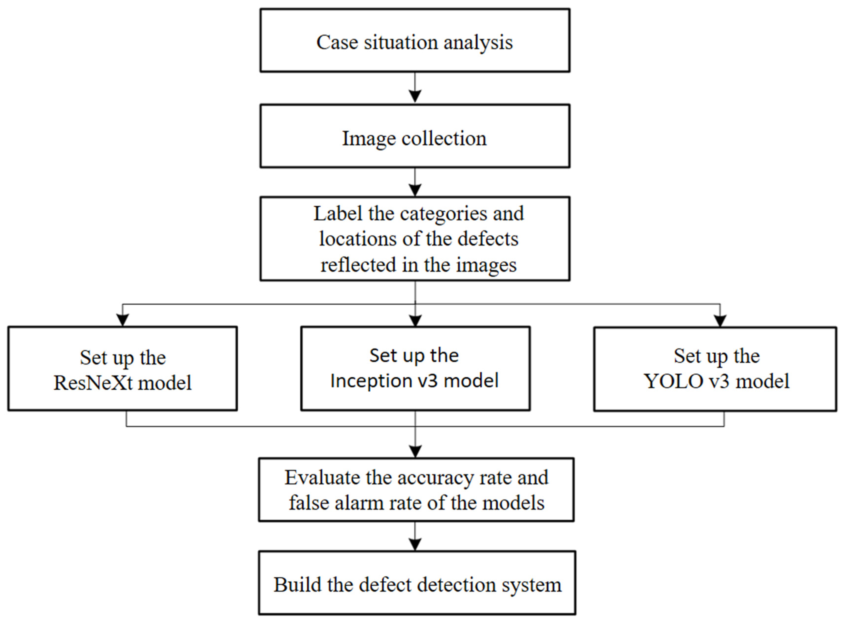
1.3. Research Process

As shown in Figure 1, this study first analyzed the situations of the target products and the AOI terminal. We collected the images produced by the AOI terminal and used them as the training samples for the model. Next, we named the folders, stored the standard images respectively, and used LabelImg-master software to label the categories and locations of the defects. We imported the images into the ResNeXt model and the Inception v3 model respectively to tell whether they were defect or standard images, and then imported the images into the YOLO v3 model to identify their defect categories and locations. We integrated the ResNeXt+YOLO v3 model and the ResNeXt+YOLO v3 model and ran the tests respectively, and then used a confusion matrix to compare the accuracy and false alarm rates. Finally, we chose the one with a higher accuracy rate and a lower false alarm rate as the base model to set up the defect detection system.

2. Materials and Methods

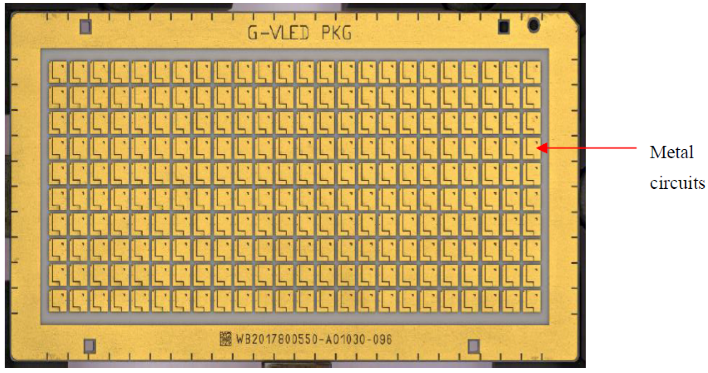
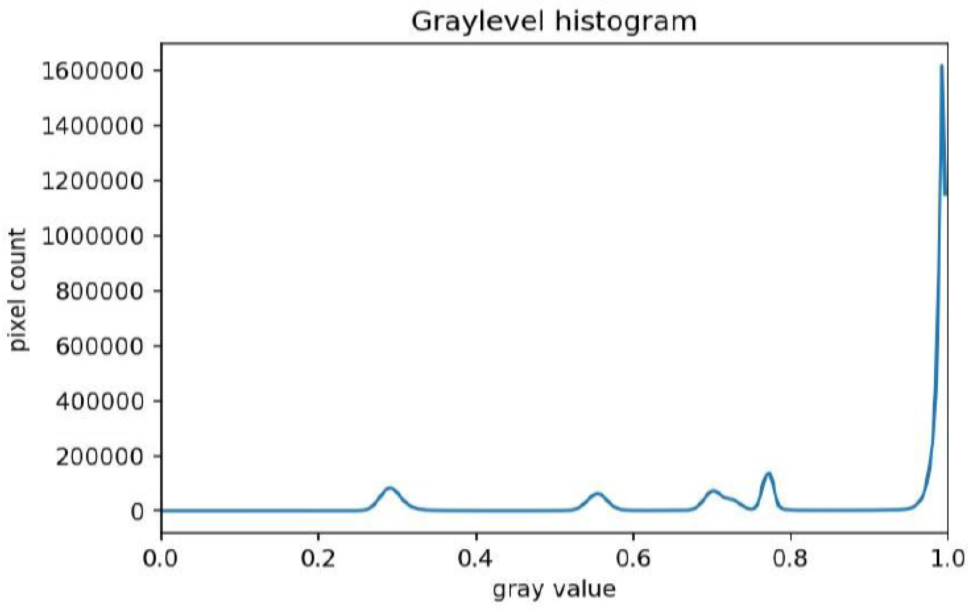
2.1. Case Situation Analysis

This study used a professionally manufactured ceramic substrate as an example. As shown in Figure 2, it was a 24 × 10 array structure and had a circuit pattern imprinted on it. The metal circuits were linked with the ceramic substrate by electric plating, which could make the locations of the circuits be more precise and allow the space between circuits to be narrower. This technique is largely used in industries such as high-power LED and semi-conductor manufacturing. The ceramic substrate joint images are collected by the AOI terminal. The system consists of a charge-coupled device (CCD) digital camera (TAIYO TY-VISION A400 model) and a three-color (red, green, and blue) hemispherical light-emitting diode array light resource.
We converted every gray scale image into a binary image by choosing a predefined threshold (T) in the original image, and then converting every pixel black or white according to whether its gray value is greater than or less than T. Grayscale images contain pixel values in the range from 0 to 1. One way to determine a “good” value for T is to look at the grayscale histogram of the image (Figure 3). Because ceramics have a continuous surface, most of the pixels in the image are bright. Since we wanted to examine the defects of ceramic substrates, we wanted to turn off the healthy pixels, while leaving the pixels for the defects turned on. Thus, we had to choose a value of T somewhere before the large peak and turn pixels above that value “off”. We set the threshold to 0.8. Thus, we used the less operator ≤ to compare the blurred image to the threshold T. Therefore,
  • A pixel turns on, if its gray level is >0.8.
  • A pixel turns off, if its gray level is ≤0.8.
Manufacturers use AOI devices to examine the defects of ceramic substrates and then manually conduct a re-examination. Overkilled ceramic substrates will be returned to the production line for further processing, and ones with genuine defects will be labeled as such. The defect detection rate of AOI is about 20% (Equation (1)), and after the manual re-examination, 15% of the detected defects are found to be false alarms (images that are actually standard).
AOI   Defect   detection   rate = Number   of   ceramic   substrates   detected   as   defected   by   AOI Total   number   of   ceramic   substrates

2.1.1. Image Collection

The quality of the AOI images collected for training the model was largely related to the model’s self-learning and defect detection abilities as well as the model of the video camera, the shooting angle, the scanning speed, the focal length, and the magnification, etc. In this study, the AOI acquisition parameters were a line scan camera with 7500 pixels, the illuminance of 65,100 lux, and the scanning speed of 50 mm/s, respectively. There is a total of 1000 images including standard products and defects for training, validation and testing.

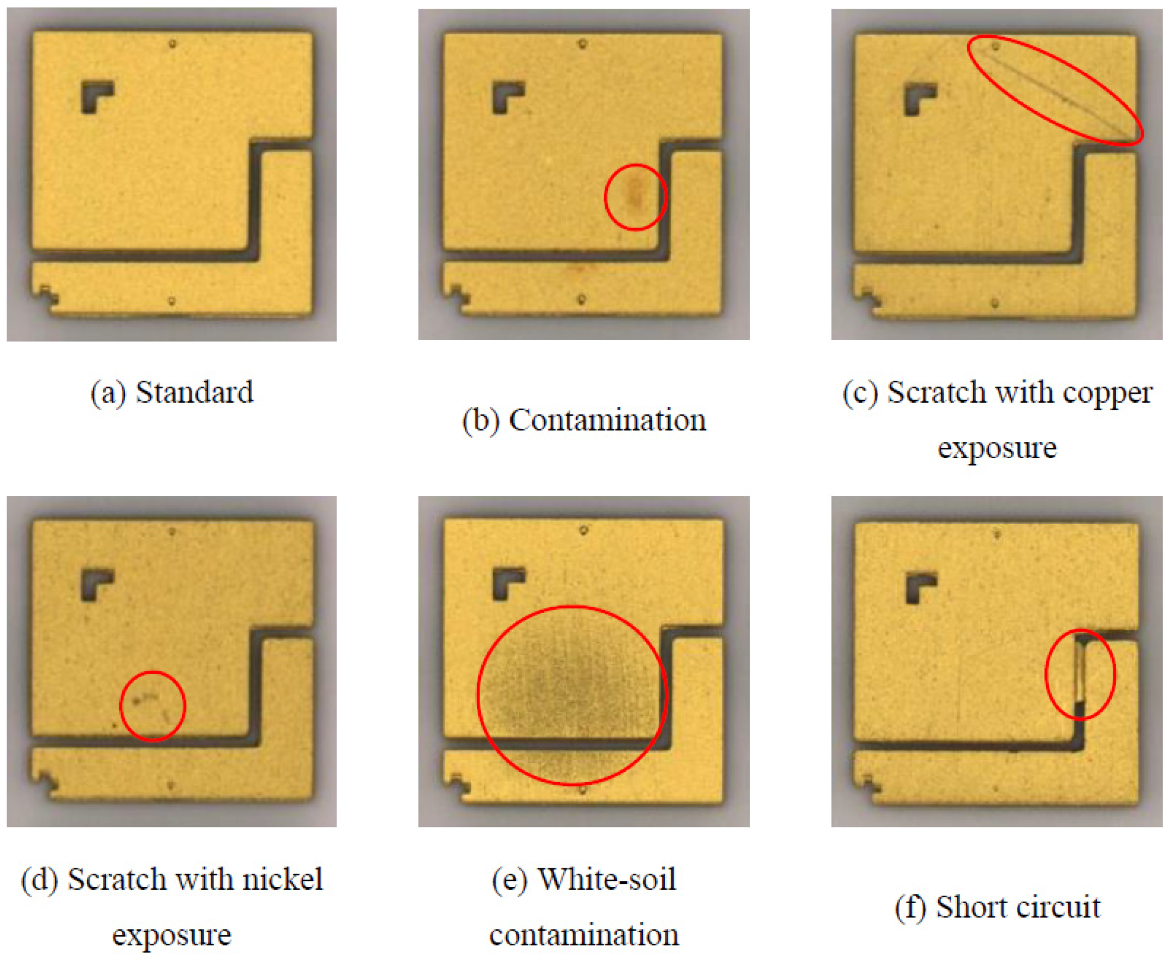
2.1.2. Image Labeling

In this study, discrete components were used as the learning samples for the model. The sample images of standard and all types of defects were labeled based on universal standards in the industry and shown in Figure 4 with explanations. Given that the main defect types were contamination and scratches in this case, this study built the model for these two types of defects. There are 100 images used for test. Among these, 48 images were with defects (24 images were with pollution and the other 24 images were with scratches); 52 images were standard products. The above arrangement of sample images was applied to all the three integrated models.
  • Contamination: Contamination was mostly due to foreign matter from the surrounding environment attaching to the products or sticky dark yellow stains in irregular shapes (Figure 4b).
  • Scratches: There were two types of scratches based on the depth of the scratch: scratches that exposed copper are shown in the shape of a thin line in Figure 4c; scratches that exposed nickel are shown in the pattern of scattered dots in Figure 4d.
  • White-soil contamination: Stains in larger areas, irregular shapes, and relatively dark colors (Figure 4e).
  • Short circuit: Two electrodes linked by foreign matter (Figure 4f).

2.2. Training of the ResNeXt and Inception v3 Classification Model

This study set up the ResNeXt and Inception v3 classification model to classify the defect and standard samples. Its network structure and model training are explained in the following section.

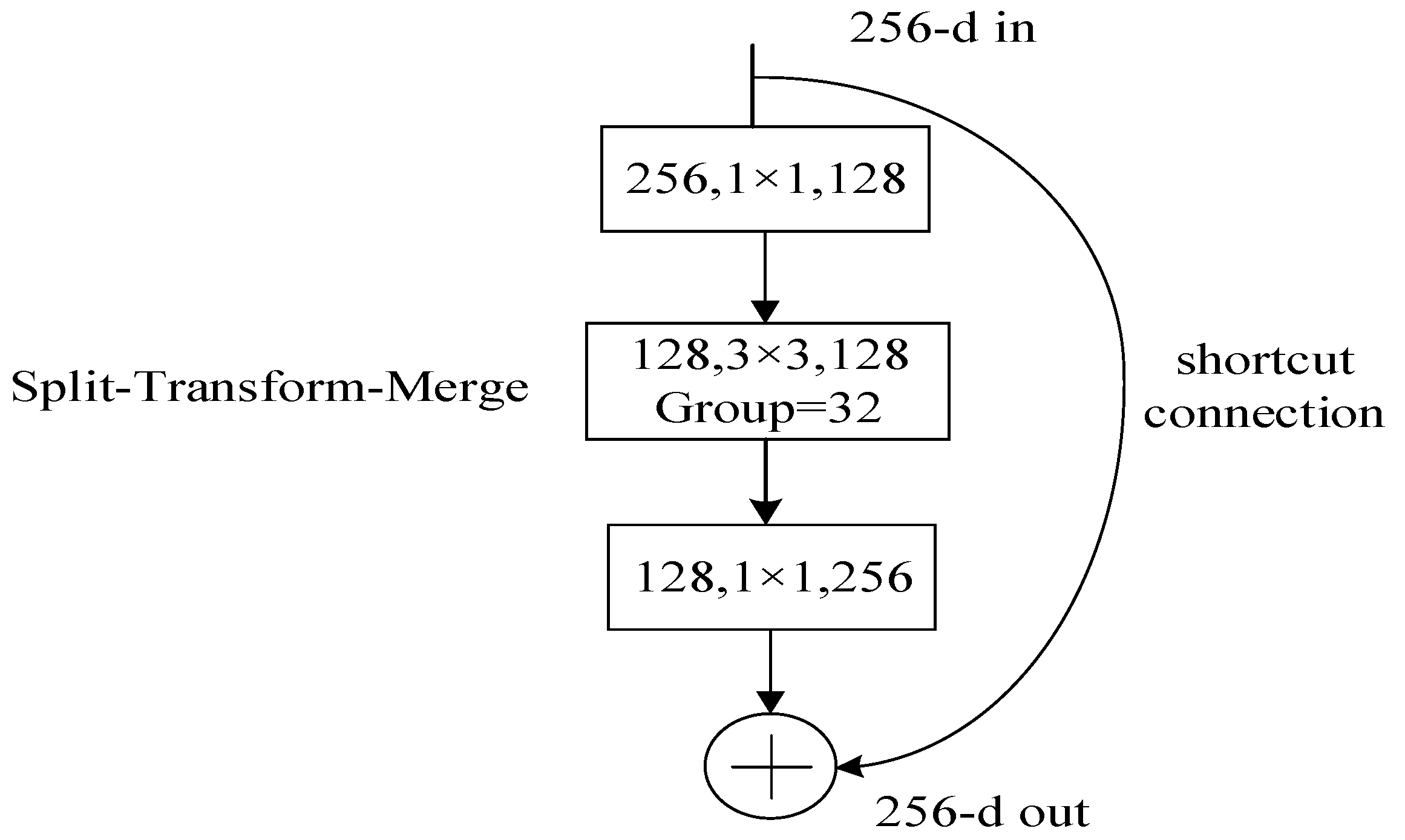
2.2.1. ResNeXt Networking Structure

The ResNeXt structure is constructed using the shortcut connection of the residual network and the split–transform–merge model of the Inception network, based on the repeatedly building of blocks. As shown in Figure 5, the input channels are dimensionally reduced by 1 × 1 filters and separated into different groups with the same structure for group convolution. The calculation outcomes of various groups are integrated, and cardinality is used to control the number of groups. The accuracy of the model can be improved by increasing the number of groups, widening the broadband, and enhancing the network expression. Meanwhile, simplifying the model structure can result in fewer parameters needing to be adjusted and higher scalability [17].

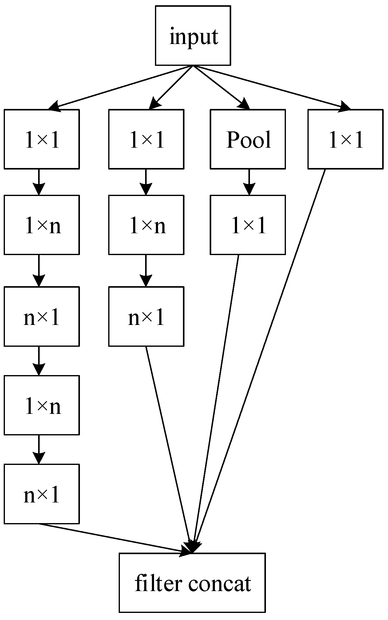
2.2.2. Network Structure of Inception v3

By using the split–transform–merge model, Inception v3 allocates the input to four sub-branches and uses convolutions of various sizes or pools to extract the features from various sizes. Using the concept of factorization into small convolutions, a two-dimension convolution (n × n) can be disassembled into two single-dimension convolutions (1 × n and n × 1). For instance, the features of a 28 × 28 image can be extracted by a 1 × 7 convolution and a 7 × 1 convolution or by a 7 × 7 convolution directly. The features captured by both methods should be the same. As shown in Figure 6, all the outcomes will be integrated using filter concatenation. By disassembling the convolutions of various sub-branches as well as the asymmetric convolutions, the depth of the network can be increased and features with more dimensions can be processed, resulting in more detailed information [18].

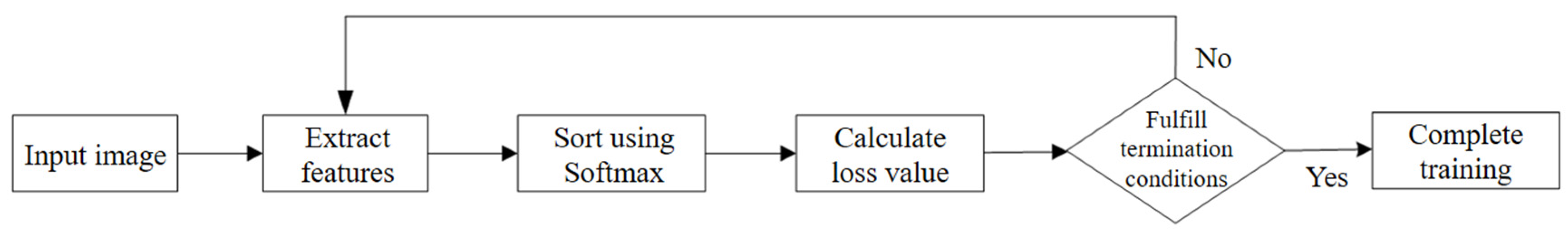
2.2.3. Model Training

As shown in Figure 7, both of the sub-types used for model training followed five steps:
  • input the image;
  • extract the features of the images through the networks and produce a feature map;
  • use SoftMax classification software to transfer the features of the images into probability vectors for k dimension, use elements to express the probability of each class with a range of 0–1 and a sum of 1, and then calculate the probability of the image being in a certain class Equation (2);
  • use Equation (3) to calculate the softmax loss value and then illustrate the prediction errors in the image classification (the deviation degree of the prediction value from the actual value), which should decrease with the training progression;
  • trigger the termination condition (when the largest number of iterations have been reached) to complete the model training.
P j ( x ) = e x T w j k = 1 K e x T w k
where x is the feature value of the image; wj is the weighted value of class j; K is the number of classes; xTwj is the feature value of j reflected in the image; and Pj(x) is the probability of image x being predicted as class j.
S o f t m a x   L o s s = j = 1 K y j l o g ( P j ( x ) )
where yj is the real classification label of the image and is 1 if the real classification label is j, or else 0; Pj(x) is the probability of image x being predicted as class j; and K is the number of classes.

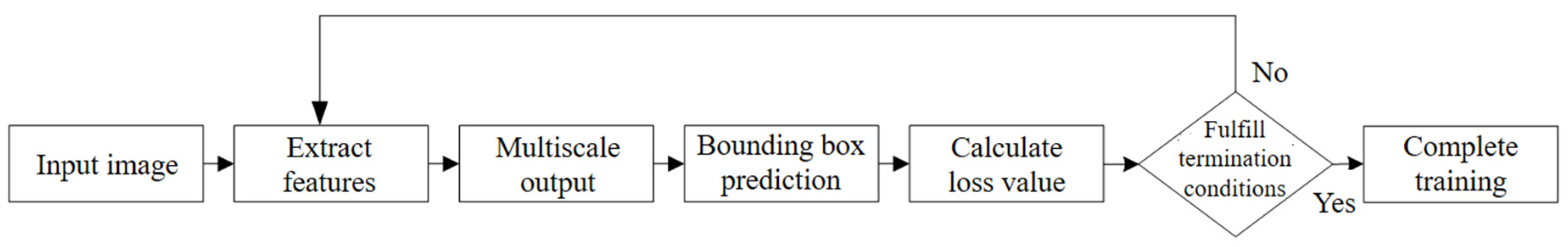
2.3. Training of the YOLO v3 Object Detection Model

The YOLO v3 object detection model, its network structure, model training, and bounding box prediction are described in the following section.

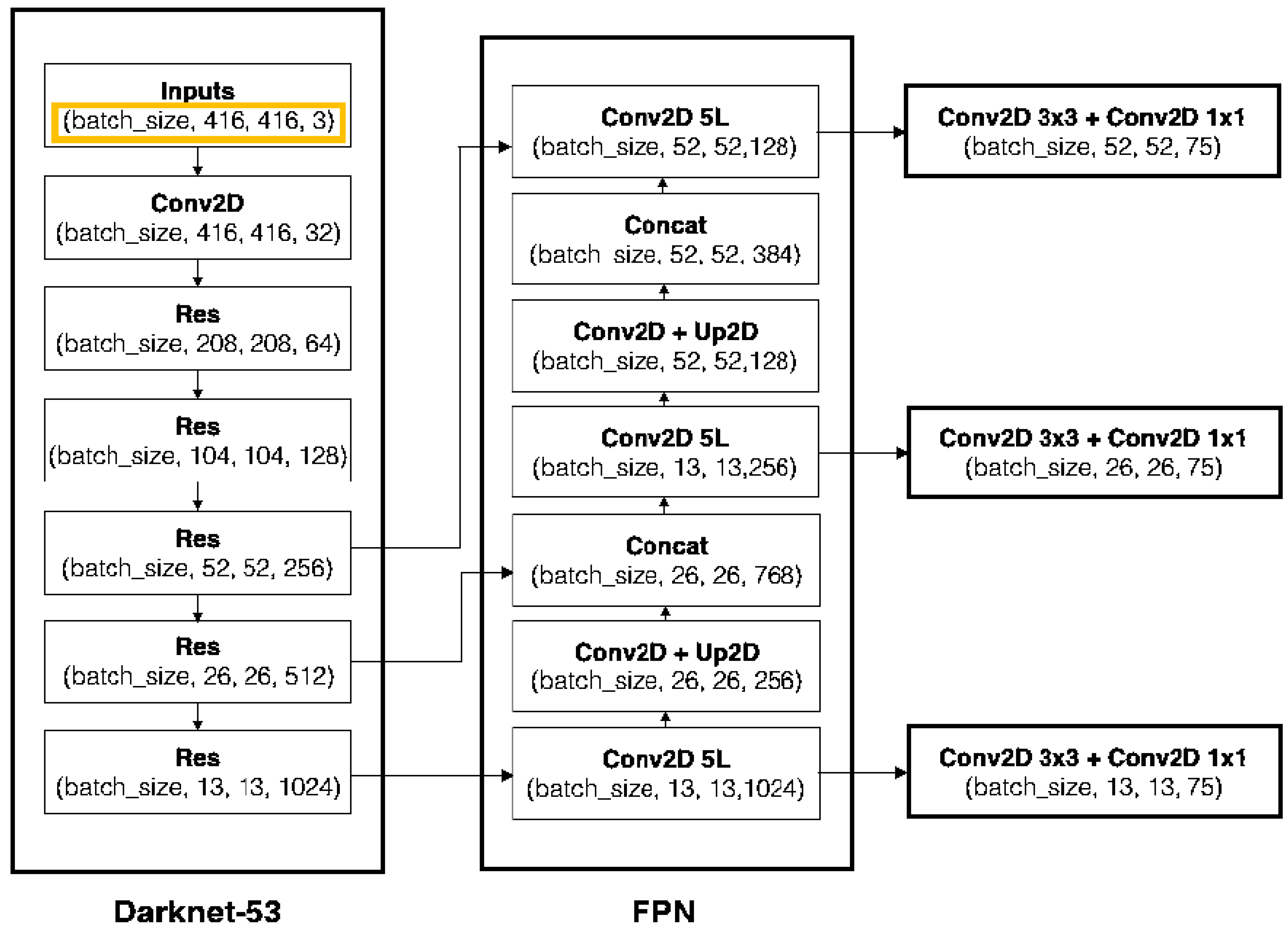
2.3.1. Network Structure

As shown in Figure 8, the YOLO v3 network structure used a residual network to combine high-level defect information and low-level defect information and solve the issue of vanishing gradients. The residual network contained 53 convolutional layers and was called Darknet-53. This model also used feature pyramid networks to improve the ability to predict micro defects. The four figures in the box (batch_size, 416, 416, 3) are respectively the number of image samples captured (batch_size), the size of the images (416 × 416 pixels), and the number of channels (RGB color model) in each batch [19].

2.3.2. Model Training

Figure 9 shows the model training of YOLO v3 in the following seven steps. First, input the image and training parameters such as the frequency of training and the size of the anchor frame. There is a total of 1000 images including standard products and defects for training, testing, and validation. The training set, the validation set, and testing set account for 72%, 18%, and 10%, respectively. Thus, there are 720 images for training, 180 images for validation, and 100 images for testing. Second, extract the features of an image via the residual network. Third, integrate the feature maps via feature pyramid networks, and output the feature maps in three grids sized 13 × 13, 26 × 26, and 52 × 52, respectively, to examine the defects in large to small areas. Fourth, if the center of a defect feature is located in a grid, the model will detect defects within that grid. The detection process is as follows: put the coordinates of the center point of the grid as the center to form three bounding boxes and let the model decide the five parameters of each bounding box (center point coordinates (x, y), width (w), height (h), and confidence). The model then predicts the probability of each classification within each bounding box and chooses the bounding boxes based on the object score for the confidence as well as the non-maximum suppression. Fifth, use Equation (4) to calculate the loss value and continue to update it with the progressing of the training. Finally, trigger the termination condition (when the largest number of iterations have been reached) to complete the model training.
l o s s = λ c o o r d i = 0 S 2 j = 0 B I i j o b j [ ( t ^ x t x ) 2 + ( t ^ y t y ) 2 + ( t ^ w t w ) 2 + ( t ^ h t h ) 2 ] + i = 0 S 2 j = 0 B I i j o b j [ c i log ( c ^ i ) + ( 1 c i ) log ( 1 c ^ i ) ] + λ n o o b j i = 0 S 2 j = 0 B I i j n o o b j [ c i log ( c ^ i ) + ( 1 c i ) log ( 1 c ^ i ) ] + i = 0 S 2 I i o b j c c l a s s e s [ p i ( c ) log ( p ^ i ( c ) ) + ( 1 p i ( c ) ) log ( 1 p ^ i ( c ) ) ]
where λcoord is the weighted loss when the bounding box contains defects (λcoord = 5); and λnoobj is the weighted loss when the bounding box does not contain defects (λnoobj = 0.5). Iiobj means whether the center of the defect falls into the grid. If yes, it is 1, and if no, it is 0. Iijobj means whether the No. j bounding box in grid i is accountable for this default. If yes, it is 1, and if no, it is 0. Iijnoobj means whether the No. j bounding box in grid i is not accountable for this defect. If no, it is 1, and if yes, it is 0. S2 means the image is cut into number S × S of grids; B is the predicted number of bounding boxes (YOLO v3 sets three by default); tx and ty are the deviation value from the coordinates of the real feature box to the left corner of the grid; t ^ x   and   t ^ y are the deviation value from the coordinates of the predicted feature box to the left corner of the grid; tw and th reflect the size scaling from the real feature box to the anchor frame; t ^ w   and   t ^ h reflect the size scaling from the predicted bounding box to the anchor frame; ci is the confidence degree of the real feature box in grid i; c ^ i is the confidence degree of the bounding box in grid i; pi(c) is the probability of the real grid i belonging to class c; and p ^ i ( c ) is the probability of the predicted grid i belonging to class c .

2.4. Testing of the YOLO v3

2.4.1. Testing of the Trained Models

First, based on the labeled defect locations from the input images, Equation (5) is used to calculate the percentage of intersection over union (IoU), in other words, the percentage of overlapping between bounding box A and ground truth B. The larger the value, the more accurate the predictions on the locations of the defects. Then, Equation (6) is used to calculate the confidence degree, which reflects whether the bounding boxes contain features and whether the locations of the features are accurate. Equation (7) is used to calculate the object score of a certain type of confidence, which predicts the probability of the predicted bounding box belonging to the feature classification, which is the accuracy. In the end, the bounding boxes are chosen based on the object score of confidence as well as the non-maximum suppression.
I o U ( A , B ) = A B A B
Confidence = Pr ( O b j e c t ) × I o U
where, if the bounding box contains features, Pr(Object) is 1; otherwise, Pr(Object) is 0.
Pr ( C l a s s i | O b j e c t ) × C o n f i d e n c e = Pr ( C l a s s i ) × I o U
where Pr(Classi|Object) is the probability of the predicted grid features belonging to classification i.

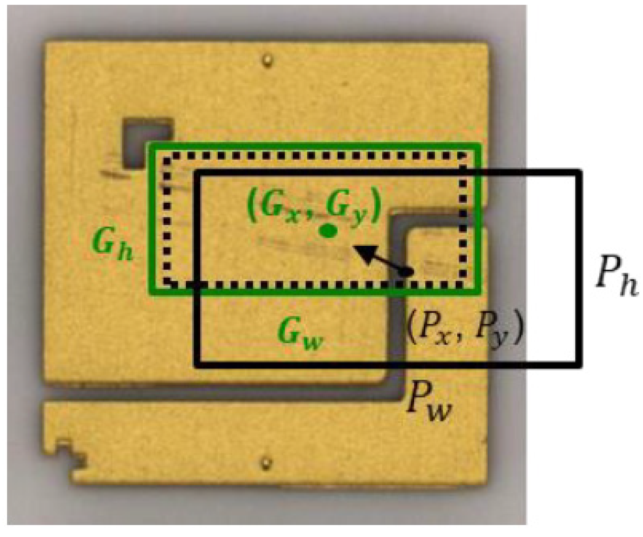
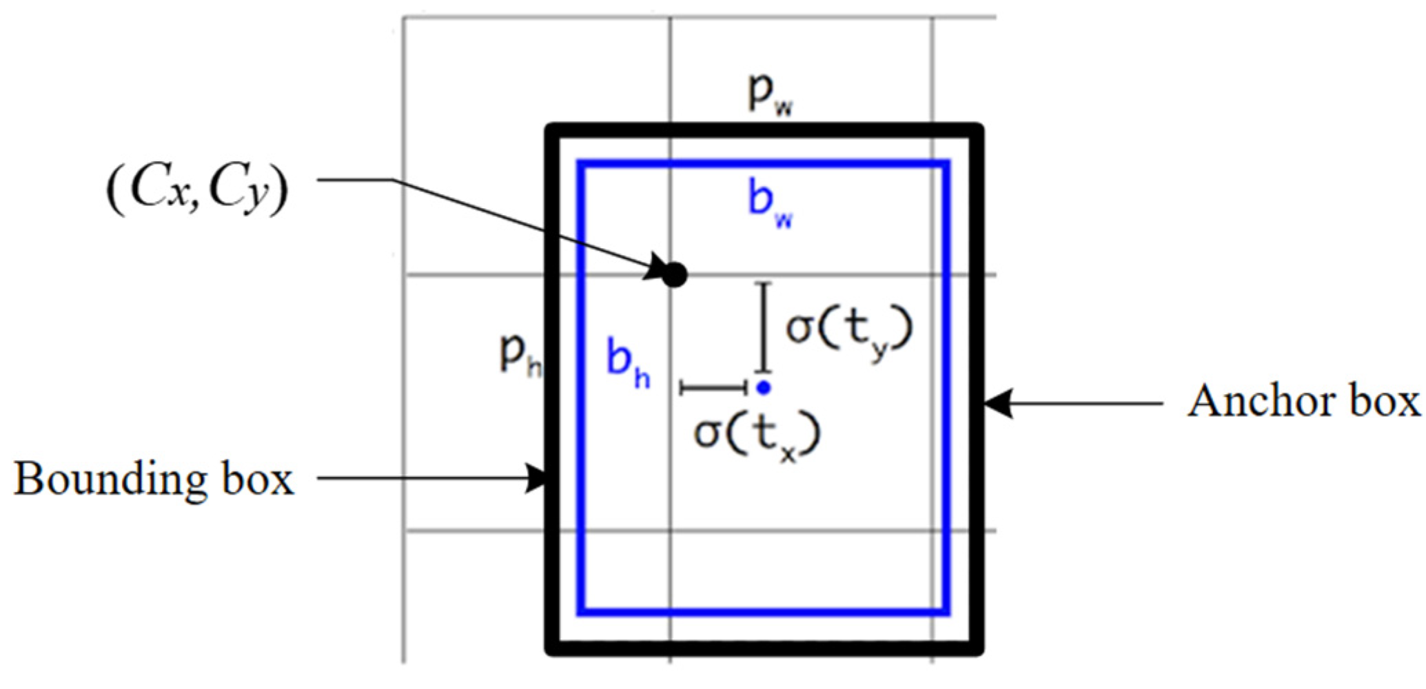
2.4.2. Bounding Box Prediction

The anchor box calculated from Equation (8) of the K-means cluster was used by YOLO v3 to predict the bounding boxes.
d ( b o x , c e n t r o i d ) = 1 I o U ( b o x , c e n t r o i d )
where box is the labeled bounding box; centroid is the initial anchor box; and d ( b o x , c e n t r o i d ) is the percentage of the nonintersection area of the labeled bounding box and initial anchor box.
The learning purposes of YOLO v3 were the deviation value from the grid coordinates to the coordinates of the ground truth box (tx, ty) and the size scaling for the width and height of the pre-set anchor box to the ground truth box (tw, th) as well as the confidence. The learning process is shown in Figure 10, with the black box representing the pre-set anchor box and the green box representing the ground truth box. The moving of coordinates was realized based on Equations (9) and (10), i.e., put the black box with solid lines to the position of the black box with dotted lines, and then based on Equations (11) and (12) (scaling the black box to the size of the green box), where (Gx, Gy), Gw, and Gh are the center point coordinates and the width and height of the ground truth box, respectively, and (cx, cy) are the coordinates of the left corner of the grid.
t x = G x c x
t y = G x c y
t w = log ( G w P w )
t h = log ( G h P h )
Then, substitute t ^ x ,   t ^ y ,   t ^ w ,   and   t ^ h into Equations (13)–(16), respectively, to predict the information of the bounding boxes, where (bx, by), bw, and bh are the center point coordinates and the width and height of the predicted bounding box respectively; σ is a sigmoid function meant to control the deviation value within [0, 1] and prevent over-deviation; (cx, cy) are the coordinates of the left corner of the grid; and Pw and Ph are the width and length of the pre-set anchor box, respectively. Figure 11 illustrates the predicted bounding box [20].
b x = σ ( t ^ x ) + c x
b y = σ ( t ^ y ) + c y
b w = p w e t ^ w
b h = p h e t ^ h

3. Results

3.1. Model Comparison

This paper aimed to discuss the merits and shortcomings of three integrated models: ResNeXt+YOLO v3, Inception v3+YOLO v3, and YOLO v3, and then use testing images to calculate their accuracy and false alarm rates and compare their applications in applicable situations.

3.2. Accuracy Rate and False Alarm Rate

As shown in Table 1 as well as Equations (17) and (18), this research used the accuracy rate and false alarm rate based on the confusion matrix as the performance index of the models, compared the accuracy of different model outcomes on the testing images, and reviewed the improvement effect over AOI. A total of 396 testing images were used for this research, including 98 pictures of contamination defects, 98 pictures of scratch defects, and 200 pictures of standard products. The testing results are shown in Table 2.
A c c u r a c y = T P + T N T P + F P + F N + T N
F a l s e   A l e r m   R a t e = F P T P + F P

4. Discussion

The results showed that the accuracy rates of ResNeXt+YOLO v3, Inception v3+YOLO v3, and YOLO v3 were 99.2%, 98.4%, and 96.2%, respectively, while the false alarm rates were 0%, 0.5%, and 5.8%, respectively. The times used for making predictions were 12 s, 14 s, and 21 s, respectively. The results indicated that ResNeXt+YOLO v3 performed the best and used the shortest time. This was possibly due to the YOLO v3 model learning the locations and categories of images for acquiring more information about defects and being more sensitive to defects in the images, making it easier for it to send false alarms and leading to a lower accuracy rate and higher false alarm rate. The ResNeXt+YOLO v3 model detected the standard images first, thereby decreasing the number of images needing to go through YOLO v3′s image detection and causing the false alarm rate of YOLO v3 to be reduced. In addition, both the ResNeXt model and the YOLO v3 model could capture more features by increasing the broadband, so a higher accuracy rate could be reached. Compared to Inception v3, ResNeXt had more flexibility in the mechanism of increasing the broadband, so it could better learn the images of defects. Therefore, the testing results showed that the ResNeXt+YOLO v3 model had a higher accuracy rate.

4.1. Application Effects and Applicable Scenarios

This study compared the application effects and applicable scenarios of the three integrated models, as shown in Table 3 and in the following section.
Label classification method: The ResNeXt and Inception v3 models could name the folders and store standard/defect images, respectively; YOLO v3 used the LabelImg-master software to label the classification and location of defects.
Building method: All three models conducted model training and testing via a Jupyter notebook. The structures of the integrated classification model and defect detection model required the training of two models respectively, thus the building time was longer and the process was more complicated.
Prediction process: The integrated classification model was faster than the defect detection model. When the two-stage integrated model examined the images, it first classified the standard images and defect images, but only the defect images needed to go through the defect detection of YOLO v3. Therefore, the two-stage integrated model needed a shorter time to make the predictions.
Applicable scenarios: The three integrated models were suitable for examining different images. The sample images used by this research had random locations and multiple forms. The experiment results showed that the YOLO v3 defect detection model often overlooked defects along the edges of the images and often misjudged the images lying between standard and defect. The Inception v3 classification model also had escapes of scratches with a smaller size and multiple forms, but the ResNeXt classification model could detect the standard and defect images more accurately. Thus, the ResNeXt+YOLO v3 integrated model was more suitable for images with defects showing in the center, while the Inception v3+YOLO v3 integrated model was more suitable for images with defects showing in larger sizes, at consistent locations, and in the center. The YOLO v3 defect detection model was more suitable for images with defects showing in the center and images that clearly distinguished immaculacy from defects.

4.2. Effect Analysis

In this research, the AOI technique is used for quality control in the surface-mount technology production to detect the defects in semi-finished/finished products and is widely used for the defect detection of printed circuit boards (PCB) in electronic industries where surface mount technology (SMT) is applied. In this order, we considered a strict threshold value for AOI to prevent ‘escapes’, but this can lead to serious unwanted noise. Therefore, they tend to set up a Noise-Removal procedure after AOI, which increases the computational cost. By applying deep learning to circuit images of the ceramic substrates in AOI, this study aimed to construct an automatic defect detection system that could also identify the categories as well as the locations of defects. Therefore, we proposed and evaluated three models with integrated structures: ResNeXt+YOLO v3, Inception v3+YOLO v3, and YOLO v3. The outcomes indicated that the defect detection system built on ResNeXt+YOLO v3 could most effectively detect standard images that had been misidentified as defects by AOI, categorize genuine defects, and find their location. The testing results showed that the ResNeXt+YOLO v3 integrated model was the best among all three. When it was introduced to the subject company of this study to replace the manual re-examination after AOI, 10 people were needed for manual re-examination before the introduction, and the accuracy rate and false alarm rate of AOI were 85% and 75%, respectively, whereas only one person was needed after the implementation as the person can operate this flaw detection system to conduct an automatic re-examination, and the accuracy rate and false alarm rate can reach 100% and 0%, respectively.

5. Conclusions

With optical examinations widely used in both the high-tech industries and in traditional industries, the demand for higher productivity and quality has continuously increased. Based on the images of ceramic substrates produced by AOI, this research built a defect detection system. By applying deep learning to the defect detection model training through an iterative process, the model was proven to be effective and capable of setting the judging standards. The research proposed and evaluated three models with integrated structures: ResNeXt+YOLO v3, Inception v3+YOLO v3, and YOLO v3. The results indicated that the defect detection system built based on ResNeXt+YOLO v3 could most effectively identify standard images that would be misjudged as defects by AOI and also classify and locate real defects. The system could not only work quickly, but also reach an accuracy rate of 99.2%. At the same time, it could also satisfy the needs of improving the effectiveness and accuracy of AOI, so as to reduce the human resources required by manual re-examination.

Author Contributions

C.-Y.H. drafted the main manuscript and planned the experiments. Y.-L.L. conduct the programming and analysis. I.-C.L. helped in the preparation of the manuscript. All authors have read and agreed to the published version of the manuscript.

Funding

This research received no external funding.

Conflicts of Interest

The authors declare no conflict of interest.

References

  1. Hao, R.; Lu, B.; Cheng, Y.; Li, X.; Huang, B. A steel surface defect inspection approach towards smart industrial monitoring. J. Intell. Manuf. 2020, 32, 1833–1843. [Google Scholar] [CrossRef]
  2. Çelik, A.; Küçükmanisa, A.; Sümer, A.; Çelebi, A.; Urhan, O. A real-time defective pixel detection system for LCDs using deep learning-based object detectors. J. Intell. Manuf. 2020, 31, 1–10. [Google Scholar] [CrossRef]
  3. Tout, K.; Meguenani, A.; Urban, J.; Cudel, C. Automated vision system for magnetic particle inspection of crankshafts using convolutional neural networks. Int. J. Adv. Manuf. Technol. 2021, 112, 3307–3326. [Google Scholar] [CrossRef]
  4. Adibhatla, V.; Chih, H.; Hsu, C.; Cheng, J.; Abbod, M.; Shieh, J. Defect detection in printed circuit boards using you-only-look-once convolutional neural networks. Electronics 2020, 9, 1547. [Google Scholar] [CrossRef]
  5. Li, Y.; Kuo, P.; Guo, J. Automatic Industry PCB Board DIP Process Defect Detection System Based on Deep Ensemble Self-Adaption Method. IEEE Trans. Compon. Packag. Manuf. Technol. 2021, 11, 312–323. [Google Scholar] [CrossRef]
  6. Fupei, W.; Xianmin, Z. Feature-Extraction-Based Inspection Algorithm for IC Solder Joints. IEEE Trans. Compon. Packag. Manuf. Technol. 2011, 1, 689–694. [Google Scholar] [CrossRef]
  7. Ye, Q.; Cai, N.; Li, J.; Li, F.; Wang, H.; Chen, X. IC Solder Joint Inspection Based on an Adaptive-Template Method. IEEE Trans. Compon. Packag. Manuf. Technol. 2018, 8, 1121–1127. [Google Scholar] [CrossRef]
  8. Tsai, D.M.; Huang, C.K. Defect Detection in Electronic Surfaces Using Template-Based Fourier Image Reconstruction. IEEE Trans. Compon. Packag. Manuf. Technol. 2019, 9, 163–172. [Google Scholar] [CrossRef]
  9. Cai, N.; Cen, G.; Wu, J.; Li, F.; Wang, H.; Chen, X. SMT solder joint inspection via a novel cascaded convolutional neural network. IEEE Trans. Compon. Packag. Manuf. Technol. 2018, 8, 670–677. [Google Scholar] [CrossRef]
  10. Ray, S.; Mukherjee, J. A hybrid approach for detection and classification of the defects on printed circuit board. Int. J. Comput. Appl. 2015, 121, 42–48. [Google Scholar] [CrossRef]
  11. Sanguannam, A.; Srinonchat, J. Analysis ball grid array defects by using new image technique. In Proceedings of the 2008 9th International Conference on Signal Processing, Beijing, China, 26–29 October 2008; IEEE: Piscatway, NJ, USA, 2008; pp. 785–788. [Google Scholar]
  12. Abdelhameed, M.; Awad, M.; Abd El-Aziz, H. A robust methodology for solder joints extraction. In Proceedings of the 2013 8th International Conference on Computer Engineering & Systems (ICCES), Cairo, Egypt, 26–27 November 2013; IEEE: Piscatway, NJ, USA, 2013; pp. 268–273. [Google Scholar]
  13. Wu, W.; Chen, C. A system for automated BGA inspection. In Proceedings of the IEEE Conference on Cybernetics and Intelligent Systems, Singapore, 1–3 December 2004; IEEE: Piscatway, NJ, USA, 2004; Volume 2, pp. 786–790. [Google Scholar]
  14. Gao, H.; Jin, W.; Yang, X.; Kaynak, O. A line-based-clustering approach for ball grid array component inspection in surface-mount technology. IEEE Trans. Ind. Electron. 2017, 64, 3030–3038. [Google Scholar] [CrossRef]
  15. Liao, J.Y. The demand for smart detection in the PCB industry is fermented. AOI identification is optimized by AI as a trend. Digitimes 2018.
  16. Aswini, E.; Divya, S.; Kardheepan, S.; Manikandan, T. Mathematical morphology and bottom-hat filtering approach for crack detection on relay surfaces. In Proceedings of the International Conference on Smart Structures and Systems—ICSSS’13, Chennai, India, 28–29 March 2013; pp. 108–113. [Google Scholar]
  17. Xie, S.; Girshick, R.; Dollár, P.; Tu, Z.; He, K. Aggregated residual transformations for deep neural networks. In Proceedings of the IEEE Conference on Computer Vision and Pattern Recognition, Honolulu, HI, USA, 21–26 July 2017; pp. 1492–1500. [Google Scholar]
  18. Szegedy, C.; Liu, W.; Jia, Y.; Sermanet, P.; Reed, S.; Anguelov, D.; Erhan, D.; Vanhoucke, V.; Rabinovich, A. Going deeper with convolutions. In Proceedings of the IEEE Conference on Computer Vision and Pattern Recognition, Boston, MA, USA, 7–12 June 2015; pp. 1–9. [Google Scholar]
  19. Redmon, J.; Farhadi, A. Yolov3: An incremental improvement. arXiv 2018, arXiv:1804.02767. [Google Scholar]
  20. Redmon, J.; Farhadi, A. YOLO9000: Better, faster, stronger. In Proceedings of the IEEE Conference on Computer Vision and Pattern Recognition, Honolulu, HI, USA, 2017, 21–26 July; pp. 7263–7271.
Figure 1. Flow chart of this study.
Applsci 12 02269 g001
Figure 2. Ceramic substrate.
Applsci 12 02269 g002
Figure 3. Grayscale histogram of the ceramic substrates.
Applsci 12 02269 g003
Figure 4. Image features of the ceramic substrates.
Applsci 12 02269 g004
Figure 5. ResNeXt block structure.
Applsci 12 02269 g005
Figure 6. Structure map of the Inception v3 model.
Applsci 12 02269 g006
Figure 7. Classification model training flow chart.
Applsci 12 02269 g007
Figure 8. YOLO v3 network structure map.
Applsci 12 02269 g008
Figure 9. The training process of YOLO v3.
Applsci 12 02269 g009
Figure 10. YOLO v3 training process illustration.
Applsci 12 02269 g010
Figure 11. Predicted bounding box illustration.
Applsci 12 02269 g011
Table 1. Confusion matrix.
Prediction Results
Defect Features ExistDefect Features Does Not Exist
Actual PerformanceDefect Features ExistTrue Positive (TP)False Negative (FN)
Defect Features Does Not ExistFalse Positive (FP)True Negative (TN)
Table 2. Confusion matrix of the testing results.
Predictions
ResNeXt+YOLO v3Inception v3+YOLO v3YOLO v3
ContaminationsScratchesImmaculate ContaminationsScratchesImmaculate ContaminationsScratchesImmaculate
ActualContaminations951295129512
Scratches098009620980
Immaculate 002001019984188
Table 3. Differences among the integrated models.
ResNeXt+YOLO v3Inception v3+YOLO v3YOLO v3
Labeling MethodName folders/
labeling Master
Name folders/
labeling Master
labeling Master
Building MethodMore complicated More complicatedEasier
Prediction ProcessTwo-stageTwo-stageOne-stage
Applicable ScenariosDefects located in the center of the image(i) Larger defects with consistent
locations
(ii) Defects located in the center
of the image
(i) Distinct differences between standard and defect images
(ii) Defects located in the center of the image
Publisher’s Note: MDPI stays neutral with regard to jurisdictional claims in published maps and institutional affiliations.

