Article

The Research on the Signal Generation Method and Digital Pre-Processing Based on Time-Interleaved Digital-to-Analog Converter for Analog-to-Digital Converter Testing

1
School of Automation Engineering, University of Electronic Science and Technology of China, Chengdu 611731, China
2
AVIC Chengdu Aircraft Design & Research Institute, Chengdu 610092, China
*
Author to whom correspondence should be addressed.
Appl. Sci. 2022, 12(3), 1704; https://doi.org/10.3390/app12031704
Submission received: 12 January 2022 / Revised: 30 January 2022 / Accepted: 5 February 2022 / Published: 7 February 2022

Abstract

:
In the high-resolution analog circuit, the performance of chips is an important part. The performance of the chips needs to be determined by testing. According to the test requirements, stimulus signal with better quality and performance is necessary. The main research direction is how to generate high-resolution and high-speed analog signal when there is no suitable high-resolution and high-speed digital-to-analog converter (DAC) chip available. In this paper, we take the high-resolution analog-to-digital converter (ADC) chips test as an example; this article uses high-resolution DAC chips and multiplexers to generate high-resolution high-speed signals that can be used for testing high-resolution ADC chips based on the principle of time-alternating sampling. This article explains its method, analyzes its error and proposes a digital pre-processing method to reduce the error. Finally, the actual circuit is designed, and the method is verified on the circuit. The test results prove the effectiveness of this method for generating high-resolution ADC test signals.

1. Introduction

Circuits in electronic devices are mainly composed of two parts: digital circuits and analog circuits. In mixed analog–digital circuits, analog circuits account for a small percentage, but the failure rate of analog circuits is high [1]. Analog circuit test has become the last barrier to ensure the stability and reliability of analog circuits [2]. Analog circuit test is generally divided into two stages, applied stimulus and response analysis, where the applied stimulus signal requires a signal with an accuracy level higher than that of the circuit under test [3]. In analog circuit testing, analog-to-digital converter (ADC) chip testing is a major part of testing.
In large-scale semiconductor chip production [4,5,6], chip testing mainly uses automatic test equipment (ATE). ATE is a high-performance test device controlled by a computer. When testing the ADC chip, it mainly uses the arbitrary waveform generator equipment in the ATE to provide the input signal, then uses the tested ADC to collect the output signal of the arbitrary waveform generator and then calculates and evaluates the collected signal. The computer sends control commands to the digital signal processor. The digital processor generates the waveform required by the test, and the generated waveform is applied to the ADC under test through an optional filter. The data obtained by ADC are then transmitted to the computer for judgment after digital processing to determine whether the tested ADC meets the requirements. The structure diagram of the ADC test scheme is shown in Figure 1.
At present, 16-bit resolution arbitrary waveform generators are mainly used for ATE testing. According to the type, it can be divided into desktop and board type. The representative of the desktop arbitrary waveform generator is mainly the AWG5200 series of Tektronix [7], and the representative of the board type arbitrary waveform generator is mainly the PXIe-5423 series of American Instruments [8]. In addition, there are some arbitrary waveform generators with 24-bit resolution, but their sampling rate is relatively low. For example, the resolution of PXI arbitrary waveform generator of APPLICOS PG24192 model can reach 24 bits, but the sampling rate is only 192 ksps [9]. According to the IEEE 1241 [10] standard, in the ADC test, a waveform with a higher resolution than the ADC under test should be used. Therefore, for 18-bit, 20-bit and other high-precision ADC chips, 24-bit resolution signals are required for testing. For example, to measure an ADC chip with a resolution of 20 bits and a sampling rate of 1 MHz, the signal is required with at least a resolution of 24 bits and a frequency of 500 KHz. However, the signal generator is currently unable to generate such a signal. Therefore, the design and testing of high-resolution and high-speed signal generation methods are currently being studied both at home and abroad. For the required waveform generation method for high-precision ADC testing, the main research directions at home and abroad are divided into two directions: generating high-purity sine wave signals through existing low-resolution DACs and directly designing higher-resolution DAC chips [11,12].

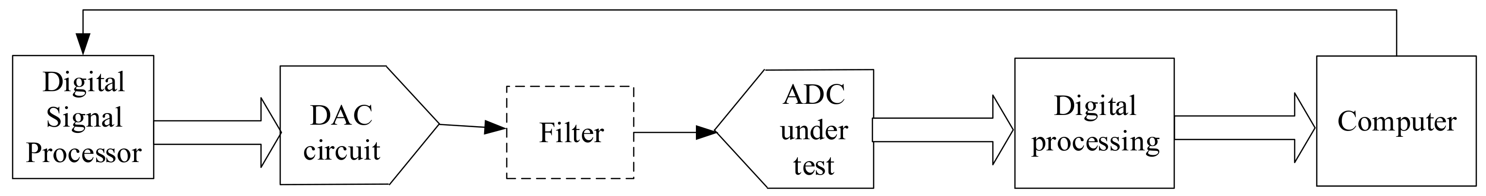
2. Related Works and Problems

In response to the demand for such high-resolution and high-speed signals, research is being conducted at home and abroad. Reference [13] proposes a way to improve the resolution of the system by using two programmable gain amplifiers (PGA) at the back end of the DAC [13]. The PGA is controlled by a digital signal processor (DSP) and can amplify or attenuate the output signal of DAC. In this way, a smaller amount of variation than the minimum signal step output by the DAC itself can be obtained. The structure diagram of the method is shown in Figure 2. The relative resolution of the system is improved by amplifying the output voltage amplitude of the system, but in fact, its absolute resolution, that is, the minimum output voltage step, remains unchanged. When measuring a small range ADC, the problem still exists that the resolution of the signal’s resolution is not high enough. In addition, the system will send digital quantities to DAC and PGA at the same time, but the response is not synchronized. It will affect the quality of the output waveform.
Reference [14] proposes a method of superimposing the output of several DACs together to improve system resolution [14]. Its system structure is shown in Figure 3. It uses four 8-bit DACs to achieve the effect of a 32-bit resolution digital-to-analog (DA) conversion circuit. The principle is to use the difference of the resistance in the addition circuit to achieve different magnifications. This method can improve the resolution of the DA conversion circuit. However, there is a problem in the actual circuit that it is difficult to achieve a strict multiple relationship of the resistance value due to the accuracy of the resistance. In addition, the thermal noise of the resistance [15], the asynchronous transmission delay of the amplifier [16] and the asynchronous output of different DACs will also have a greater impact on the system output, resulting in a reduction in the signal-to-noise ratio (SNR) of the output signal.
Considering the influence of power supply on DAC reference voltage and amplifier [17,18,19], the influence of temperature on resistance noise [20,21,22], without considering the additional processing of power supply, the time alternating circuit we designed needs to use the same type of DACs and the same channel structure and avoid the use of resistance weighted network [23]. Therefore, in view of the above problems, this article proposes a method to generate high-resolution and high-speed signals for ADC testing based on the principle of time-interleaving by using high-resolution DAC.

3. Signal Generation Method and Circuit Design Based on Time-Interleaving

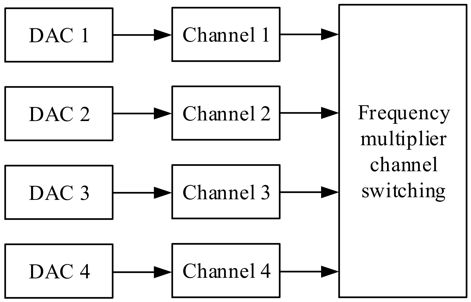
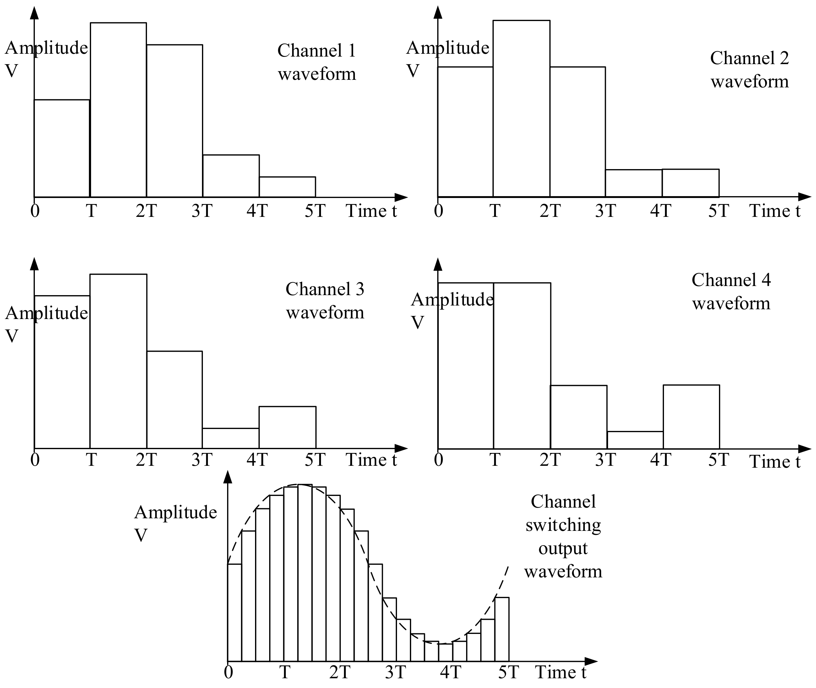
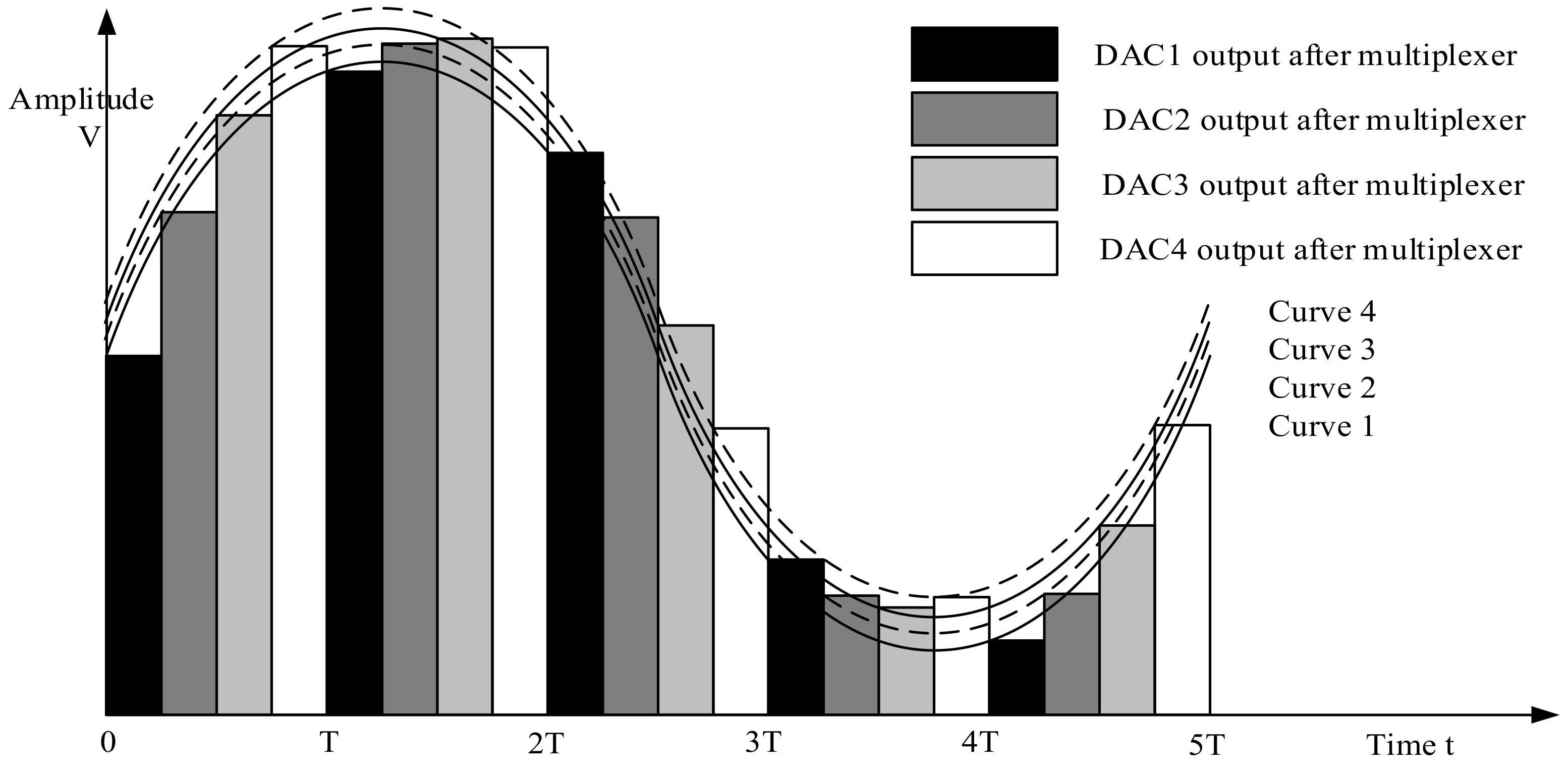
3.1. Signal Generation Method Based on TIDAC
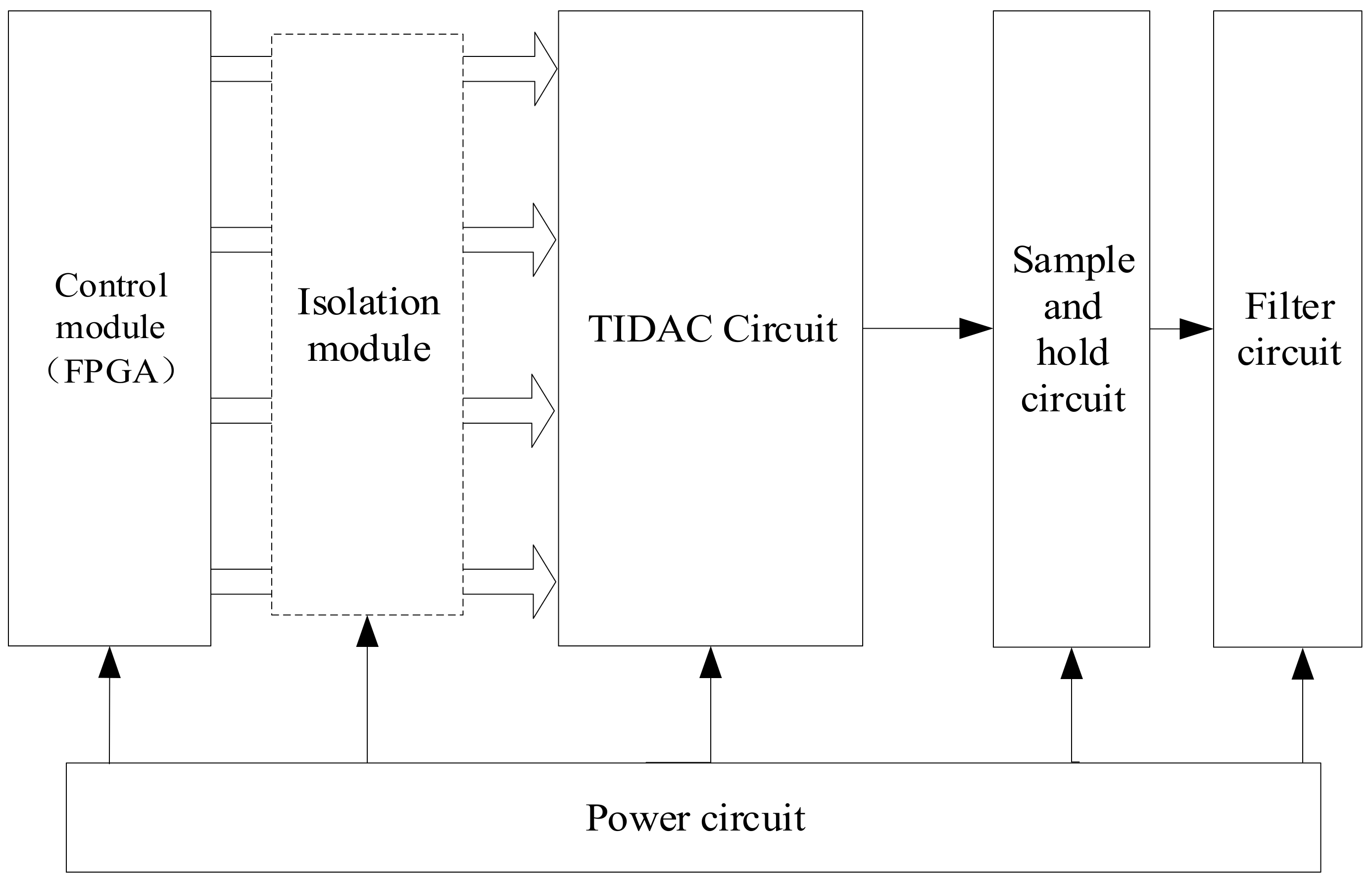
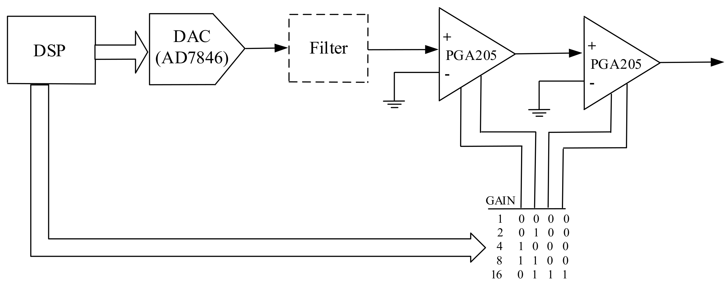
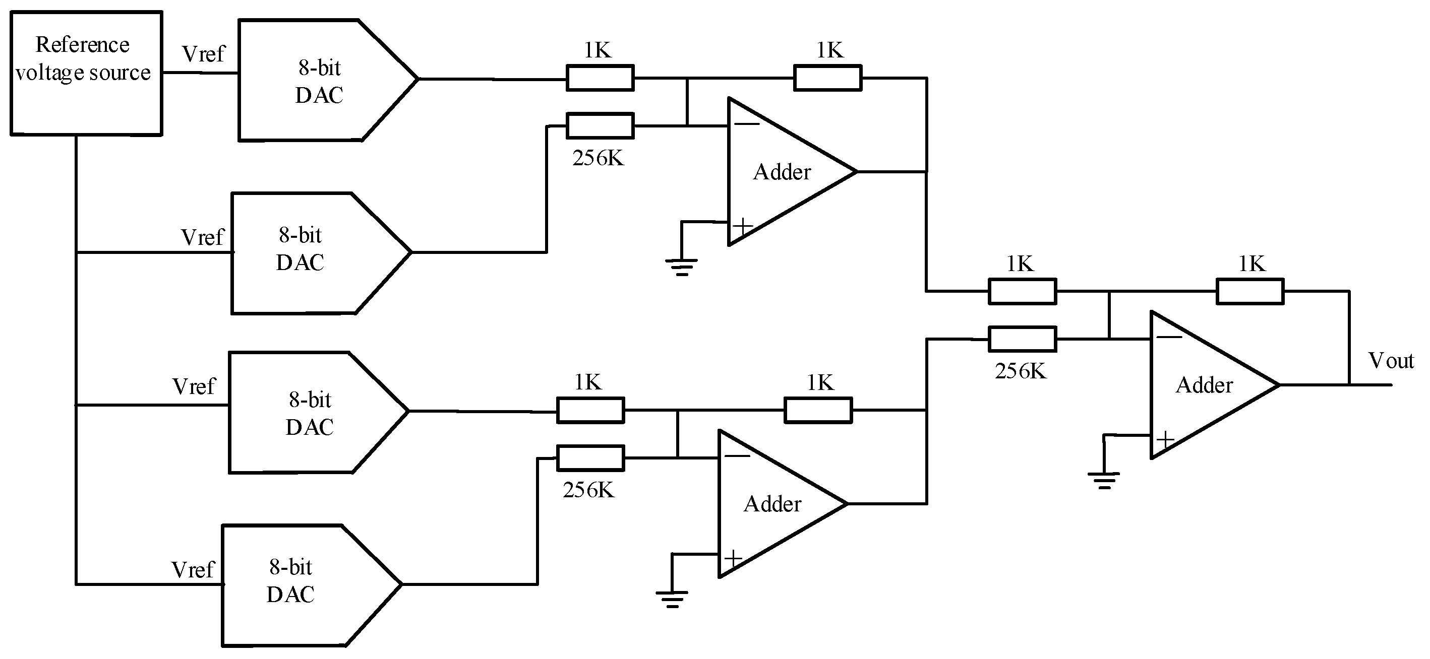
The TIDAC-based method uses multiple high-resolution DACs and selects different DAC output channels for output through a channel switching circuit. Switch between multiple DAC output channels at higher frequencies and realize a high-resolution and high-speed DA conversion circuit with multiple sampling rates on the basis of the original high-precision DAC. The signal generation circuit structure model based on TIDAC is shown in Figure 4.
The 4 channels work at the sampling rate of fs, respectively, and the frequency multiplier channel is switched at a frequency of 4 fs to switch among the 4 output channels in turn, realizing high-speed sampling on the original high-precision DAC. After the channel switching, the analog signal is collected and output by the acquisition and holding module at a frequency of 4 fs to reduce the influence caused by the channel switching. Theoretically, the relationship between the 4 channel outputs in TIDAC and the channel switching output is shown in Figure 5.
In the figure, each channel outputs a level value every sampling period T. When the time belongs to 0~1/4T, the output channel is switched to channel 1, and the level value of channel 1 is output. When the time belongs to 1/4T~1/2T, the output channel is switched to channel 2, and the level of channel 2 is output value. When the time belongs to 1/2T~3/4T, the output channel is switched to channel 3, and the level value of channel 3 is output. When the time belongs to 3/4T~T, the output channel is switched to channel 4, and the level value of channel 4 is output. Then, when the time belongs to T~5/4T, the output channel is switched to channel one again, and the level value of channel one is output, and so on; the multiplexer switches the output evenly among the four channels and is multiplexed. The output waveform after the converter is shown in Figure 3. Comparing these figures, it can be seen that under the same output frequency, the sampling point of the multiplexer output waveform is 4 times the number of sampling points output by a single channel, that is, the sampling rate of the system is relative to the sampling rate of the original DAC. Improved by 4 times.

3.2. Circuit Design

Based on the above analysis, this circuit selects the AK4490 high-resolution DAC chip from AKM Company. The channel switching module selects the multiplexer chip. The output of the multiplexer is sampled and held by the sample-and-hold. Then, a high-order low-pass filter for filtering processing is designed, so that the output waveform of the system changes from a ladder to a smooth waveform. By controlling the channel switching of the multiplexer, the output step number of the entire system becomes 4 times that of the original single DAC output step number, that is, the sampling rate of the original DAC is increased by 4 times. Figure 6 shows the overall design of the TIDAC-based high-resolution and high-speed signal generation circuit.
In the control module, the field programmable gate array (FPGA) provides digital quantities to the 4 DACs of the TIDAC module; the TIDAC circuit mainly includes a DAC circuit, a reference power supply circuit, a channel amplitude control circuit and a channel switching circuit. The reference voltage of each DAC in TIDAC is the same and all work at the maximum sampling frequency. Then, the 4 DACs respectively output the corresponding analog waveforms, then respectively pass the corresponding 4 channel amplitude control circuits to fine-tune the amplitude and then output to the multiplexer for selection output. The analog signal output by the TIDAC circuit enters the sample-and-hold circuit and is sample-and-held output at a certain frequency; the waveform output by the sample-and-hold circuit is a ladder wave, which is filtered by the filter circuit to finally output a smooth waveform. The power supply module is the power supply module of the system, and all the device work is provided by it.

4. Error Analysis and Processing

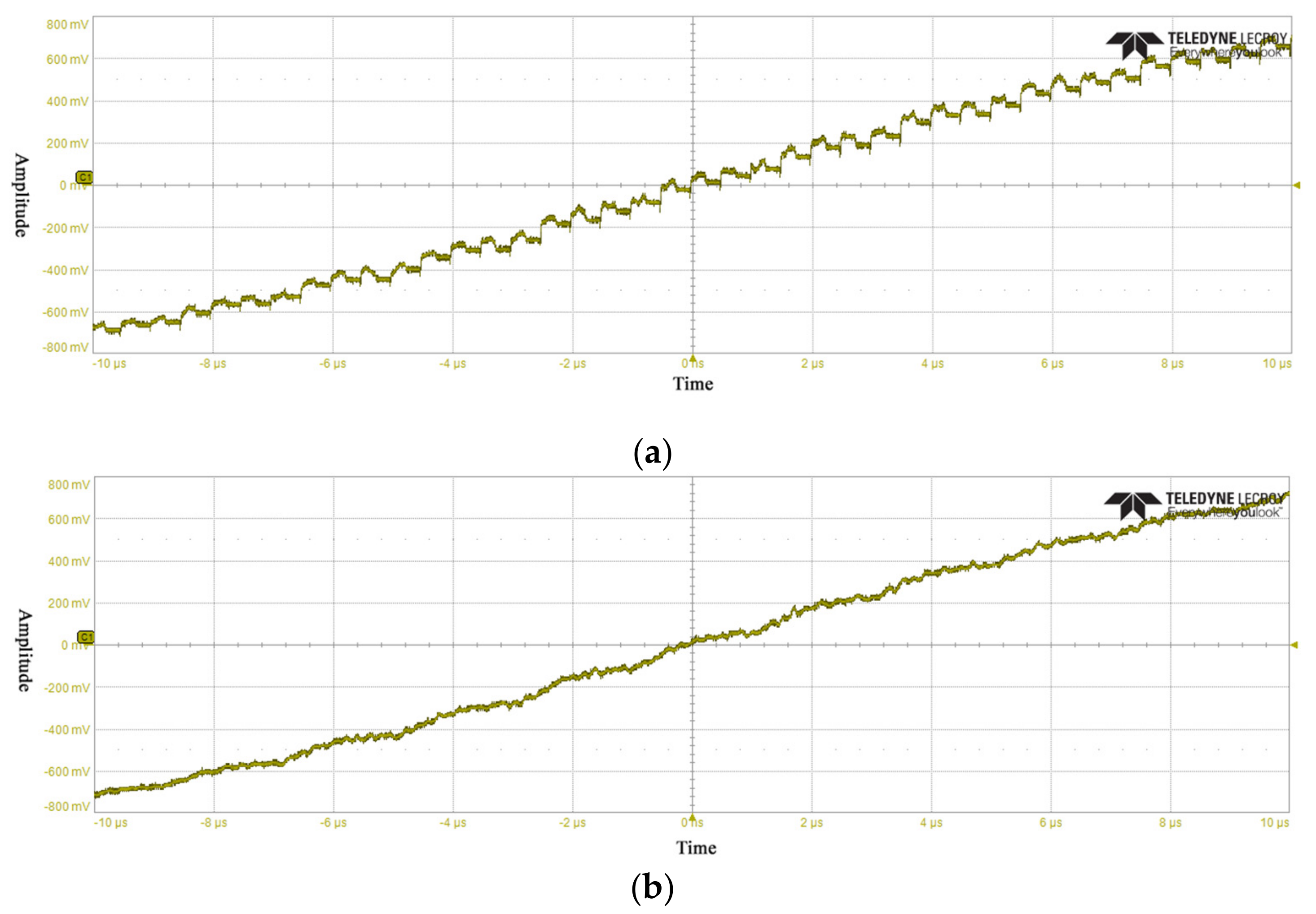
4.1. Amplitude Error Analysis and Digital Pre-Processing

In the case of a single DAC sampling output, the gain offset error of the DAC can be found by querying the data sheet of the DAC, which is a relatively fixed parameter. In general, there is a relationship between the input digital quantity and the output analog quantity of the DAC:
V o u t = D 2 N · V r e f
In the formula, N represents the resolution of the DAC, Vref represents the DAC reference voltage, D represents the input digital quantity and Vout represents the output analog quantity.
In this circuit, there is a relationship between the output analog quantity of the four DAC outputs and the input digital quantity of the DAC after passing through the channel amplitude control circuit and the different channels of the multiplexer:
V o u t 1 = A 1 · D 2 N · V r e f ; V o u t 2 = A 2 · D 2 N · V r e f V o u t 3 = A 3 · D 2 N · V r e f ; V o u t 4 = A 4 · D 2 N · V r e f
In the formula, Vout1, Vout2, Vout3 and Vout4 are, respectively, the output voltage value after the output of DAC1 to DAC4 switched by the multiplexer. A1, A2, A3 and A4 are different. Therefore, it can be found that when the same digital quantity is given to four DACs, the output analog quantity is not the same. In addition, because of the slight difference in the gain of each channel of the multiplexer, the same input analog quantity enters different channels of the multiplexer, and there may be slight differences after the output. Therefore, in order to ensure that when the same digital quantity is input, the same analog quantity can be output after passing through different channels and, finally, after the multiplexer, it is necessary to calibrate and process the gain errors of different channels. When we give the prestored standard sine wave digital quantities to the four DACs, the output of the blocking multiplexer is shown in Figure 7.
We can represent the four curves separately, namely:
x 1 t = A 1 · sin 2 · π · 1 5 · T · t x 2 t = A 2 · sin 2 · π · 1 5 · T · t x 3 t = A 3 · sin 2 · π · 1 5 · T · t x 4 t = A 4 · sin 2 · π · 1 5 · T · t
Assuming that the output waveform of DAC1 is used as the standard sine wave. So, only the waveform data of DAC2, DAC3 and DAC4 need to be modified so that the waveform data of them can meet the value of the waveform data of DAC1. To make the output waveforms of the remaining DACs match the output waveforms of DAC1, the outputs of the remaining DACs can be multiplied by the corresponding coefficients k. For the k, there are the following formulas:
k 2 = x 1 t x 2 t = A 1 A 2 ;   k 3 = x 1 t x 3 t = A 1 A 3 ;   k 4 = x 1 t x 4 t = A 1 A 4
Therefore, after the corresponding coefficient is obtained by measurement, the digital quantity can be multiplied by the corresponding coefficient through the relationship in Formula (1), and then the amplitude error calibration can be realized by giving the corresponding DAC.
Through experimental testing and verification, the output waveform result is shown in Figure 8:
Comparing the two graphs in Figure 8, it is obvious that the output waveform after amplitude calibration is smoother and conforms to the standard sine wave.

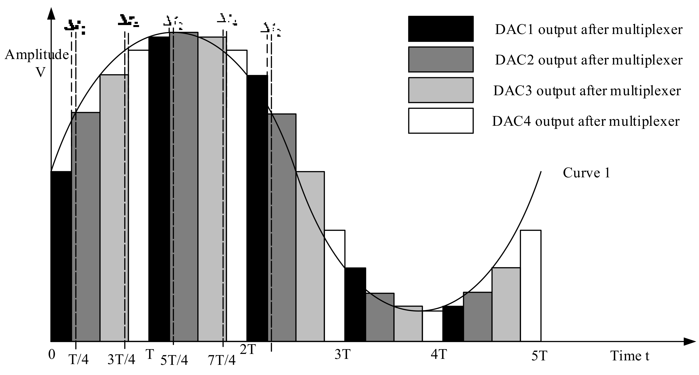
4.2. Time Error Analysis and Digital Pre-Processing

In this circuit design, when the output switching time is completely ideal, the multiplexer output waveform is shown in Figure 5, which can be expressed as:
x t = A · sin 2 · π · 1 5 · T · 0 + b , 0 t < T 4 ; A · sin 2 · π · 1 5 · T · T 4 + b , T 4 t < T 2 ; A · sin 2 · π · 1 5 · T · T 2 + b , T 2 t < 3 · T 4 ; A · sin 2 · π · 1 5 · T · 19 · T 4 + b , 19 · T 4 t < 5 · T ;
Which can be reduced to:
x t = A · sin 2 · π · 1 5 · T · n · T 4 + b = A · sin n · π 10 + b , n · T 4 t < n + 1 · T 4 ; n = 0 , 1 , 2 18 , 19 ;
In the formula, when n is 0, 4, 8, 12, 16, the corresponding output from DAC1 is the output value after channel switching; when n is 1, 5, 9, 13, 17, the corresponding output from DAC2; When n is 2, 6, 10, 14, 18, the corresponding output from DAC3 is the output value after channel switching; when n is 3, 7, 11, 15, 19, the corresponding output value from DAC4 is output after channel switching.
When the switching time of the multiplexer is uneven, the duration of each channel will be uneven, as shown in Figure 9.
In the figure, it can be found that the width of the waveform output by each DAC, that is, the output duration, is not the same. In this case, small burrs with depressions or protrusions will appear on the final output waveform, which will affect the quality of the output waveform. Therefore, the time error needs to be tested and calibrated.
Due to the low frequency of this circuit, the time delay error can be measured with a high-speed digital oscilloscope. The output delay is mainly measured from the output pin of the DAC to the output pin of the multiplexer. So, you can let the DAC output a fixed frequency clock signal, use the two acquisition channels of a dual-channel high-speed oscilloscope to measure the output pin of the DAC and the output pin of the multiplexer at the same time and measure the delay through the measurement function of the oscilloscope.
Assuming that the output delay of DAC1 is taken as the standard, first control the multiplexer to select the output channel of DAC1, then measure the output of DAC1 and the output of the multiplexer at the same time and record the time delay as t1; then, control the multiplexer in turn. The multiplexer selects the output channels of DAC2, DAC3 and DAC4, respectively, and then respectively measures the delay between the output pin of the DAC and the output pin of the multiplexer when the corresponding DAC is strobed, which are respectively marked as t2, t3 and t4, then we can obtain:
Δ t 2 = t 2 t 1 ; Δ t 3 = t 3 t 1 ; Δ t 4 = t 4 t 1 ;
In the formula, Δt2, Δt3 and Δt4 are, respectively, the output time error of DAC2, DAC3 and DAC4 output through the multiplexer and DAC1 output through the multiplexer. Therefore, the time error Δt of different channels can be obtained by measuring the time delay, as shown in Figure 10.
Combined with Figure 10, using the reflection of the time error on the amplitude error, the time error is quantitatively analyzed and researched. It can be seen from the figure that when the time error is Δt, the corresponding value of curve 1 has a difference of Δy from the actual output value. Therefore, it is only necessary to find the corresponding output analog value when the time error is Δt, and then change the corresponding input digital value, so that the output analog value of the corresponding DAC can be outputted as a sine wave after passing through the multiplexer. The value of the waveform.
When DAC2, DAC3 and DAC4 output waveforms and the output time error after multiplexer switching are Δt2, Δt3 and Δt4, respectively, the output waveforms of DAC2, DAC3 and DAC4 after passing through the multiplexer can be expressed as follows.
The DAC2 output:
x 2 t = A · sin 2 · π · 1 5 · T · n · T 4 + Δ t 2 + b = A · sin n · π 10 + 2 · π · Δ t 2 5 · T + b , n · T 4 + Δ t 2 t < n + 1 · T 4 + Δ t 3 ; n = 1 , 5 , 9 , 13 , 17 ;
The DAC3 output:
x 3 t = A · sin 2 · π · 1 5 · T · n · T 4 + Δ t 3 + b = A · sin n · π 10 + 2 · π · Δ t 3 5 · T + b , n · T 4 + Δ t 3 t < n + 1 · T 4 + Δ t 4 ; n = 2 , 6 , 10 , 14 , 18 ;
The DAC4 output:
x 4 t = A · sin 2 · π · 1 5 · T · n · T 4 + Δ t 4 + b = A · sin n · π 10 + 2 · π · Δ t 4 5 · T + b , n · T 4 + Δ t 4 t < n + 1 · T 4 ; n = 3 , 7 , 11 , 15 , 19 ;
Therefore, the digital quantity in DAC2 needs to be updated, and the digital quantity corresponding to the analog waveform value in Formula (8) is given to DAC2, and then output by it, the output waveform can conform to the corresponding output waveform of DAC1. In the same way, the pre-stored waveform data of DAC3 and DAC4 also need to be updated accordingly. According to the previously measured time error Δt3 and Δt4, combined with Formulas (8) and (10), the simulation value is calculated and updated.
After obtaining the analog voltage values required by the new DAC2, DAC3 and DAC4, use Formula (1) to obtain the digital quantity corresponding to each analog value, and then store it in the corresponding storage space to collect and output for the DAC.

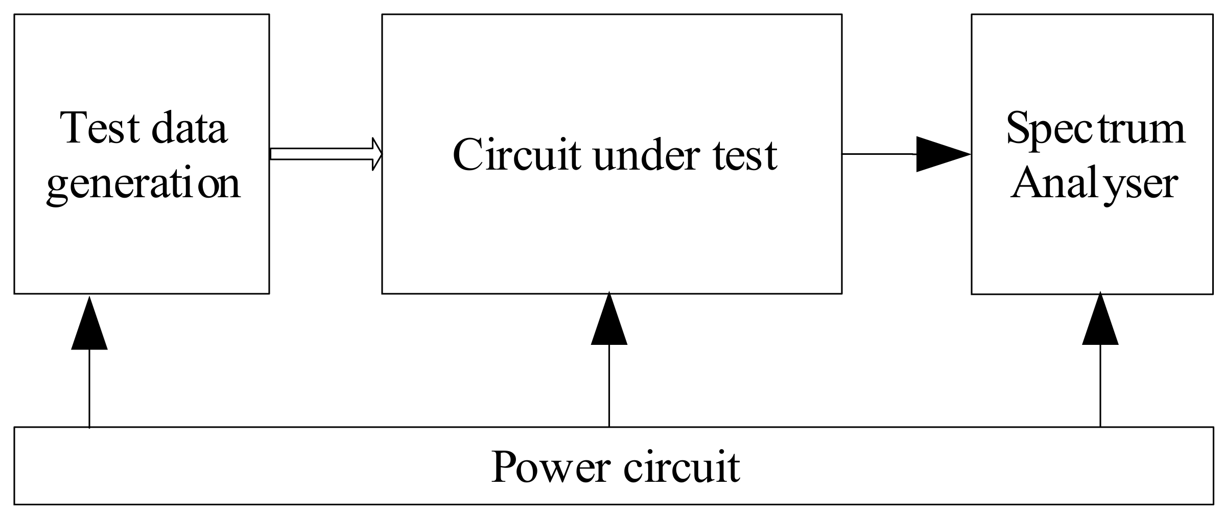
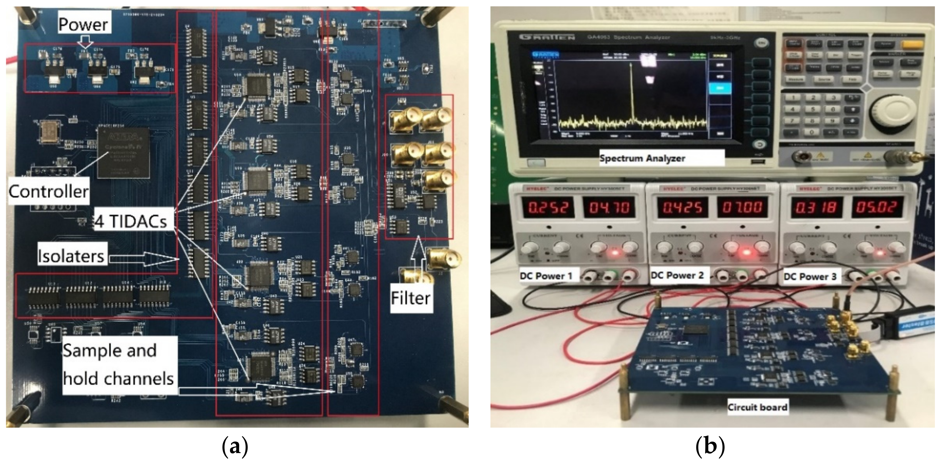
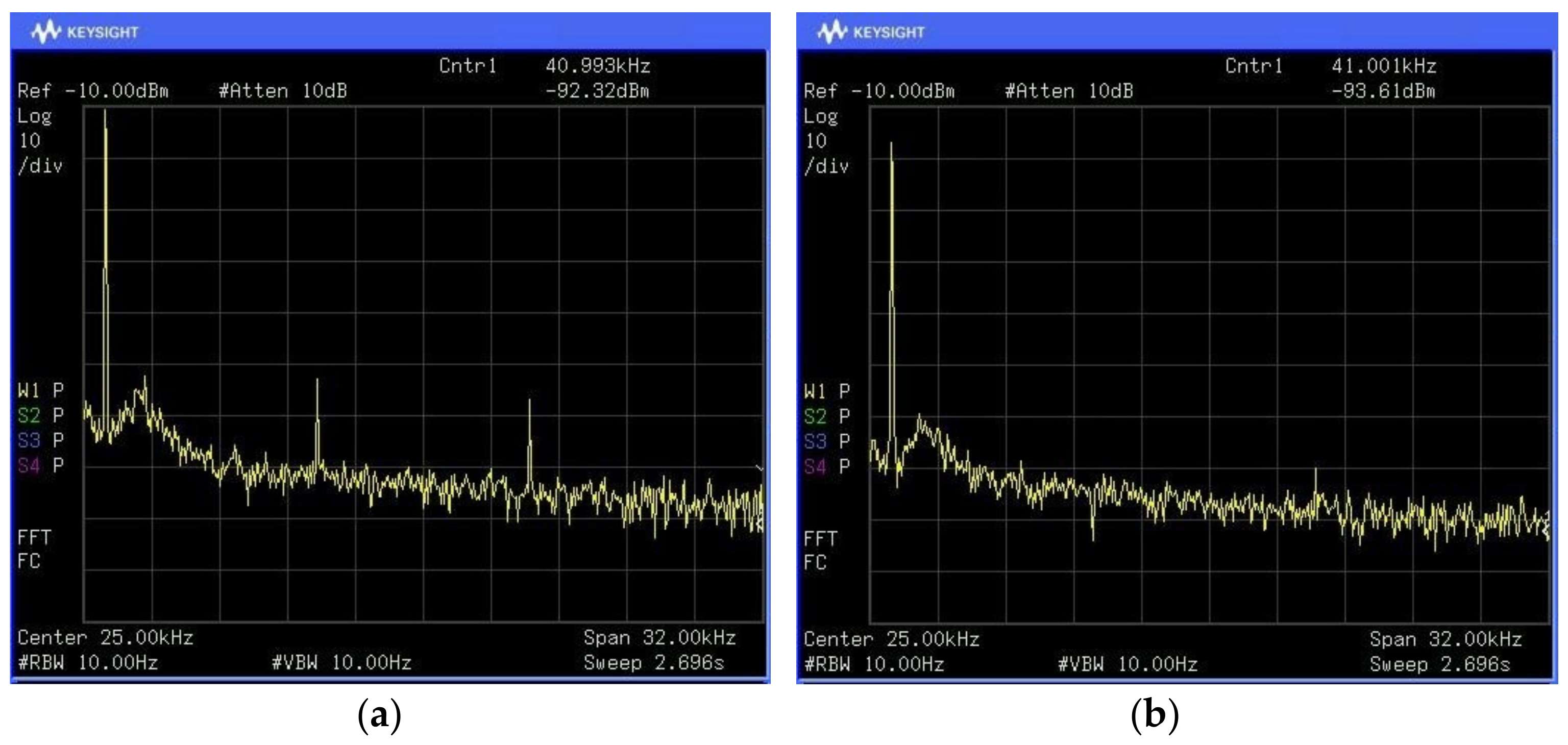
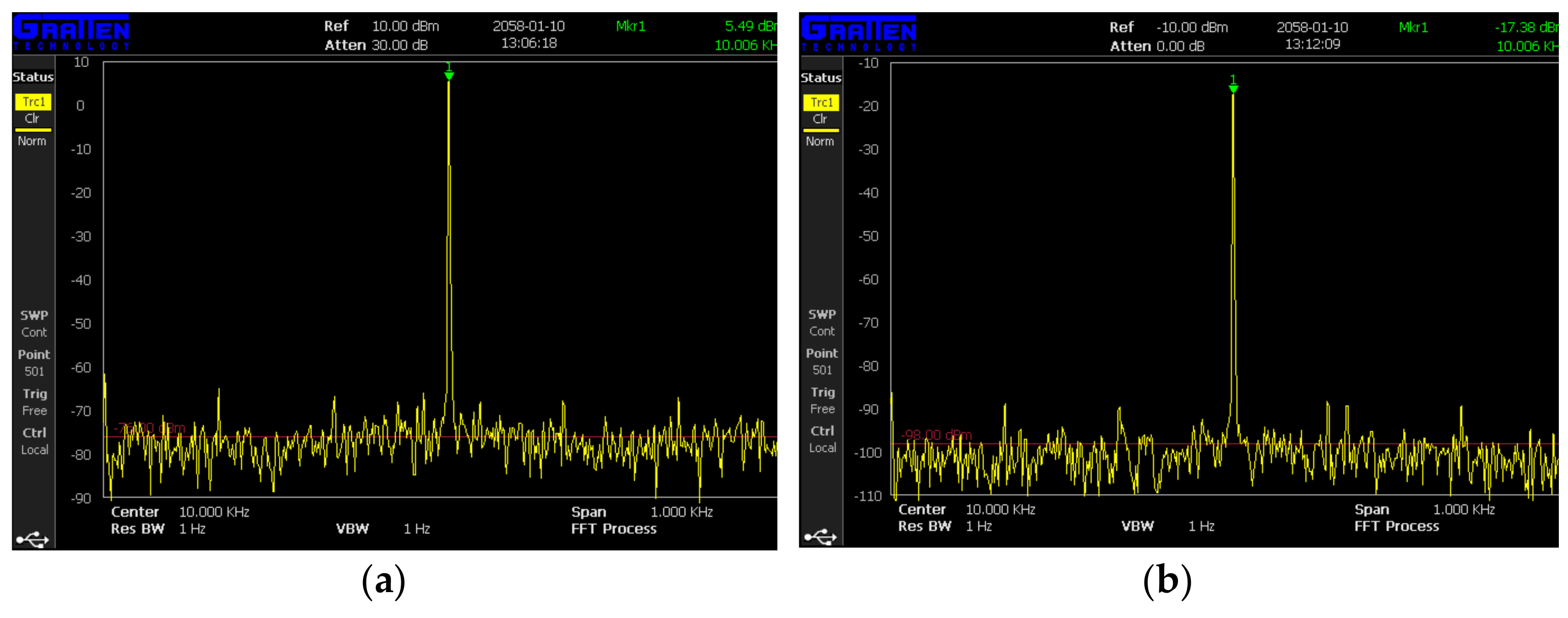
5. Test Results and Analyses

Use a spectrum analyzer to measure the quality of its output signal, that is, the SNR. The test block diagram is shown in Figure 11.
According to this scheme, the specifically designed circuit board and the actual test connection diagram are shown in Figure 12.
When using a spectrometer to test the SNR, due to the limitation of the dynamic range of the spectrometer, it is necessary to observe the power of the output signal and the power of the output noise under different attenuation degrees. Because of the system noise figure in the spectrum analyzer and the distortion performance of the input mixer, the dynamic range of the spectrum analyzer is inconsistent with its measurable range, and appropriate test parameters need to be set according to the specific situation [24]. For the test of this subject, the GA4063 type spectrum analyzer was used. It has a measurable range of +30 dBm to −148 dBm. In addition, the unit of spectrum analyzer is dBm, which is different from the unit of SNR, dB. So, after obtaining the test results, we need to calculate the SNR through Formula (11). The SNR is equal to the power of the signal minus the power of the noise.
S N R d B = 10 log 10 P s i g n a l m W P n o i s e m W = 10 log 10 10 P s i g n a l d B m 10 10 P n o i s e d B m 10 = P s i g n a l d B m P n o i s e d B m
Firstly, we measured the signal before and after the filter. The result is shown in Figure 13.
In Figure 13, the frequency of the tested signal is 10 KHz. The span of the spectrum analyzer is set as 32 KHz, which can include the second, third and fourth harmonics. From Figure 13a, it can be found that the second and third harmonic components are a bit high. However, in Figure 13b, the harmonic components of the signal are reduced a lot after the filter. So, the signal should be tested after the filter.
When outputting a sine signal with a frequency of 10KHz, the test result of SNR is shown in Figure 14.
Firstly, when the attenuation factor is set to 30 dB, the measured power value of the input signal is 5.49 dBm as shown in the frequency standard in Figure 14a; then, adjust the reference point to a suitable position and reduce the attenuation factor. When the attenuation factor is set to 0 dB, the noise of the input signal can be measured as −98.00 dBm by observing the marking line of the spectrum analyzer. So, the SNR is 103.49 dB when the TIDAC circuit outputs a signal of 10 KHz that can be obtained.
In addition to the 10 KHz sine signal, the other groups of frequency values were tested within the measuring range of the spectrum analyzer. The corresponding SNR when the TIDAC circuit and the single DAC circuit output a sine wave of the same frequency are respectively measured. The specific results are shown in Table 1.
It can be found from Table 1 that when the output signal frequency is low, the SNR test result of the single DAC circuit is better than the test result of the TIDAC circuit. However, when the frequency gradually increases, the amplitude of the single DAC decreases faster, and the noise increases more. So, the SNR is not as good as the signal output by the TIDAC circuit. The reason is that, at low frequencies, the number of sampling points in each cycle of the two circuits is enough, and the output signal is mainly affected by noise. TIDAC increases the noise because of the introduction of more circuits, so the SNR is lower. With the frequency increase, the sampling number of the output signal of the single DAC circuit decreases in each cycle. When the number in each cycle is too small, it is difficult to recover the output signal to the original waveform. The noise increases, and the signal amplitude decreases. However, there are enough sampling numbers to maintain the signal amplitude unchanged in the TIDAC circuit. So, in contrast, the SNR of the output signal of a single DAC circuit is much lower than that of the TIDAC circuit.

6. Conclusions

Through the tests above, the single DAC circuit test results represent the common signal generation methods which is usually just one DAC to generate signals. From the test results in the table, we can know that the signal quality of the single DAC circuit is better than that of the TIDAC circuit when the output signal frequency is low. However, with the increase in signal frequency, the output signal quality of the single DAC circuit becomes worse and worse. However, it can be seen from Table 1 that the output signal quality of the TIDAC circuit can be maintained at 95 dB up to 200 Khz, especially 103.49 dB (5.49–(−98)) at 10 K, as shown in Figure 14.
So, the TIDAC-based signal generation method can generate high-resolution signals required for high-precision ADC chip testing. The TIDAC circuit designed by this method with a simple filter which could reduce the harmonic components of the signal as in Figure 13 can reach a SNR of 104.50 dB. According to the test results, the TIDAC-based signal generation method can be used in high-resolution ADC testing.

Author Contributions

Conceptualization, L.W. and W.Z.; hardware, W.C. and L.W.; software, R.H.; validation, W.C. and R.H.; formal analysis, W.C. and L.W.; resources, K.C.; data curation, R.H. and W.C. and L.W.; writing—original draft preparation, W.C. and K.C.; writing—review and editing, L.W. and W.Z.; visualization, W.C.; supervision, K.C.; project administration, W.Z.; funding acquisition, L.W. All authors have read and agreed to the published version of the manuscript.

Funding

This work is partly supported by the Fundamental Research Funds for the Central Universities under Grants ZYGX2019J063 and ZYGX2020ZB001 and the second batch of industry–university cooperation collaborative education projects of the Ministry of Education in 2019 (201902059007).

Institutional Review Board Statement

Not applicable.

Informed Consent Statement

Not applicable.

Data Availability Statement

The data presented in this study are available on request from the corresponding author. The data are not publicly available due to the follow-up project has not been finalized.

Conflicts of Interest

The authors declare no conflict of interest.

References

  1. Li, G.; Ou, B.; Shi, H. A Review of the Development of Modern Analog Circuit Fault Diagnosis Technology. Comput. Meas. Control 2019, 27, 5–8. [Google Scholar] [CrossRef]
  2. Liu, G. The first IC testing technology forum was successfully held in Beijing. Semicond. Inf. 2008, 6, 78. [Google Scholar]
  3. Long, T. Research on Test Generation and Fault Diagnosis of Analog Circuits; University of Electronic Science and Technology of China: Chengdu, China, 2011. [Google Scholar]
  4. Fu, W. Design of Time Parameter and DC Parameter Measurement Unit in IC Test System; University of Electronic Science and Technology of China: Chengdu, China, 2013; pp. 15–18. [Google Scholar]
  5. Tan, L.; Fang, Y. The Research of IC Test Based on LTX-77 Test System. Appl. Mech. Mater. 2014, 496–500, 1176–1179. [Google Scholar] [CrossRef]
  6. Zhang, J.; Wang, J.; Hou, L.; Gong, N. Reusable IO technique for improved utility of IC test circuit area. In Proceedings of the 2015 IEEE 11th International Conference on ASIC (ASICON), Chengdu, China, 3–6 November 2015; pp. 1–5. [Google Scholar]
  7. Tektronix. AWG5200 Series Arbitrary Waveform Generators. Available online: https://www.tek.com/arbitrary-waveform-generator/awg5200 (accessed on 4 February 2022).
  8. NI, The PXIe-54x3 Arbitrary Waveform Generator Family. Available online: https://www.ni.com/zh-cn/innovations/white-papers/17/the-pxie-54x3-arbitrary-waveform-generator-family.html (accessed on 4 February 2022).
  9. Applicos, PG24192 PXI Dual channel 24-bit / 192ksps Arbitrary Waveform Generator. Available online: https://www.cnrood.com/en/pg24192 (accessed on 4 February 2022).
  10. IEEE Standard for Terminology and Test Methods for Analog-to-Digital Converters in IEEE Std 1241-2010 (Revision of IEEE Std 1241-2000); IEEE: Piscataway, NJ, USA, 2011; pp. 1–139. [CrossRef]
  11. He, H. Research and Realization of High-Resolution and High-Speed DA Conversion Circuit; University of Electronic Science and Technology of China: Chengdu, China, 2019. [Google Scholar]
  12. Balasubramanian, S.; Creech, G.; Wilson, J.; Yoder, S.M.; McCue, J.J.; Verhelst, M.; Khalil, W. Systematic Analysis of Interleaved Digital-to-Analog Converters. IEEE Trans. Circuits Syst. II Express Briefs 2011, 58, 882–886. [Google Scholar] [CrossRef]
  13. Zhang, J.; Zheng, Z.; Chen, P. Design of 20 bit resolution using 16 bit DAC. Electron. Prod. 2003, 12, 17–18. [Google Scholar] [CrossRef]
  14. Song, F.; Gu, M.; Yang, Z. Realize 32-bit D/A high resolution with DAC0832 chip. Microcomput. Inf. 2007, 23, 293–294. [Google Scholar]
  15. Jia, L.; He, Z.; Zeng, D. Measurement of resistance thermal noise based on digital phase locked amplifier. Phys. Exp. 2018, 38, 1–5. [Google Scholar] [CrossRef]
  16. Gao, J.; Ye, P.; Zeng, H. An adaptive calibration technique of timing skew mismatch in time-interleaved analog-to-digital converters. Rev. Sci. Instrum. 2019, 90, 025102. [Google Scholar] [CrossRef]
  17. Zeng, H. Research and Design of 1GHz Broadband Low Noise Analog Channel; University of Electronic Science and Technology: Chengdu, China, 2017. [Google Scholar]
  18. Mou, F. Design and Application of Reference Source with Low Temperature Coefficient and High Power Suppression; University of Electronic Science and technology: Chengdu, China, 2010. [Google Scholar] [CrossRef]
  19. An, C. Design of Self-Adjusting Bipolar Voltage Source DAC; Xiangtan University: Xiangtan, China, 2012. [Google Scholar] [CrossRef]
  20. Zheng, Y.; Yao, X.; Guo, H.; Bao, D.; Wang, Y. Research on resistance noise characteristics based on digital phase locked amplifier. Phys. Exp. 2021, 41, 11–18. [Google Scholar] [CrossRef]
  21. Zhang, J.; Zhang, L.; Wang, Z.; Huang, M.; Zhao, Z. Noise analysis and disposal of preamplifier circuit of vortex flowmeter. Ind. Technol. Innov. 2021, 8, 132–134 + 144. [Google Scholar] [CrossRef]
  22. Sun, Y.; Li, X.; Ma, X. Several techniques for improving circuit reliability. J. Hebei Univ. Sci. Technol. 2002, 23, 41–44. [Google Scholar] [CrossRef]
  23. Ying, J.; Liu, Q. Linear error analysis method of voltage source R-2R ladder network DAC. Microelectronics 2006, 36, 257–260. [Google Scholar] [CrossRef]
  24. Shang, J. Analysis of the Dynamic Range of Spectrum Analyzer. China Radio 2005, 10, 37–41. [Google Scholar] [CrossRef]
Figure 1. Block diagram of the ADC test scheme.
Applsci 12 01704 g001
Figure 2. Schematic diagram of PGA amplification method [13].
Applsci 12 01704 g002
Figure 3. Schematic diagram of output stacking method [14].
Applsci 12 01704 g003
Figure 4. Signal generation circuit structure model based on TIDAC.
Applsci 12 01704 g004
Figure 5. The relationship between the output of each channel and the output of the multiplexer.
Applsci 12 01704 g005
Figure 6. Block diagram of signal generation circuit based on TIDAC.
Applsci 12 01704 g006
Figure 7. Multiplexer output waveform when the amplitude is not calibrated.
Applsci 12 01704 g007
Figure 8. Output waveform after channel switching. (a) The amplitude is not calibrated. (b) After the amplitude is calibrated.
Applsci 12 01704 g008
Figure 9. The output waveform after channel switching when the time error occurs.
Applsci 12 01704 g009
Figure 10. The relationship diagram of amplitude error when the time error is Δt.
Applsci 12 01704 g010
Figure 11. Block diagram of dynamic parameter SNR test.
Applsci 12 01704 g011
Figure 12. (a) The specifically designed circuit board and (b) the actual test connection diagram.
Applsci 12 01704 g012
Figure 13. Test result of 10 KHz sine wave. (a) Signal before filter. (b) Signal after filter.
Applsci 12 01704 g013
Figure 14. Test result of 10 KHz sine wave SNR. (a) Signal power test. (b) Noise power test.
Applsci 12 01704 g014
Table 1. SNR test result.
NumberFrequency (Hz)Single DAC Circuit Test ResultsTIDAC Circuit Test Results
Signal Power (dBm)Noise Power (dBm)SNR (dB)Signal Power (dBm)Noise Power (dBm)SNR (dB)
19 K5.35−101.00106.355.50−99.00104.50
210 K5.32−99.00104.325.49−98.00103.49
350 K5.30−97.00102.305.49−97.00102.49
4100 K4.47−92.0096.475.49−95.00100.49
5150 K1.23−90.0091.235.24−93.0098.24
6200 K0.59−89.0089.594.09−91.0095.09
Publisher’s Note: MDPI stays neutral with regard to jurisdictional claims in published maps and institutional affiliations.

