Article

Defect Detection on LED Chips Based on Position Pre-Estimation and Feature Enhancement

1
Sino-German College of Intelligent Manufacturing, Shenzhen Technology University, Shenzhen 518000, China
2
Key Laboratory of Advanced Optical Precision Manufacturing Technology of Guangdong Provincial Higher Education Institute, Shenzhen Technology University, Shenzhen 518000, China
3
Guangdong Provincial Key Laboratory of Micro/Nano Optical Electromechanical Engineering, Shenzhen University, Shenzhen 518000, China
*
Author to whom correspondence should be addressed.
Appl. Sci. 2022, 12(3), 1265; https://doi.org/10.3390/app12031265
Submission received: 20 December 2021 / Revised: 16 January 2022 / Accepted: 23 January 2022 / Published: 25 January 2022

Abstract

:
Light-emitting diode (LED) chips have disordered arrangement and defects with characteristics of low contrast, for which traditional segmentation methods cannot classify surface defects effectively. In this paper, a chip segmentation method based on position pre-estimation and a modified Normalized Correlation Coefficient (NCC) matching algorithm, as well as feature enhancement methods are proposed. The position pre-estimation method is used to avoid the interference introduced by the disordered chip arrangement and the large missing area. By modifying the NCC algorithm, matching speed is improved by eight times compared to traditional NCC while matching result is not affected by brightness change. Furthermore, feature enhancement schemes with higher speed and accuracy were designed to identify low-contrast defects. The experimental results showed that the average accuracy reached 99.54%, improved by 0.66% compared to the state-of-the-art method while the inspection missing rate was 0.03%. In addition, the detection time of a single chip was approximately 1.098 ms, which meets the requirements of online detection, and the smallest defect that could be detected was 2 µm. In summary, the methods proposed in this study meet the requirements of industrial online detection regardless of accuracy, efficiency, or extensibility.

1. Introduction

LEDs have advantages such as small size, low energy consumption, and fast response time, for which they are widely used in display screens and signal lights in the automotive field. The manufacturing of LED chips requires a series of complicated processes, such as deposition, lithography, and corrosion, which can easily result in scratches, crack, and other surface defects, as shown in Figure 1. These defects not only affect the luminance of the light, but also cause open circuit in related products. Therefore, detecting defects in the chip can not only greatly improve performance, but the feedback data can also help to analyze the failure of production line and improve the yield rate. At present, relevant tests are completed by manual visual inspection, which has low efficiency, high management costs, and cannot make objective evaluations. Therefore, there is an urgent need to develop an efficient and high-accuracy technology for surface defects for LED chips.
The rapid development of machine vision technology has provided a new solution for online defect detection and has achieved certain progress [1,2,3,4,5]. In the field of wafer inspection, scholars have proposed methods for different defect categories. Literature [6] reviews problems in semiconductor chip applications, and texture-based methods have been used to solve these problems. Wavelet transform technology [7,8] is widely used to extract texture, but it only decomposes low-frequency signals while texture features exist in high-frequency band. In this regard, Zhang [9] used asymmetric Laplacian mixture model [10] to extract chip region and proposed a method based on multi-order fractional Discrete Wavelet Packet Decomposition (DWPD) to process high-frequency parts. However, either wavelet transform or DWPD only performs well in regular texture, while the collected images always have complex, irregular textures. In addition, pixel value in texture region may be different when interfered with noise, that is why the calculation work is large, but the effect is poor.
The method based on image registration is also used as a hotspot in chip inspection. After procedures such as image registration, subtraction, and segmentation through SURF [11], Liu [12] used contour extraction and pattern recognition to detect defects and successfully applied to integrated circuit chips. Lin [13] proposed a method based on region segmentation search; by using Canny [14] for segmentation and comparing information of the constructed edge, defect edge was well extracted and highlighted. Combining morphological open and close operations with the K-means algorithm could effectively segment chips from images even under Gaussian noise [15], but pixels on the edge were not smooth after segmentation. It is noteworthy that segmentation methods based on image registration perform poorly when a large chip area is missing. In addition, standard chip picture is a crucial factor when using image registration, however, in actual production, different batches of products vary in structure, contour, and color, which increases the difficulty of obtaining standard pictures.
Convolutional neural networks (CNNs) [16,17,18,19,20] are also used in wafer defect detection because of their objective ability to automatically learn image features. Lin [21] designed a six-layer LED-Net to achieve 95% accuracy on line and scratch defects, and used CAM [22] to locate defect location, but owing to the small number of training samples, types of detectable defects could not be expanded. In response to this problem, Chen [23] used affine transformation and generative adversarial networks (GAN) [24] to increase dataset, which enhanced generalization ability of the classifier. A feature algorithm that combines YOLOv3 and GAN was proposed in the same year, and the universality of the network was improved by generating realistic pseudo-defect images through GAN. Based on traditional YOLOv3 [25], Chen [26] improved the backbone of the network and designed YOLOv3-dense model, which not only saved model training time through fewer training pictures, but also improved accuracy. However, classifications such as traditional CNN networks or SVMs generally have the following shortcomings:
  • Difficult to locate position of the defect accurately.
  • Irregular defect shape increases image annotation time.
  • Poor versatility and portability for different batches and types of products.
  • Long training time, expensive calculation, and difficulty in collecting training samples; When the defect standard changes, training needs to be carried out from scratch, which cannot meet the production timeliness required by the enterprise.
In this paper, a chip segmentation method based on position pre-estimation and a modified NCC matching algorithm, as well as feature enhancement methods are proposed, which can accurately segment LED chips and stably detect various defects. By pre-extracting the coordinates of possible chips, the position pre-estimation algorithm effectively avoids the interference of chaotic chips and improves the robustness of segmentation. By using the modified NCC algorithm, calculation efficiency was highly improved, meanwhile, the precise location result was not affected by the change in brightness. According to the characteristics of defects, feature enhancement schemes were also designed to extract low-contrast defects.

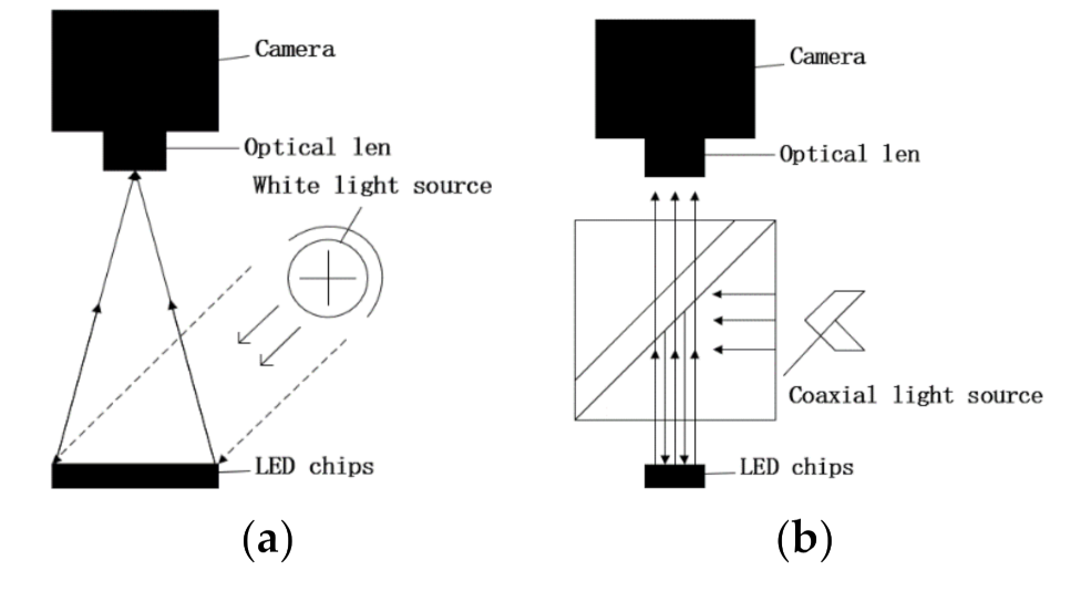
2. Image Acquisition System
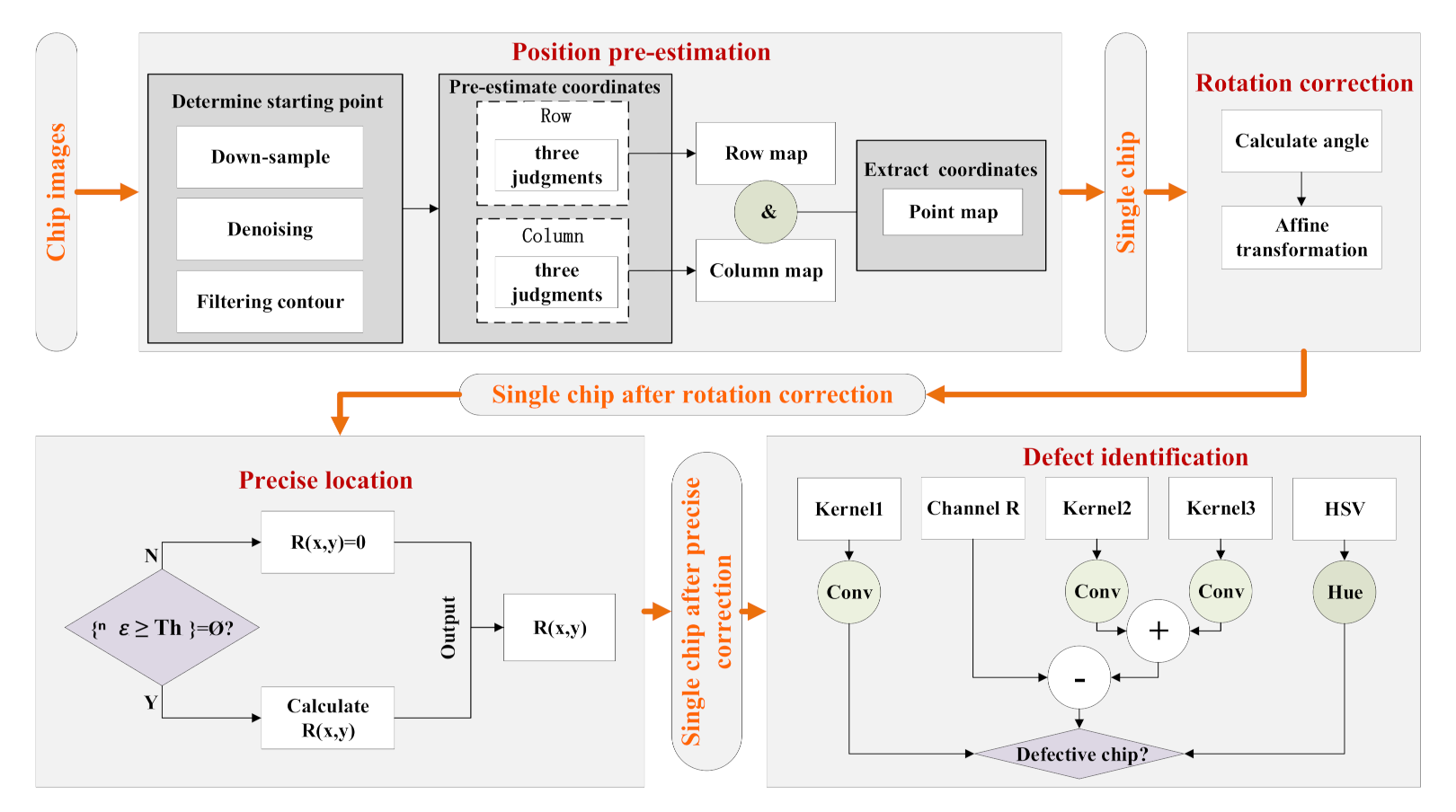
The acquisition of images is the key for a vision system. Since image is the only processing object, the quality of the acquisition system determines the complexity of subsequent image processing algorithms. A reasonable acquisition system is conducive to obtaining an image with high signal–noise ratio and has the characteristic of being insensitive to external light noise. Thus, an acquisition system with resolution of 1.5 μ m / pixel was proposed; the schematic is shown in Figure 2.
During image acquisition, two images were taken from the same location: One was a 24-bit color picture under ring white light source, and the other was an 8-bit grayscale image under coaxial light source. The color picture under ring light simulates the visual of the human eyes, which can replace the work of manual visual inspection after image processing. The coaxial image effectively reflects defects with obvious change in surface roughness, such as electrode pinholes and dry engraving, which cannot be seen through microscope until at a specific lighting angle. The two images were then input into the proposed identification algorithm.

3. Proposed Method

A picture contains hundreds of LED chips, so that segmentation is performed first, and then detection. As shown in Figure 3, the surface defect detection method was carried out by the following steps:
  • Pre-estimate all the coordinates of possible chips in the entire picture;
  • Rotation correction is performed to ensure the accuracy of subsequent precise location and reduce misjudgments;
  • Developing modified NCC algorithm to locate chips precisely to eliminate the influence of brightness changes;
  • Element identification is applied by dividing the LED chip into multiple areas according to its composition (such as electrode area, light-emitting area, etc.).

3.1. Position Pre-Estimation

In the collected chip images, there are large-area vacancies, damages, and irregular arrangements that interfere with chip segmentation. For this, an algorithm based on pre-estimating coordinate was designed to pre-mark all possible chips that may exist in the picture.

3.1.1. Determination of Pre-Estimated Starting Point

To obtain all the possible chip positions, it is necessary to find the starting point of the row and column, respectively, and then calculate the remaining positions. First, a segmentation channel was selected for down-sampling to improve calculation efficiency. Through Formula (1) to connect two adjacent chips, and then Formula (2) to remove burr, the whole picture was divided into several equal parts to avoid the influence of full line tilt. Searching and then filtering contour by width and height, those coordinates of qualified contour were chosen as pre-estimated starting point.
f k = f k k  
f k = f k k  
f k x , y = min s , t k f x + s , y + t
f k x , y = max s , t k f x s , y t
where f is the initial image, and k is structural element.

3.1.2. Pre-Estimate Coordinates

To obtain all possible row and column coordinates, the following three judgments were made:
S P s = s p 1 , s p 2 , , s p n  
Judgment 1: Whether there is a chip before the first pre-estimated starting point. In Formula (5), SPs are the coordinates of qualified contour, and D is the distance between two adjacent chips, so PTs1 is the possible coordinates calculated.
P T s 1 = p t | p t = s p 1 D × N k , k 0 , N 1  
N 1 = s p 1 D  
Judgment 2: Whether there is a chip between the pre-estimated starting points. PTs2 is the possible coordinates calculated.
P T s 2 = p t | p t = s p i + D × k + 1 , k 0 , N 2  
N 2 = s p i + 1 s p i D , i 1 , n  
Judgment 3: Whether there is a chip from the last pre-estimated starting point to the edge of the picture. PTs3 is the possible coordinates calculated. In Formula (11), SZ is the size of the picture.
P T s 3 = p t | p t = s p n + D × k + 1 , k 0 , N 3  
N 3 = S Z s p n D  
By combining the possible coordinates calculated and SPs to obtain all the pre-estimated coordinates:
R e s u l t = S P s P T s 1 P T s 2 P T s 3  

3.1.3. Extract Pre-Estimated Coordinates

By drawing a single-pixel line for each pre-estimated coordinate, a row coordinate map was obtained, as shown in Figure 4b; similarly the column coordinate map was obtained, as shown in Figure 4c.
As shown in Figure 4b,c, the white lines indicate possible row and column coordinates where chips may exist. The ‘AND’ operator was performed on the two coordinate maps to obtain the final pre-estimated point map, as shown in Figure 4d, where each point represents a chip and refers to the center of the chip. Comparing Figure 4a,d, there is no chip distributed in the upper left and the top right of Figure 4a, but the location information is estimated in Figure 4d. It can be seen from the analysis that this method can effectively reduce the influence of chip adhesion and large-area damage during chip segmentation.

3.2. Rotation Correction

After position pre-estimation, a single LED chip was acquired but it was usually inclined. To increase the accuracy of subsequent precise location and reduce misidentification at the same time, angle calculation and affine transformation were performed. By finding the smallest circumscribed rectangle, the inclination Theta angle was obtained according to the four sides of the rectangle. The transformation formula for rotation is defined as follows:
x y = cos θ sin θ sin θ cos θ x y  
where x and y are original coordinates, θ is the angle of rotation, and so x′ and y′ are the coordinates after rotation. The corrected picture is more conducive to machine vision inspection, which can effectively reduce misjudgment and improve detection accuracy.

3.3. Precise Location

After rotation correction, precise location was performed. However, owing to the influence of the production process, the quality of the same chip in different batches varies greatly. Moreover, the changes in ambient light and brightness also increase the difficulty. Based on the above considerations, the NCC algorithm was selected, but it was difficult to be applied online due to its huge amount of computation and slow speed. To this end, a modified NCC algorithm was proposed.

3.3.1. Generation of Template Image

As the same type of chip from different batches also varies a lot in appearance, it is difficult to directly cut out the standard chip from the photographed image. By analyzing the gray level and contours of the chip image, two template images corresponding to the color and coaxial pictures were generated, as shown in Figure 5a,b.

3.3.2. Modified NCC Matching Algorithm

The computational complexity for traditional NCC is O M m × N n × m × n , where M, N is the size of the image to be matched and m, n is the size of the template. There is a huge calculation and computing resources cost when inputting a large image. In order to save computing resources and realize online defect detection, a modified NCC algorithm was carried out according to the following equations:
ε x , y , i , j = f x + i , y + j f   ¯ w i , j w   ¯
f   ¯ = 1 m × n s = 1 m 1 t = 1 n 1 f x + s , y + t
w   ¯ = 1 m × n s = 0 m 1 t = 0 n 1 w s , t
if:
H | min 1 H N u m t h h = 1 H ε x , y , i , j T h
R x , y = 0  
or else:
R x , y = i = 0 m 1 j = 0 n 1 f x + i , y + j f   ¯ × w i , j w ¯ i = 0 m 1 j = 0 n 1 f x + i , y + j f   ¯ 2 × i = 0 m 1 j = 0 n 1 w i , j w   ¯ 2  
where w is a template with the size of   m × n , f is the test picture to be matched, f   ¯ , w   ¯ are the average values of the sub-image and template, respectively, R is a matrix consisting of normalized cross-correlation value, NumTh is set as the threshold for the number of pixels, Th is set as the error threshold, ε is the absolute error of a pixel randomly selected in the sub-image, and so H is the minimum number of pixels with the sum of absolute errors exceeding Th in the sub-image. As shown in Figure 6, the two thresholds Th and NumTh divide the space into four blocks; only the curve passing through block 4 needs further calculation.
It can be seen from the formula that when the similarity is poor, the matching process is ended early, which reduces the calculation for subsequent pixels. It is equivalent to having a rough match first, so that the matching result is the same as the traditional NCC. Additionally, since the average value is subtracted, both the test picture and the template are standardized, which means that the result will not be affected by the change in light intensity. The matching results are shown in Figure 7c,d, where the brighter the result, the better the match. Finally, the coordinate of the maximum value was selected as the precise location result.

3.4. Defect Identification

In order to achieve rapid expansion of chip and defect types, while ensuring the quality of recognition, element identification was proposed. Specifically, the LED chip was first divided into multiple areas according to the composition such as electrode area, light-emitting area, etc. Different feature enhancement schemes were used in these areas. In this study, the main types of defects detected were electrode pinhole missing, conductive-hole exposing, marker-chip recognition, and other detection results.

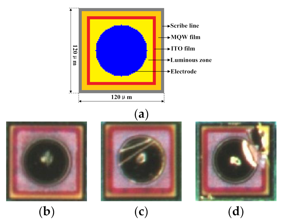
3.4.1. Electrode Pinhole Missing

The existence of electrode pinholes reflects whether the chip has undergone previous electrical tests. Due to the fluctuations of the material tray, the depth of pinholes is inconsistent, as shown in Figure 8a, where shallow electrode pinholes are difficult to identify. In this study, a pinhole-enhanced scheme was designed to increase pinhole’s contrast with the surroundings.
K e r n e l = 0 0 1 0 0 0 1 1 1 0 1 1 12 1 1 0 1 1 1 0 0 0 1 0 0
In order to extract features, the coaxial layer was down-sampled first to amplify dark spots, and then convolved with the designed kernel to suppress noise. The kernel was designed with the feature that the sum of all elements is zero, which can enhance black spots on white background. The result is shown in Figure 8b; pinholes could be extracted through threshold as the gray value of non-pinhole area became almost zero after convolution.

3.4.2. Conductive-Hole Exposing

As shown in Figure 9a, with a small size of 5 μm (3 pixels) and low contrast with the surroundings, conductive-hole exposing appears in batches, which greatly affects the chip yield. Therefore, this has always been a problem for enterprises. To this end, a defect enhancement method was designed, and the counting processes were as follows:
K e r n e l 2 = 1 1 0 2 2 0 1 1 0         1 2 1 2 4 2 1 2 1         0 1 1 0 2 2 0 1 1 × 1 8 ,
K e r n e l 3 = K e r n e l 2 ,
D s t 1 = R     K e r n e l 2 ,
D s t 2 = R     K e r n e l 3 ,
D s t = R D s t 1 + D s t 2 .
where R is the red channel of color image, Kernel2 is the convolution kernel designed after observing characteristics such as size and its comparison with the surroundings, Kernel2′ is the transposed matrix of Kernel2, and ⊗ represents convolution. As the defect occurred around the chip, Dst1 and Dst2 respectively reflected the contrast between the horizontal and vertical directions with the surroundings, as shown in Figure 9b,c. By superimposing the two filtered pictures and subtracting from R, the characteristics were enhanced, and the results after marking are shown in Figure 9d.

3.4.3. Results of Other Defect Categories

Following steps such as grayscale extraction, Sobel gradient, and connected component analysis, etc., identification of red pollution in luminous zone, electrode scratch, corner cracks, ink dots, dry engraving, and twins were realized. The results are shown in Figure 10.

4. Discussion

4.1. Matching Algorithm Comparison Statistics

Compared to traditional NCC and Sequential Similiarity Detection Algorithm (SSDA), Figure 11 shows the matching time and accuracy of five chips in use of the three methods. It can be seen from the data in Figure 11 that the modified NCC algorithm greatly improves the matching speed by eight times while ensuring the accuracy remains the same as the traditional NCC. Although the matching speed of SSDA is the fastest among the three, its accuracy is the lowest.

4.2. Inspection Quality Statistics

A total of 120 sets of pictures containing various defects were selected. Each set included color and corresponding coaxial images. The size of the pictures was 2572 pixels × 1200 pixels, and each picture contained approximately 200 LED chips. The results were measured by True Negative (TN): the number of correctly classified defective chips, True Positive (TP): the number of correctly classified defect-free chips, False Positive (FP): the number of misclassified defect-free chips, and False Negative (FN): the number of misclassified defective chips. It can be drawn from Table 1 that the average TN rate was 99.54% while the FP rate was 0.03%. Due to the use of element recognition, the inspection area covered the entire chip, so that the TP rate was high.
T N r a t e = T N N u m b e r   o f   t o t a l   d e f e c t s  
F P r a t e = F P N u m b e r   o f   d e f e c t f r e e   c h i p s  
T P = ( T o t a l   d e f e c t - f r e e )   F P
F N = ( T o t a l   d e f e c t ) T N

4.3. Inspection Time Statistics

A total of 320 sets of chip pictures with the same type from different batches were randomly selected and divided into four groups, each with 80 sets for testing. The test time included chip position pre-estimation, rotation correction, precise location, and defect identification. The computer configuration was as follows: Win 10, E5-2683 V4 processor with a main frequency of 2.10 GHz, 32 GB memory, and codes were programmed in Visual Studio 2019(Visual C++). The result is presented in Table 2. It can be concluded that the average inspection time of each LED chip was 1.098 ms, which meets the online inspection efficiency requirements of companies. During the chip inspection, inspection time was mainly spent on segmentation and positioning. The position pre-estimation in this study reduced the segmentation time, thereby improving the overall inspection efficiency.

4.4. Compared to Other Methods

Five other mainstream detection methods were also performed and compared in this study; the dataset was the same 320 sets of pictures, and the results are shown in Table 3. It is clear that the method proposed is far more superior in terms of efficiency and accuracy.

5. Conclusions and Suggestions

A chip segmentation method based on position pre-estimation and a modified NCC algorithm, as well as feature enhancement methods are proposed in this study. The segmentation method effectively avoids the interference of chip adhesion, disorderly arrangement, and large area missing. By developing modified NCC matching, the precise location result was not affected by brightness change in acquired pictures. Feature enhancement schemes were designed to separate low-contrast defects quickly and accurately.
The results of the three experiments show that the average accuracy reaches 99.54% while inspection missing rate is 0.03%. In addition, detection time of a single chip is about 1.098 ms, and the smallest defect that can be detected is 2 µm. After performing and comparing to the other five mainstream detection methods, it can be concluded that the proposed method is far more superior in terms of efficiency and accuracy. The work in this study can be used as the algorithm part of the Automated Optical Inspection (AOI) equipment to replace manual surface defect detection of LED chips.
However, template pictures and chip sizes were obtained manually, which can be further improved. At present, the authors’ laboratory has realized the automatic acquisition of chip size and interval. To address this limitation, combining these two programs and exploring how to achieve the automatic generation of templates will be left for future work.

Author Contributions

Conceptualization, L.X. and X.H.; methodology, L.X.; software, L.X. and J.Z.; validation, L.X.; formal analysis, L.X.; investigation, L.X. and J.Z.; resources, L.X.; data curation, L.X. and T.H.; writing—original draft preparation, L.X.; writing—review and editing, L.X. and K.H.; visualization, L.X. and K.H.; supervision, L.X. and X.H. All authors have read and agreed to the published version of the manuscript.

Funding

This research was funded by Characteristic Innovation Projects of Colleges and Universities of Guangdong Province, China, grant number 2021KTSCX111; Shenzhen Pingshan District Science and Technology Innovation Project, Guangdong, China, grant number PSKG202006; Self-made experimental instruments and equipment project of Shenzhen Technology University in 2021 Guangdong, China, grant number 2021015777701059.

Institutional Review Board Statement

Not applicable.

Informed Consent Statement

Not applicable.

Conflicts of Interest

The authors declare no conflict of interest. The funders had no role in the design of the study; in the collection, analyses, or interpretation of data; in the writing of the manuscript; or in the decision to publish the results.

References

  1. Fu, Y.; Ma, X.; Zhou, H. Automatic Detection of Multi-Crossing Crack Defects in Multi-Crystalline Solar Cells Based on Machine Vision. Mach. Vis. Appl. 2021, 32, 60. [Google Scholar] [CrossRef]
  2. Ding, W.; Wang, Q.; Zhu, J. Automatic Detection of Dispersed Defects in Resin Eyeglass Based on Machine Vision Technology. IEEE Access 2020, 8, 44661–44670. [Google Scholar] [CrossRef]
  3. Wu, W.; Li, Q. Machine Vision Inspection of Electrical Connectors Based on Improved Yolo V3. IEEE Access 2020, 8, 166184–166196. [Google Scholar] [CrossRef]
  4. Li, Z.; Zhong, P.; Tang, X.; Chen, Y.; Su, S.; Zhai, T. A New Method to Evaluate Yarn Appearance Qualities Based on Machine Vision and Image Processing. IEEE Access 2020, 8, 30928–30937. [Google Scholar] [CrossRef]
  5. Luo, Q.; Fang, X.; Liu, L.; Yang, C.; Sun, Y. Automated Visual Defect Detection for Flat Steel Surface: A Survey. IEEE Trans. Instrum. Meas. 2020, 69, 626–644. [Google Scholar] [CrossRef] [Green Version]
  6. Czimmermann, T.; Ciuti, G.; Milazzo, M.; Chiurazzi, M.; Roccella, S.; Oddo, C.M.; Dario, P. Visual-Based Defect Detection and Classification Approaches for Industrial Applications—A Survey. Sensors 2020, 20, 1459. [Google Scholar] [CrossRef] [Green Version]
  7. Stefenon, S.F.; Dal Molin Ribeiro, M.H.; Nied, A.; Mariani, V.C.; dos Santos Coelho, L.; Menegat da Rocha, D.F.; Grebogi, R.B.; de Barros Ruano, A.E. Wavelet Group Method of Data Handling for Fault Prediction in Electrical Power Insulators. Int. J. Electr. Power Energy Syst. 2020, 123, 106269. [Google Scholar] [CrossRef]
  8. Frizzo Stefenon, S.; Zanetti Freire, R.; dos Santos Coelho, L.; Meyer, L.H.; Bartnik Grebogi, R.; Gouvêa Buratto, W.; Nied, A. Electrical Insulator Fault Forecasting Based on a Wavelet Neuro-Fuzzy System. Energies 2020, 13, 484. [Google Scholar] [CrossRef] [Green Version]
  9. Zhang, H.; Sun, H.; Shi, P. Chip Appearance Inspection Method for High-Precision SMT Equipment. Machines 2021, 9, 34. [Google Scholar] [CrossRef]
  10. Sun, H.; Yang, X.; Gao, H. A Spatially Constrained Shifted Asymmetric Laplace Mixture Model for the Grayscale Image Segmentation. Neurocomputing 2019, 331, 50–57. [Google Scholar] [CrossRef]
  11. Bay, H.; Ess, A.; Tuytelaars, T.; Van Gool, L. Speeded-Up Robust Features (SURF). Comput. Vis. Image Underst. 2008, 110, 346–359. [Google Scholar] [CrossRef]
  12. Liu, X.; Hu, Y. Inspection of IC Wafer Defects Based on Image Registration. In Proceedings of the 2018 IEEE 3rd Advanced Information Technology, Electronic and Automation Control Conference (IAEAC), Chongqing, China, 12–14 October 2018. [Google Scholar]
  13. Lin, B.; Wang, J.; Yang, X.; Tang, Z.; Li, X.; Duan, C.; Zhang, X. Defect Contour Detection of Complex Structural Chips. Math. Probl. Eng. 2021, 2021, 5518675. [Google Scholar] [CrossRef]
  14. Canny, J. A Computational Approach to Edge Detection. IEEE Trans. Pattern Anal. Mach. Intell. 1986, PAMI-8, 679–698. [Google Scholar] [CrossRef]
  15. Chen, X.; Zhao, C.; Chen, J.; Zhang, D.; Zhu, K.; Su, Y. K-Means Clustering with Morphological Filtering for Silicon Wafer Grain Defect Detection. In Proceedings of the 2020 IEEE 4th Information Technology, Networking, Electronic and Automation Control Conference (ITNEC), Chongqing, China, 12–14 June 2020; pp. 1251–1255. [Google Scholar]
  16. Kyeong, K.; Kim, H. Classification of Mixed-Type Defect Patterns in Wafer Bin Maps Using Convolutional Neural Networks. IEEE Trans. Semicond. Manuf. 2018, 31, 395–402. [Google Scholar] [CrossRef]
  17. Nakazawa, T.; Kulkarni, D.V. Wafer Map Defect Pattern Classification and Image Retrieval Using Convolutional Neural Network. IEEE Trans. Semicond. Manuf. 2018, 31, 309–314. [Google Scholar] [CrossRef]
  18. Wang, J.; Xu, C.; Yang, Z.; Zhang, J.; Li, X. Deformable Convolutional Networks for Efficient Mixed-Type Wafer Defect Pattern Recognition. IEEE Trans. Semicond. Manuf. 2020, 33, 587–596. [Google Scholar] [CrossRef]
  19. Chen, S.-H.; Kang, C.-H.; Perng, D.-B. Detecting and Measuring Defects in Wafer Die Using GAN and YOLOv3. Appl. Sci. 2020, 10, 8725. [Google Scholar] [CrossRef]
  20. Chien, J.-C.; Wu, M.-T.; Lee, J.-D. Inspection and Classification of Semiconductor Wafer Surface Defects Using CNN Deep Learning Networks. Appl. Sci. 2020, 10, 5340. [Google Scholar] [CrossRef]
  21. Lin, H.; Li, B.; Wang, X.; Shu, Y.; Niu, S. Automated Defect Inspection of LED Chip Using Deep Convolutional Neural Network. J. Intell. Manuf. 2019, 30, 2525–2534. [Google Scholar] [CrossRef]
  22. Zhou, B.; Khosla, A.; Lapedriza, A.; Oliva, A.; Torralba, A. Learning Deep Features for Discriminative Localization. In Proceedings of the 2016 IEEE Conference on Computer Vision and Pattern Recognition (CVPR), Las Vegas, NV, USA, 27–30 June 2016; pp. 2921–2929. [Google Scholar]
  23. Chen, X.; Chen, J.; Han, X.; Zhao, C.; Zhang, D.; Zhu, K.; Su, Y. A Light-Weighted CNN Model for Wafer Structural Defect Detection. IEEE Access 2020, 8, 24006–24018. [Google Scholar] [CrossRef]
  24. Goodfellow, I.J.; Pouget-Abadie, J.; Mirza, M.; Xu, B.; Warde-Farley, D.; Ozair, S.; Courville, A.; Bengio, Y. Generative Adversarial Networks. arXiv 2014, arXiv:1406.2661. [Google Scholar] [CrossRef]
  25. Redmon, J.; Farhadi, A. YOLOv3: An Incremental Improvement. arXiv 2018, arXiv:1804.02767. [Google Scholar]
  26. Chen, S.-H.; Tsai, C.-C. SMD LED Chips Defect Detection Using a YOLOv3-Dense Model. Adv. Eng. Inform. 2021, 47, 101255. [Google Scholar] [CrossRef]
Figure 1. Examples of LED chips: (a) sketch of chip; (b) normal chip; (c) chip with scratches; (d) chip with crack.
Applsci 12 01265 g001
Figure 2. Schematic diagram of image acquisition system: (a) color image acquisition system; (b) coaxial image acquisition system.
Applsci 12 01265 g002
Figure 3. Process of defect detection.
Applsci 12 01265 g003
Figure 4. Results in the process of pre-estimating position: (a) original picture; (b) row coordinate map; (c) column coordinate map; (d) pre-estimated point map.
Applsci 12 01265 g004
Figure 5. Chip template: (a) template for color picture; (b) template for coaxial picture.
Applsci 12 01265 g005
Figure 6. Illustration of the condition.
Applsci 12 01265 g006
Figure 7. Modified NCC matching result: (a) color area to be matched; (b) coaxial area to be matched; (c) color area matching result; (d) coaxial area matching result.
Applsci 12 01265 g007
Figure 8. Electrode-pinhole-missing: (a) shallow pinhole; (b) extracting.
Applsci 12 01265 g008
Figure 9. Conductive-hole exposing: (a) initial picture; (b) convolution Dst1; (c) convolution Dst2; (d) extracting.
Applsci 12 01265 g009
Figure 10. Results of other defect categories: (a) red pollution; (b) scratch; (c) corner crack; (d) ink dots; (e) dry engraving; (f) twins.
Applsci 12 01265 g010
Figure 11. Performance of the modified NCC in matching time and accuracy.
Applsci 12 01265 g011
Table 1. Inspection quality statistics.
Defect TypeTotal Defect-FreeTotal DefectsTNTN Rate (%)FPFP Rate (%)
Corner crack19,73617917910000
Scratch19,73632432199.0720.01
Pinhole missing19,73637137110000
Ink dots19,73623723710000
Twins19,73624624610000
Dry engraving19,73652752399.2430.01
Conductive-hole exposing19,73635935799.4400
Red pollution in luminous zone19,73637837599.2120.01
Table 2. Inspection time statistics.
GroupTotal Time (ms)Average Time of Single Image (ms)Average Time of Single Chip (ms)
Group one17,852.475223.1561.116
Group two17,313.364216.4171.082
Group three17,833.533221.9191.110
Group four17,349.067216.8631.084
Average17,587.110219.5891.098
Table 3. Comparison to other method.
MethodsImage Size (Pixels)Average Time of Single Chip (ms)Accuracy (%)
DWPD [9] 1028 × 1024 - 93
Registration with Canny [13] 204 × 146 44.0897.27
CNN [20] 256 × 256 32098.88
LED-Net [21] 227 × 227 14.8894.96
YOLOv3-dense [26] 416 × 416 2995.28
Our Method 2572 × 1200 1.09899.54
Publisher’s Note: MDPI stays neutral with regard to jurisdictional claims in published maps and institutional affiliations.

