Defect Detection on LED Chips Based on Position Pre-Estimation and Feature Enhancement
Abstract
:1. Introduction
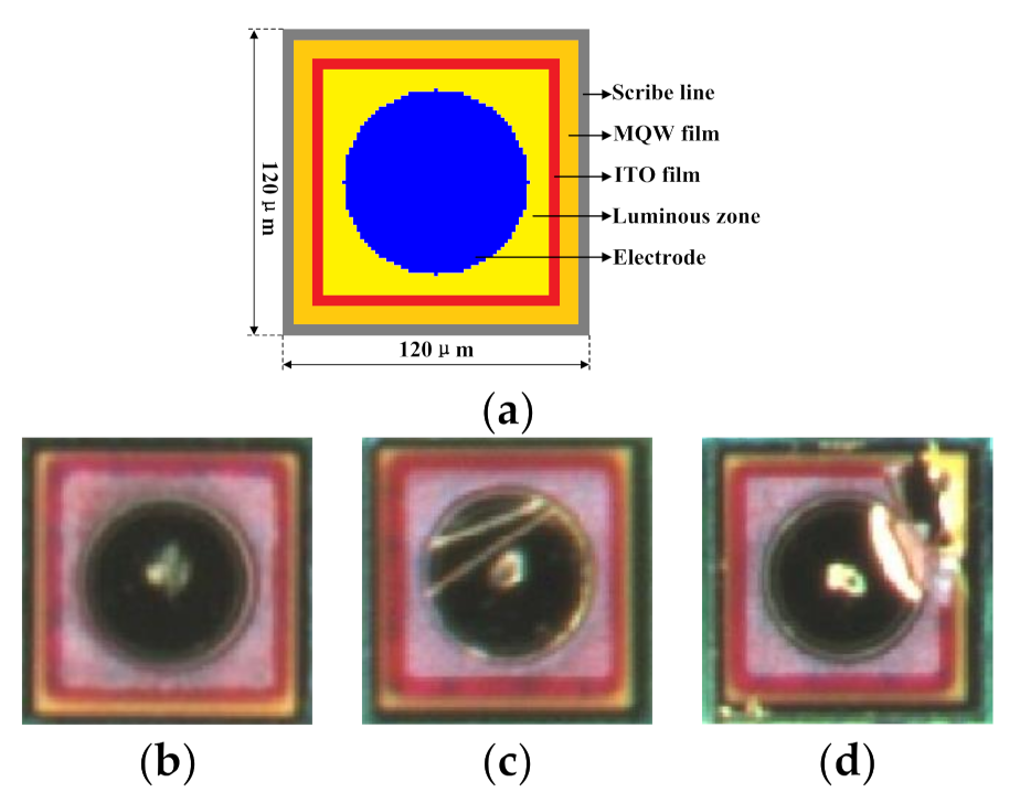
- Difficult to locate position of the defect accurately.
- Irregular defect shape increases image annotation time.
- Poor versatility and portability for different batches and types of products.
- Long training time, expensive calculation, and difficulty in collecting training samples; When the defect standard changes, training needs to be carried out from scratch, which cannot meet the production timeliness required by the enterprise.
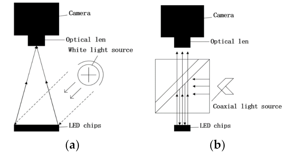
2. Image Acquisition System
3. Proposed Method
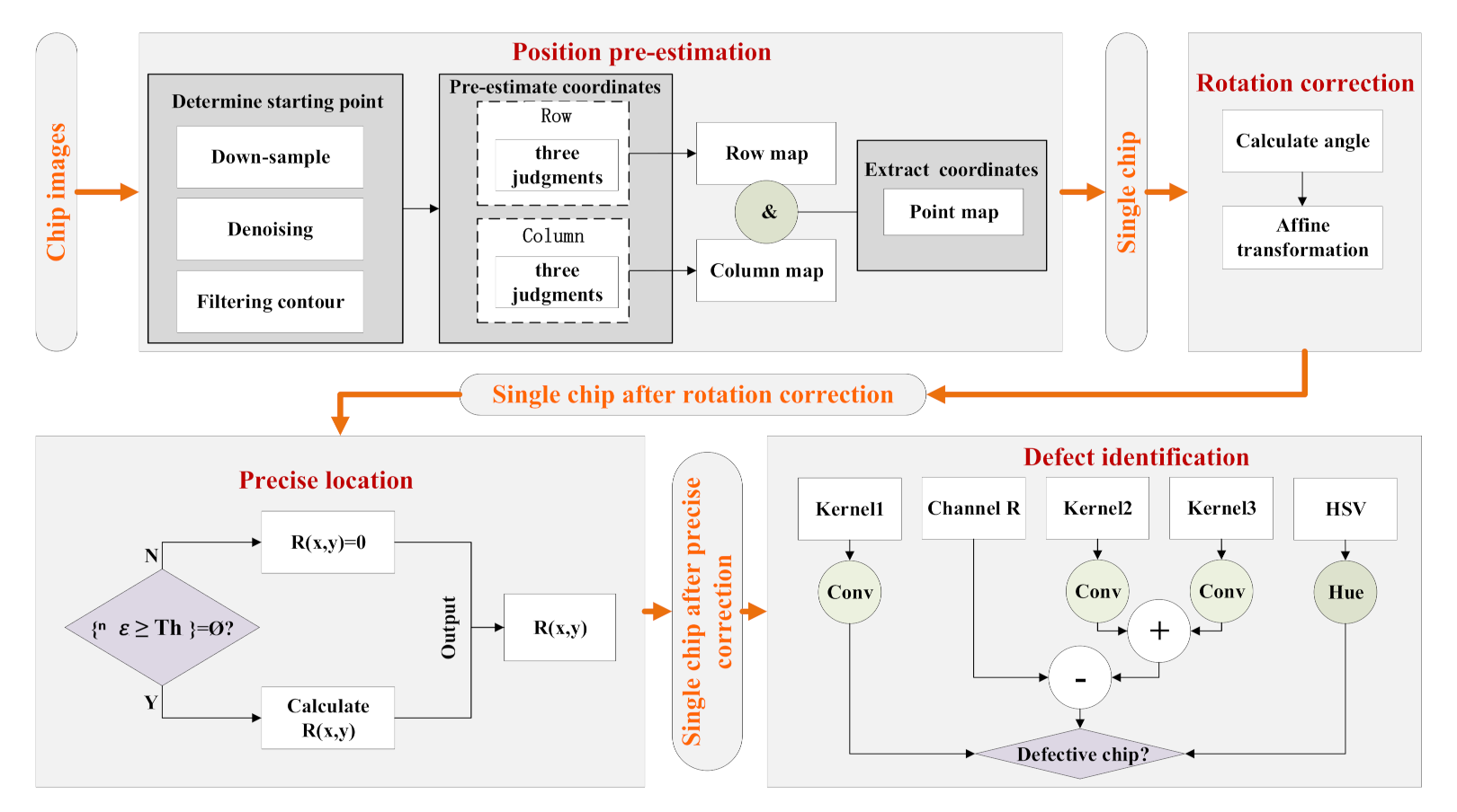
- Pre-estimate all the coordinates of possible chips in the entire picture;
- Rotation correction is performed to ensure the accuracy of subsequent precise location and reduce misjudgments;
- Developing modified NCC algorithm to locate chips precisely to eliminate the influence of brightness changes;
- Element identification is applied by dividing the LED chip into multiple areas according to its composition (such as electrode area, light-emitting area, etc.).
3.1. Position Pre-Estimation
3.1.1. Determination of Pre-Estimated Starting Point
3.1.2. Pre-Estimate Coordinates
3.1.3. Extract Pre-Estimated Coordinates
3.2. Rotation Correction
3.3. Precise Location
3.3.1. Generation of Template Image
3.3.2. Modified NCC Matching Algorithm
3.4. Defect Identification
3.4.1. Electrode Pinhole Missing
3.4.2. Conductive-Hole Exposing
3.4.3. Results of Other Defect Categories
4. Discussion
4.1. Matching Algorithm Comparison Statistics
4.2. Inspection Quality Statistics
4.3. Inspection Time Statistics
4.4. Compared to Other Methods
5. Conclusions and Suggestions
Author Contributions
Funding
Institutional Review Board Statement
Informed Consent Statement
Conflicts of Interest
References
- Fu, Y.; Ma, X.; Zhou, H. Automatic Detection of Multi-Crossing Crack Defects in Multi-Crystalline Solar Cells Based on Machine Vision. Mach. Vis. Appl. 2021, 32, 60. [Google Scholar] [CrossRef]
- Ding, W.; Wang, Q.; Zhu, J. Automatic Detection of Dispersed Defects in Resin Eyeglass Based on Machine Vision Technology. IEEE Access 2020, 8, 44661–44670. [Google Scholar] [CrossRef]
- Wu, W.; Li, Q. Machine Vision Inspection of Electrical Connectors Based on Improved Yolo V3. IEEE Access 2020, 8, 166184–166196. [Google Scholar] [CrossRef]
- Li, Z.; Zhong, P.; Tang, X.; Chen, Y.; Su, S.; Zhai, T. A New Method to Evaluate Yarn Appearance Qualities Based on Machine Vision and Image Processing. IEEE Access 2020, 8, 30928–30937. [Google Scholar] [CrossRef]
- Luo, Q.; Fang, X.; Liu, L.; Yang, C.; Sun, Y. Automated Visual Defect Detection for Flat Steel Surface: A Survey. IEEE Trans. Instrum. Meas. 2020, 69, 626–644. [Google Scholar] [CrossRef] [Green Version]
- Czimmermann, T.; Ciuti, G.; Milazzo, M.; Chiurazzi, M.; Roccella, S.; Oddo, C.M.; Dario, P. Visual-Based Defect Detection and Classification Approaches for Industrial Applications—A Survey. Sensors 2020, 20, 1459. [Google Scholar] [CrossRef] [Green Version]
- Stefenon, S.F.; Dal Molin Ribeiro, M.H.; Nied, A.; Mariani, V.C.; dos Santos Coelho, L.; Menegat da Rocha, D.F.; Grebogi, R.B.; de Barros Ruano, A.E. Wavelet Group Method of Data Handling for Fault Prediction in Electrical Power Insulators. Int. J. Electr. Power Energy Syst. 2020, 123, 106269. [Google Scholar] [CrossRef]
- Frizzo Stefenon, S.; Zanetti Freire, R.; dos Santos Coelho, L.; Meyer, L.H.; Bartnik Grebogi, R.; Gouvêa Buratto, W.; Nied, A. Electrical Insulator Fault Forecasting Based on a Wavelet Neuro-Fuzzy System. Energies 2020, 13, 484. [Google Scholar] [CrossRef] [Green Version]
- Zhang, H.; Sun, H.; Shi, P. Chip Appearance Inspection Method for High-Precision SMT Equipment. Machines 2021, 9, 34. [Google Scholar] [CrossRef]
- Sun, H.; Yang, X.; Gao, H. A Spatially Constrained Shifted Asymmetric Laplace Mixture Model for the Grayscale Image Segmentation. Neurocomputing 2019, 331, 50–57. [Google Scholar] [CrossRef]
- Bay, H.; Ess, A.; Tuytelaars, T.; Van Gool, L. Speeded-Up Robust Features (SURF). Comput. Vis. Image Underst. 2008, 110, 346–359. [Google Scholar] [CrossRef]
- Liu, X.; Hu, Y. Inspection of IC Wafer Defects Based on Image Registration. In Proceedings of the 2018 IEEE 3rd Advanced Information Technology, Electronic and Automation Control Conference (IAEAC), Chongqing, China, 12–14 October 2018. [Google Scholar]
- Lin, B.; Wang, J.; Yang, X.; Tang, Z.; Li, X.; Duan, C.; Zhang, X. Defect Contour Detection of Complex Structural Chips. Math. Probl. Eng. 2021, 2021, 5518675. [Google Scholar] [CrossRef]
- Canny, J. A Computational Approach to Edge Detection. IEEE Trans. Pattern Anal. Mach. Intell. 1986, PAMI-8, 679–698. [Google Scholar] [CrossRef]
- Chen, X.; Zhao, C.; Chen, J.; Zhang, D.; Zhu, K.; Su, Y. K-Means Clustering with Morphological Filtering for Silicon Wafer Grain Defect Detection. In Proceedings of the 2020 IEEE 4th Information Technology, Networking, Electronic and Automation Control Conference (ITNEC), Chongqing, China, 12–14 June 2020; pp. 1251–1255. [Google Scholar]
- Kyeong, K.; Kim, H. Classification of Mixed-Type Defect Patterns in Wafer Bin Maps Using Convolutional Neural Networks. IEEE Trans. Semicond. Manuf. 2018, 31, 395–402. [Google Scholar] [CrossRef]
- Nakazawa, T.; Kulkarni, D.V. Wafer Map Defect Pattern Classification and Image Retrieval Using Convolutional Neural Network. IEEE Trans. Semicond. Manuf. 2018, 31, 309–314. [Google Scholar] [CrossRef]
- Wang, J.; Xu, C.; Yang, Z.; Zhang, J.; Li, X. Deformable Convolutional Networks for Efficient Mixed-Type Wafer Defect Pattern Recognition. IEEE Trans. Semicond. Manuf. 2020, 33, 587–596. [Google Scholar] [CrossRef]
- Chen, S.-H.; Kang, C.-H.; Perng, D.-B. Detecting and Measuring Defects in Wafer Die Using GAN and YOLOv3. Appl. Sci. 2020, 10, 8725. [Google Scholar] [CrossRef]
- Chien, J.-C.; Wu, M.-T.; Lee, J.-D. Inspection and Classification of Semiconductor Wafer Surface Defects Using CNN Deep Learning Networks. Appl. Sci. 2020, 10, 5340. [Google Scholar] [CrossRef]
- Lin, H.; Li, B.; Wang, X.; Shu, Y.; Niu, S. Automated Defect Inspection of LED Chip Using Deep Convolutional Neural Network. J. Intell. Manuf. 2019, 30, 2525–2534. [Google Scholar] [CrossRef]
- Zhou, B.; Khosla, A.; Lapedriza, A.; Oliva, A.; Torralba, A. Learning Deep Features for Discriminative Localization. In Proceedings of the 2016 IEEE Conference on Computer Vision and Pattern Recognition (CVPR), Las Vegas, NV, USA, 27–30 June 2016; pp. 2921–2929. [Google Scholar]
- Chen, X.; Chen, J.; Han, X.; Zhao, C.; Zhang, D.; Zhu, K.; Su, Y. A Light-Weighted CNN Model for Wafer Structural Defect Detection. IEEE Access 2020, 8, 24006–24018. [Google Scholar] [CrossRef]
- Goodfellow, I.J.; Pouget-Abadie, J.; Mirza, M.; Xu, B.; Warde-Farley, D.; Ozair, S.; Courville, A.; Bengio, Y. Generative Adversarial Networks. arXiv 2014, arXiv:1406.2661. [Google Scholar] [CrossRef]
- Redmon, J.; Farhadi, A. YOLOv3: An Incremental Improvement. arXiv 2018, arXiv:1804.02767. [Google Scholar]
- Chen, S.-H.; Tsai, C.-C. SMD LED Chips Defect Detection Using a YOLOv3-Dense Model. Adv. Eng. Inform. 2021, 47, 101255. [Google Scholar] [CrossRef]


| Defect Type | Total Defect-Free | Total Defects | TN | TN Rate (%) | FP | FP Rate (%) |
|---|---|---|---|---|---|---|
| Corner crack | 19,736 | 179 | 179 | 100 | 0 | 0 |
| Scratch | 19,736 | 324 | 321 | 99.07 | 2 | 0.01 |
| Pinhole missing | 19,736 | 371 | 371 | 100 | 0 | 0 |
| Ink dots | 19,736 | 237 | 237 | 100 | 0 | 0 |
| Twins | 19,736 | 246 | 246 | 100 | 0 | 0 |
| Dry engraving | 19,736 | 527 | 523 | 99.24 | 3 | 0.01 |
| Conductive-hole exposing | 19,736 | 359 | 357 | 99.44 | 0 | 0 |
| Red pollution in luminous zone | 19,736 | 378 | 375 | 99.21 | 2 | 0.01 |
| Group | Total Time (ms) | Average Time of Single Image (ms) | Average Time of Single Chip (ms) |
|---|---|---|---|
| Group one | 17,852.475 | 223.156 | 1.116 |
| Group two | 17,313.364 | 216.417 | 1.082 |
| Group three | 17,833.533 | 221.919 | 1.110 |
| Group four | 17,349.067 | 216.863 | 1.084 |
| Average | 17,587.110 | 219.589 | 1.098 |
Publisher’s Note: MDPI stays neutral with regard to jurisdictional claims in published maps and institutional affiliations. |
© 2022 by the authors. Licensee MDPI, Basel, Switzerland. This article is an open access article distributed under the terms and conditions of the Creative Commons Attribution (CC BY) license (https://creativecommons.org/licenses/by/4.0/).
Share and Cite
Xu, L.; Hu, X.; He, T.; Hu, K.; Zhang, J. Defect Detection on LED Chips Based on Position Pre-Estimation and Feature Enhancement. Appl. Sci. 2022, 12, 1265. https://doi.org/10.3390/app12031265
Xu L, Hu X, He T, Hu K, Zhang J. Defect Detection on LED Chips Based on Position Pre-Estimation and Feature Enhancement. Applied Sciences. 2022; 12(3):1265. https://doi.org/10.3390/app12031265
Chicago/Turabian StyleXu, Lu, Xuejuan Hu, Ting He, Kai Hu, and Jaming Zhang. 2022. "Defect Detection on LED Chips Based on Position Pre-Estimation and Feature Enhancement" Applied Sciences 12, no. 3: 1265. https://doi.org/10.3390/app12031265
APA StyleXu, L., Hu, X., He, T., Hu, K., & Zhang, J. (2022). Defect Detection on LED Chips Based on Position Pre-Estimation and Feature Enhancement. Applied Sciences, 12(3), 1265. https://doi.org/10.3390/app12031265


