Article

Operational Stability Analysis of Blue Thermally Activated Delayed Fluorescence Organic Light-Emitting Diodes Using the Capacitance-Voltage Method

Display and Nanosensor Laboratory, Department of Electrical Engineering, Korea University, Seoul 02841, Republic of Korea
*
Author to whom correspondence should be addressed.
Appl. Sci. 2022, 12(24), 13045; https://doi.org/10.3390/app122413045
Submission received: 3 November 2022 / Revised: 25 November 2022 / Accepted: 16 December 2022 / Published: 19 December 2022
(This article belongs to the Section Optics and Lasers)

Abstract

:
We analyzed the degradation features by measuring the capacitance–voltage characteristics after electrically aging blue thermally activated delayed fluorescence (TADF) organic light-emitting diodes (OLEDs). The measurement was investigated in terms of the hole transfer layer (HTL) and electron transfer layer (ETL) structures. For the HTL, three different materials—N,N′–bis(naphthalen–1–yl)–N,N′–bis(phenyl)–benzidine (NPB), 4,4′,4″-tris(carbazol–9–yl)triphenylamine (TCTA), and 1,3–bis(carbazol–9–yl)benzene (mCP)—were used at the HTL/emission layer (EML) interface; the TCTA/EML interface had the highest stability among the interfaces. For the ETL, bis [2–(diphenylphosphino)phenyl] ether oxide (DPEPO) without further dopants was used as an exciton blocking layer (ExBL) to effectively confine the excitons at the EML. However, DPEPO has low stability and carrier mobility. Therefore, 0, 10, and 40 nm-thick ExBL devices were investigated; it was found that the 0 nm-thick ExBL device was the most stable. However, the 10 nm-thick ExBL is essential to confine the excitons at the EML, which ensures a high EL performance.

1. Introduction

Recently, thermally activated delayed fluorescence (TADF) organic light-emitting diodes (OLEDs) have attracted significant research interest because a maximum internal quantum efficiency as high as 100% can be theoretically achieved without the need for rare and heavy metals, such as iridium [1,2,3,4,5]. As the injected holes and electrons recombine, singlet and triplet excitons are formed at a ratio of 1:3 [6,7,8,9]. TADF emitters up-convert triplet excitons into singlet excitons by the reverse intersystem crossing process when the energy split (ΔEST) between the singlet (S1) and triplet (T1) excited states is sufficiently small [10,11].
Blue TADF OLEDs with a maximum external quantum efficiency (EQE) of over 20% have been consistently reported in recent literature [12,13,14]. Although TADF OLEDs have demonstrated high efficiencies, their poor stability is a significant drawback compared to phosphorescent OLEDs. Blue devices can be considered even less stable because they have a shorter lifetime than red or green devices. Many researchers have attempted to address the stability problem by focusing on the lifetime and roll-off characteristics of OLEDs. The approaches detailed in these studies include optimizing the host/dopant ratio and synthesizing new materials for blue TADF emitters [14,15,16,17].
Despite significant efforts to improve the stability of blue TADF OLEDs, there is a paucity of quantitative analyses of their degradation. Measuring J-V and EL characteristics, along with the infrared imaging method, is the most representative OLED degradation characteristic analysis technique; however, it is difficult to analyze the degradation characteristics according to the light-emitting mechanism of OLED. These methods also sometimes prevent the measured OLED pixels from being used again. On the other hand, it is possible to quantitatively analyze the degradation characteristics of the aged device considering the charge accumulation feature at the organic interfaces using C-V characteristics and the Cole-Cole plot [18,19]. In this study, an impedance analyzer, which is non-destructive measuring equipment, was used to investigate the degradation features of blue TADF OLEDs by measuring the capacitance–voltage (C-V) characteristics.
Most triplets and polarons are mainly accumulated at the interface of organic layers due to differences in energy levels and carrier mobility between them; and these cause annihilation and quenching phenomena between excitons and polarons, which are the representative reasons for device degradation. In this study, the hole transfer layer (HTL) structure and thickness of the exciton blocking layer (ExBL) were varied. Both independent variables are adjacent to the emission layer (EML) interface, where most carriers accumulate.

2. Materials and Methods

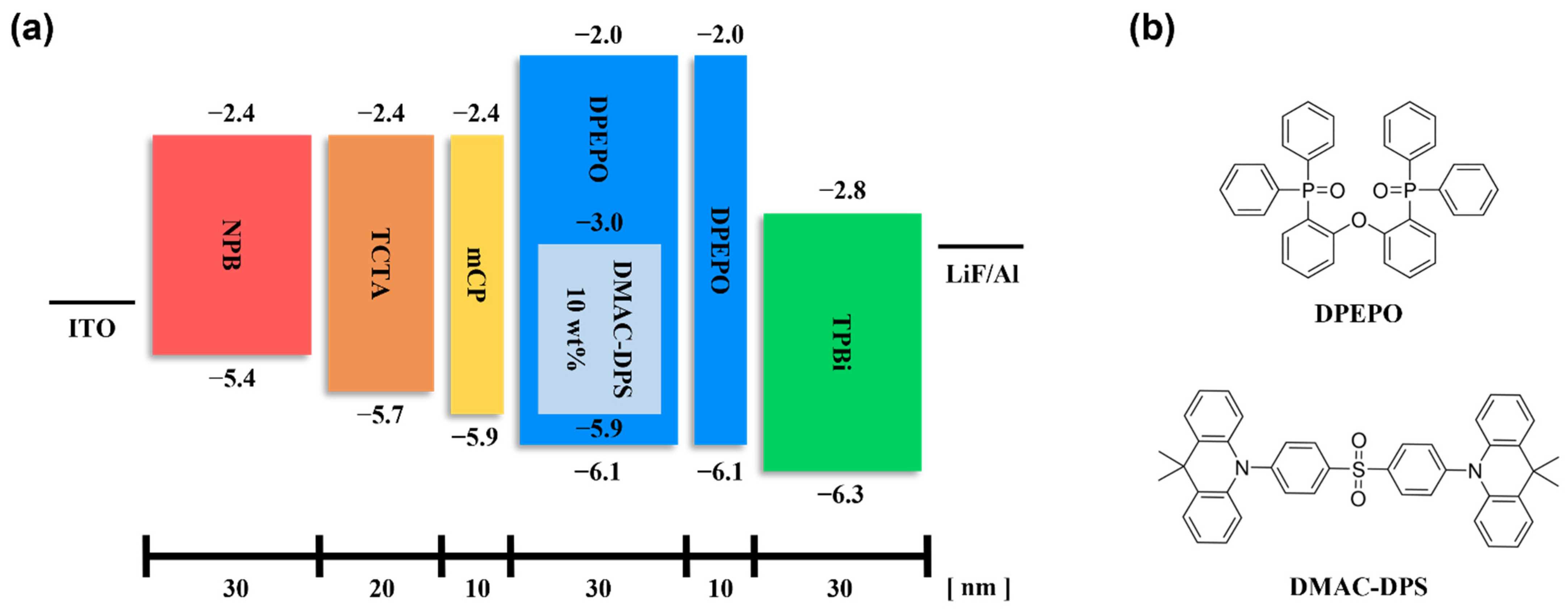
2.1. Device Fabrication and Materials

Figure 1a presents the energy-level diagram and the structure of the blue TADF OLEDs used as the reference (device 1) in this study. The device was fabricated as follows: on an indium tin oxide (ITO) substrate, N,N′–bis(naphthalen–1–yl)–N,N′–bis(phenyl)–benzidine (NPB), 4,4′,4″-tris(carbazol–9–yl)triphenylamine (TCTA), and 1,3–bis(carbazol–9–yl)benzene (mCP) were used as the HTL, and 10 wt% of 10,10′-(4,4′-sulfonylbis(4,1–phenylene))bis(9,9–dimethyl–9,10–dihydroacridine) (DMAC-DPS)-doped bis [2–(diphenylphosphino)phenyl]ether oxide (DPEPO) was used as the EML. The chemical structures of the materials used for the EML are shown in Figure 1b. An additional DPEPO layer without a dopant was used as the ExBL, and 1,3,5–Tris(1–phenyl–1Hbenzimidazol–2–yl)benzene (TPBi) was used as the electron transport layer (ETL). Finally, lithium fluoride (LiF) and aluminum (Al), which were used as the electron injection layer (EIL) and cathode, respectively, were deposited.
Before device fabrication, the ITO-precoated substrate was cleaned in acetone and methanol and rinsed in deionized water with sonication for 10 min. The emitting area, 6.25 mm × 6.25 mm, was fixed by a photoresist layer. The organic materials and metal structures were deposited at rates of 0.5–1 and 1–3 Å/s, respectively, under high-vacuum conditions.
To determine the relationship between the device stability and C-V characteristics, the structure of the OLED was varied in terms of the HTL and ETL, as summarized in Table 1. As devices 1, 2, and 3 demonstrate different HTL/EML interfaces, the degradation characteristics of each HTL layer could be analyzed. For analysis from the ETL perspective, devices 1, 4, and 5 were fabricated, and the thicknesses of the ExBL were set to 10, 0, and 40 nm, respectively.

2.2. Measurement

Impedance spectroscopy has been widely used in the field of organic material-based electronic devices. The degradation of OLEDs was analyzed by measuring the C-V characteristics—a powerful, quantitative, and non-destructive method. The C-V characteristics were measured using an impedance analyzer (E4990A impedance analyzer, Keysight Technologies, Inc., Santa Rosa, USA) with an AC voltage at a frequency of 1 kHz and an amplitude of 100 mV before and after electrical aging.
The electroluminescence (EL) characteristics of the fabricated devices were measured using a spectroradiometer (Spectra Scan PR-670, Photo Research, Inc., North Syracuse, USA) with a Keithley 237 High-Voltage Source-Measure unit (Keithley Instruments, Inc., Cleveland, OH, USA) in a dark box.

3. Results and Discussion

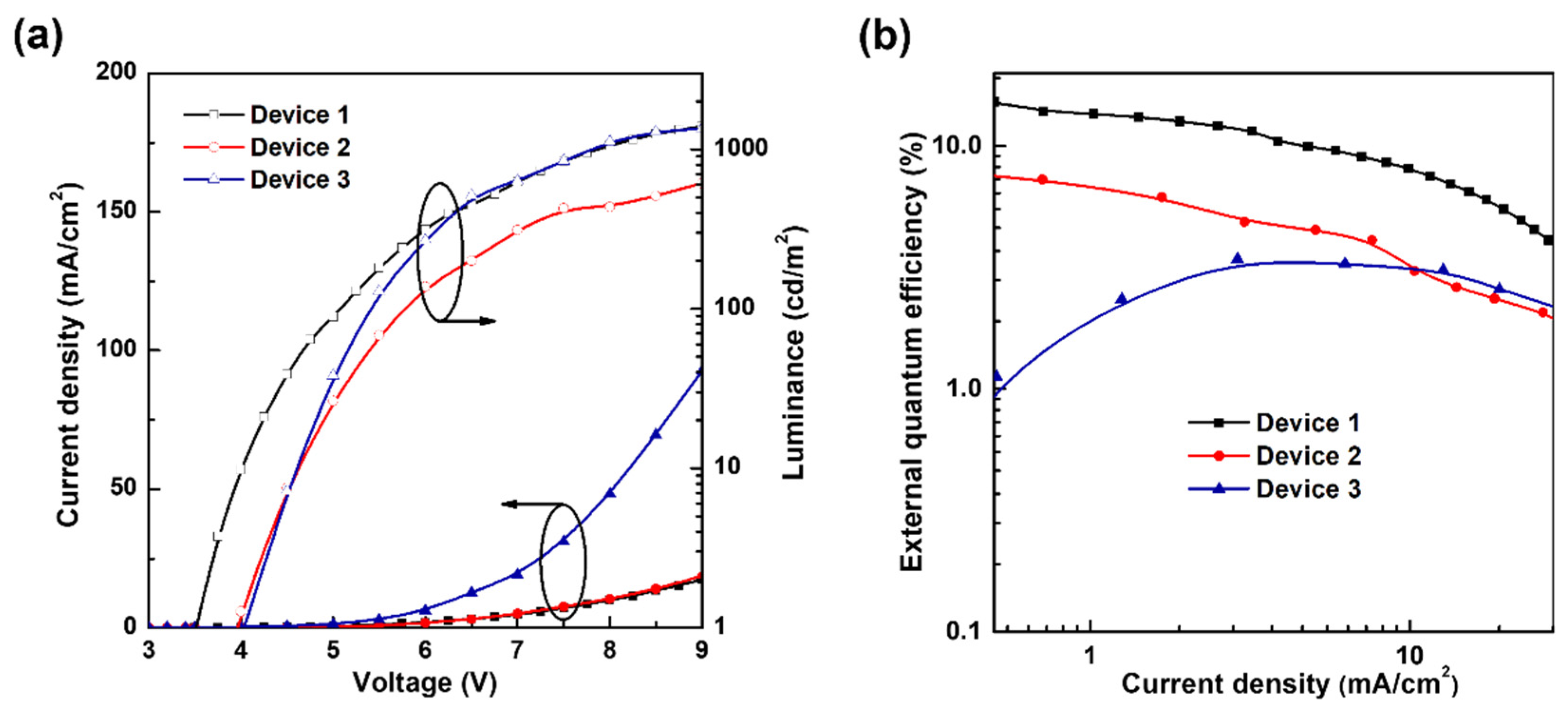
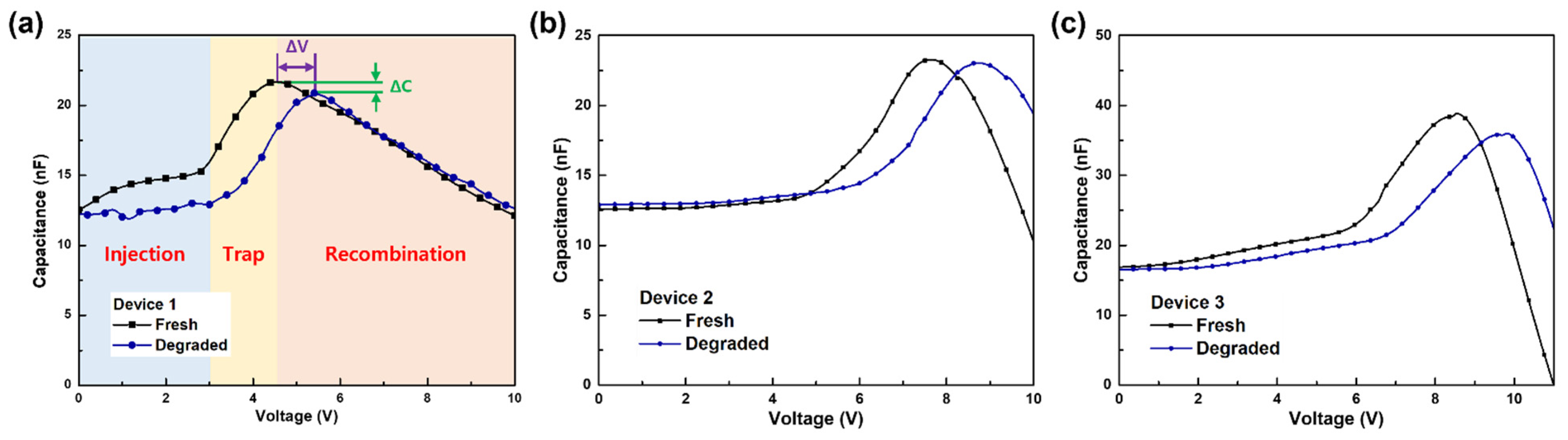
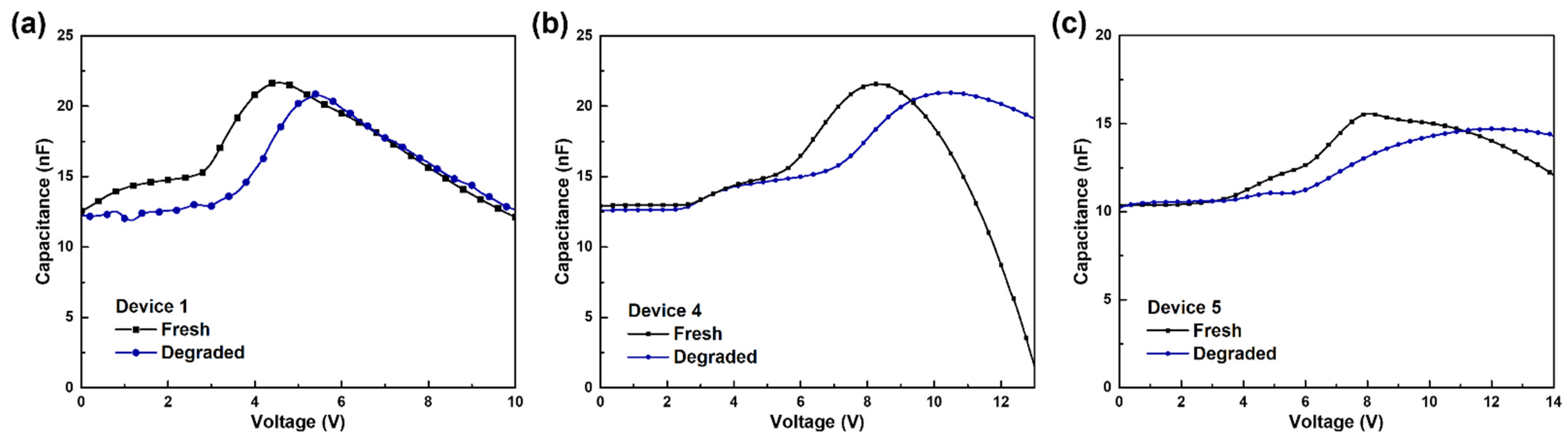
3.1. Analysis of the Degradation of Blue TADF OLEDs by Different HTL Structures

In this section, the operational stability of blue TADF OLEDs with different HTL structures is discussed. Devices 1, 2, and 3 were fabricated, and the neighboring HTLs to the EML were mCP, TCTA, and NPB, respectively. Figure 2 depicts the EL characteristics of undegraded devices 1, 2, and 3, and Table 2 summarizes the performance of each device. Considering the highest occupied molecular orbital energy level of each device’s HTL and DPEPO materials (see Figure 1a), the hole injection barriers of devices 1, 2, and 3 are 0.2, 0.4, and 0.7 eV, respectively. The barrier causes carrier accumulation, which induces a space-charge region and increases the electric potential in the forward bias [20]. Consequently, device 1, with the smallest barrier, exhibits the lowest turn-on voltage. For the same reason, device 2 demonstrates better performance than device 3.
Figure 3 and Table 3 present the C-V characteristics of devices 1, 2, and 3 before and after electrical aging at a current density of 10 mA/cm2 for 10 min. The graphs of the C-V characteristics of the devices are of the same shape; as the voltage increases, the capacitance decreases shortly after a slight increase. The voltage at which the capacitance starts to rise is relevant to carrier injection. As carriers and excitons are trapped in the EML and its interface, those induce an increase in capacitance. Subsequently, the capacitance decreases because the exciton formation occurs faster than the carrier injection, and the number of trapped carriers is reduced.
As shown in Figure 3a, the voltage at which the capacitance starts to increase is the smallest among the studied devices because the hole injection barrier of device 1 is the lowest, as previously indicated. As device 1 degrades, the voltage at which the capacitance is at its highest shifts from 4.6 to 5.4 V. When organic materials are degraded, the carrier mobility deteriorates, and a higher voltage is required for the carriers to recombine. The peak value of capacitance decreases from 21.7 to 20.9 nF. This drop in the maximum capacitance indicates that the device was aged via an electrical bias. When OLEDs are electrically biased, triplet-triplet annihilation (TTA) and triplet-polaron quenching (TPQ) occur owing to the trapped carriers at the HTL/EML interface. These TTA and TPQ phenomena produce hot excitons and polarons, which are the main reasons for roll-off at high luminance and low lifetime in OLEDs [21,22].
As shown in Figure 3b, the voltage at which the capacitance is the highest shifts from 7.7 to 8.8 V when device 2 degrades. As the thickness of the total HTL layer is smaller than that of device 1, a stronger electric field force is applied to the organic material. This causes a Joule heating effect and decreases the carrier mobility of the organic material, causing a larger number of trapped carriers at the TCTA/EML interface. In addition, the hole injection barrier being larger than device 1 also causes an increase in the number of trapped carriers. Consequently, the voltage of the maximum capacitance shifts more at device 2 than at device 1 by approximately 0.3 V, as shown in Table 3.
However, the peak capacitance of device 2 shifts from 23.3 to 23.0 nF, which is approximately equal before and after degradation. As shown in Table 4, although the triplet energy (ET) of mCP is the highest, resulting in superior device performance, the glass transition temperature (Tg) and bond dissociation energy (BDE) of TCTA are significantly higher than those of mCP. Tg and BDE are typical indications of the operational stability of organic materials in OLEDs, because the degradation of organic materials results from bond breaking in chemical reactions. High Tg materials ensure high operational stability by inhibiting destructive phase change and crystallization, which generate trapped carriers [23]. Thus, even if there are more trapped carriers, the TCTA/EML interface exhibits higher stability and is insensitive to trapped carriers compared to the mCP/EML interface. Therefore, the difference between the peak capacitance of device 2 before and after degradation was the smallest. The shift in the peak capacitance, rather than the voltage shift, demonstrates the chemical stability of the interface.
As shown in Figure 3c, the peak capacitance and voltage shift of device 3 were the largest among the devices. The peak capacitance drops from 39.0 to 36.1 nF, and its voltage shifts from 8.5 to 9.8 V. The value of Tg for NPB is higher than that of mCP; however, there is significant degradation at the NPB/EML interface because device 3 has the largest hole injection barrier (0.5 eV higher than that of the mCP/EML interface). Note that the peak capacitance value is the highest here (approximately 40 nF), which indicates that a large number of carriers accumulate at the NPB/EML interface. These accumulated carriers cause significant degradation; furthermore, the thinnest HTL structure promotes the strongest electric force, which also causes significant degradation.
Moreover, as shown in Table 2, the turn-on voltage of device 1 is the lowest and that of device 3 is the highest. The voltages at which the capacitance starts to increase in fresh devices 1, 2, and 3 are 2.8, 4.5, and 6.0 V, respectively. The lower the turn-on voltage, the more injection of the carrier and formation of triplets there will be at a lower voltage. Therefore, the C-V plot shows that the voltage at which the capacitance starts to increase is associated with the turn-on voltage.

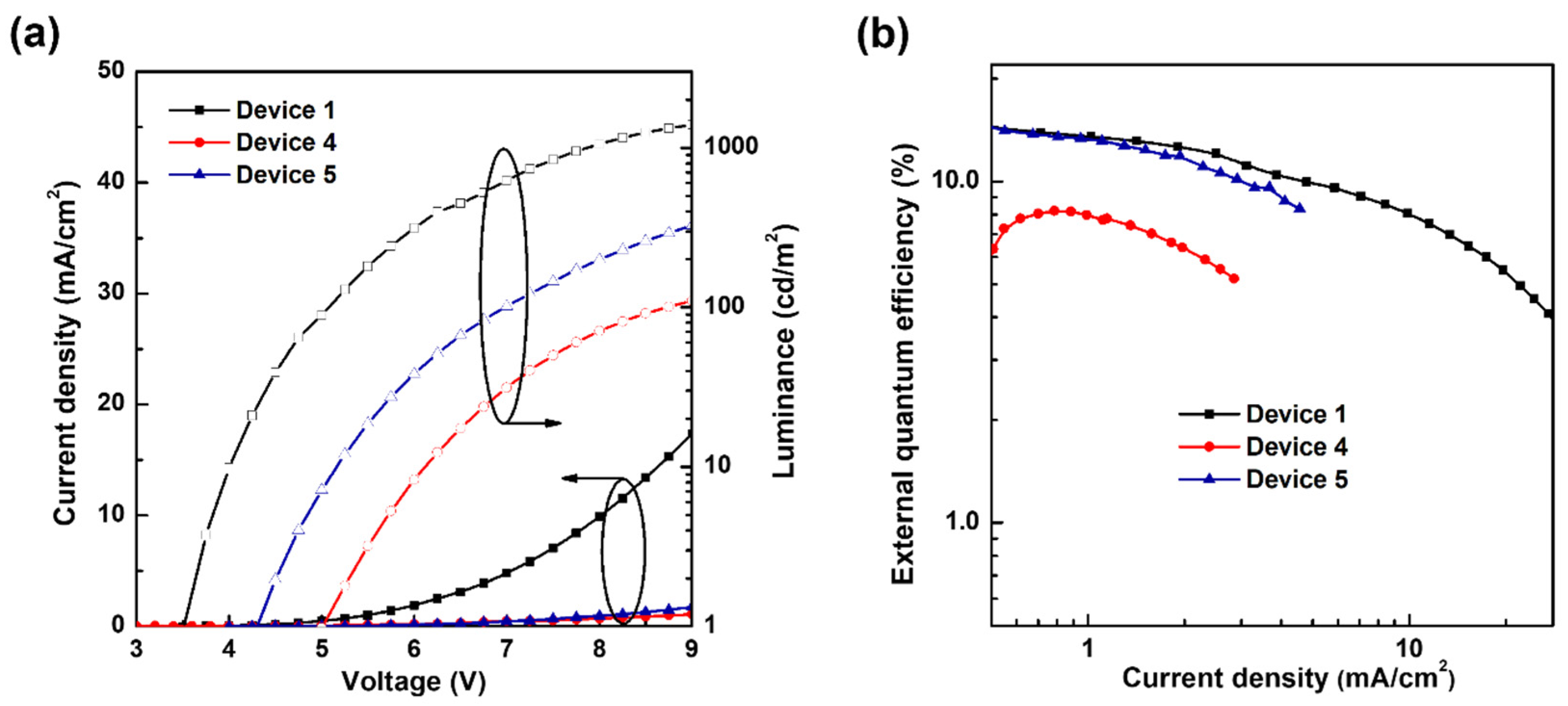
3.2. Analysis of the Degradation of Blue TADF OLEDs by Different ExBL Structures

In this section, the optimization of the blue TADF OLED device with respect to the ExBL thickness is discussed. Due to the high triplet energy of the blue TADF dopant (DMAC-DPS), ExBL is essential for the device [28]. Devices 1, 4, and 5 were fabricated with ExBL thicknesses of 10, 0, and 40 nm, respectively. The J-V-L and J-EQE characteristics of the fabricated devices are shown in Figure 4, and Table 5 summarizes the EL characteristics. The turn-on voltage of device 1 was the lowest, and its maximum EQE was the highest among the devices. Furthermore, device 1 exhibited the highest current density and luminance under the same bias conditions, as shown in Figure 4a. Device 1 exhibited the best performance in terms of efficiency, indicating a well-balanced structure.
Figure 5 and Table 6 present the C-V characteristics of devices 1, 4, and 5 before and after electrical aging at a current density of 10 mA/cm2 for 10 min. As previously indicated, the C-V characteristics were measured using impedance spectroscopy. Each device produced an identical C-V plot trend; as the voltage increased, the capacitance decreased shortly after a slight increase.
Many previous studies have demonstrated that DPEPO is an unstable material [29,30]. To investigate the effect of the poor stability of DPEPO on OLED device stability, device 5 was fabricated with an ExBL thickness of 40 nm. As shown in Figure 5c, the voltage at which the peak capacitance appears shifts from 8.1 to 12.0 V. The peak capacitance decreases from 15.6 to 14.7 nF, shifting more than that of device 1, indicating that device 5 is more degraded. This implies that as the DPEPO thickness increases, the device becomes more unstable. In addition to the unstable characteristics of DPEPO, low carrier mobility is another major cause of the high degradation of the device. DPEPO has a low electron mobility of 7.03 × 10⁻⁸ cm2/V·s, compared to other organic materials. The hole mobility for the selected HTL materials was within the range of 10−5–10−4 cm2/V·s [15,20,24]. Due to the large gap between the electron and hole mobilities, the electrons cannot reach the center of the EML, and carrier recombination occurs at the DPEPO/EML interface. Additionally, a slight increase in capacitance within the range of 3 to 6 V can be seen in Figure 5c. We consider this to be caused by the hole being trapped in the HTL/EML interface owing to the imbalanced injection of the hole and electron [31,32].
Device 4 was fabricated without ExBL to determine whether the poor stability and mobility of DPEPO made the device unstable. As shown in Figure 5b, the voltage at which the peak capacitance appears, increases from 8.3 to 10.4 V. The peak capacitance drops from 21.6 to 21.0 nF. The peak capacitance change of device 4 was the smallest. Owing to the removal of the unstable DPEPO and the resultant decrease in the gap between the electron and hole mobility, the charge balance improved significantly, and the number of trapped carriers decreased. However, the lack of ExBL results in a greater change in the voltage of the peak capacitance than in device 1, because further exciton loss occurs owing to the high triplet energy of the dopant. Poor exciton confinement and exciton loss are the EML-induced inferior EL characteristics, as shown in Figure 4. Furthermore, the increase in capacitance at a low voltage, which is a similar pattern to that of device 5, is also considered to be caused by trapped excitons owing to poor exciton confinement. Therefore, a 10 nm thick DPEPO layer is necessary to improve the performance of the device.

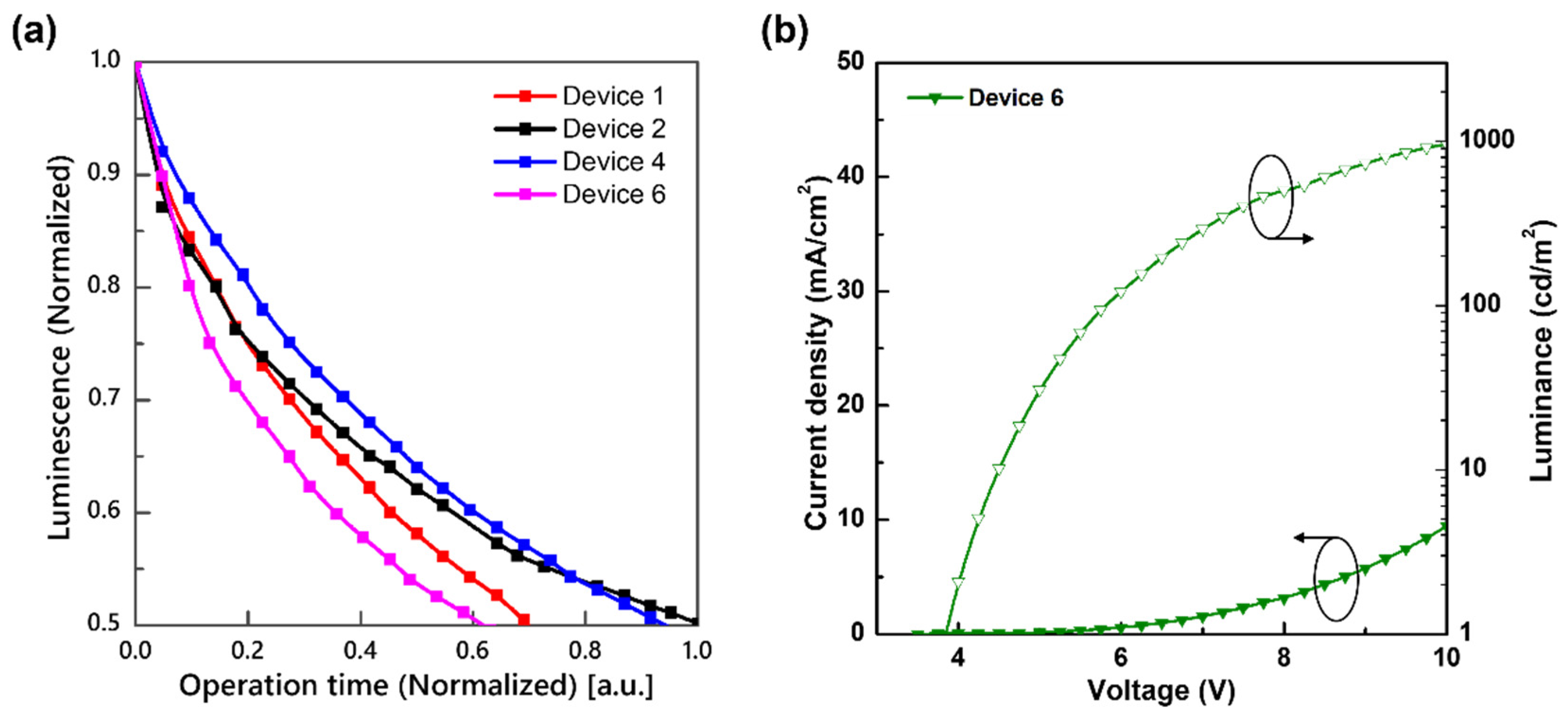
3.3. Operational Stability of Blue TADF OLEDs by Different Structures

Figure 6a shows the normalized luminescence of devices 1, 2, 4, and 6 as a function of operating time when then current density is 10 mA/cm2. Device 6, with an ExBL thickness of 20 nm, was newly fabricated owing to the low luminescence of device 5. The specifications of the structure of device 6 are as follows.
Device 6: NPB 30 nm/TCTA 20 nm/mCP 10 nm/DPEPO: DMAC-DPS 10 wt% 30 nm/DPEPO 20 nm/TPBi 30 nm/LiF 2 nm/Al 80 nm.
Comparing the operational stability of devices 1 and 2, device 2 performed better because of the stable HTL/EML interface characteristic. Note that device 2 showed no significant differences in the peak capacitance value before and after aging (Figure 3b and Table 3); however, the voltage at which the capacitance is the highest shifted more than that for device 1. This confirmed that the operational stability of a device is related more to the peak capacitance drop than to the voltage shift, as previously mentioned.
As previously mentioned in Figure 5 and Table 6, when the ExBL got thicker, the peak capacitance shift ratio increased. Therefore, to determine the effect of ExBL on device stability, we compared the operational stability of devices 1, 4, and 6. The operational stability of device 4 was the best, followed by devices 1 and 6, indicating that the poor stability and low electron mobility of DPEPO made the device unstable.

4. Conclusions

The stability of blue TADF OLEDs was successfully analyzed considering the HTL and ETL structures, and the analysis results were in accordance with the chemical properties of the device material. The C-V characteristics were measured to analyze the degradation features of each fabricated device using a non-destructive and quantitative impedance spectroscopy method. After the device was electrically aged, the peak capacitance value decreased, and the voltage of the peak capacitance increased compared to that of the fresh devices. By comparing the amount of peak capacitance shift, the stability properties were determined at different EML interfaces in terms of the HTL and ETL. For the HTL, the TCTA/EML interface was the most stable of the three types of HTL materials, with a peak capacitance shift ratio of approximately 1.3%. This shift ratio was the smallest in comparison with those of the mCP/EML (3.7%) and NPB/EML (7.4%) interfaces. This could be explained by the higher Tg and BDE of TCTA, which are key indicators of the thermochemical stability of OLED materials. For the ETL, a 10 nm thick ExBL clearly enhanced the EL’s characteristic properties. However, after removing the ExBL, the peak capacitance shift ratio decreased from 3.7% to 2.8%. In addition, for the device containing a 40 nm thick ExBL, the shift ratio increased to 5.8%. Therefore, although the poor stability and low carrier mobility of DPEPO contribute to the high degradation of the device, a 10 nm thick ExBL is necessary to achieve high EL performance. We also successfully demonstrated that investigating the C-V characteristics can analyze the operational stability of the device by measuring the operation time.

Author Contributions

Conceptualization, S.-J.P.; methodology, S.-J.P.; validation, S.-J.P., J.-Y.P., and B.-K.J.; formal analysis, S.-J.P. and J.-Y.P.; investigation, S.-J.P. and J.-Y.P.; resources, S.-J.P. and J.-Y.P.; data curation, S.-J.P. and J.-Y.P.; writing—original draft preparation J.-Y.P.; writing—review and editing, S.-J.P.; visualization, S.-J.P. and J.-Y.P.; supervision, B.-K.J.; project administration, B.-K.J.; funding acquisition, B.-K.J. All authors have read and agreed to the published version of the manuscript.

Funding

This work was supported by Samsung Display Co., Ltd. and the Brain Korea 21 Plus Project in 2022.

Institutional Review Board Statement

Not applicable.

Informed Consent Statement

Not applicable.

Data Availability Statement

Not applicable.

Conflicts of Interest

The authors declare no conflict of interest.

References

  1. Zhang, Q.; Li, B.; Huang, S.; Nomura, H.; Tanaka, H.; Adachi, C. Efficient blue organic light-emitting diodes employing thermally activated delayed fluorescence. Nat. Photonics 2014, 8, 326–332. [Google Scholar] [CrossRef]
  2. Lim, H.; Cheon, H.; Woo, S.; Kwon, S.; Kim, Y.; Kim, J. Highly Efficient Deep-Blue OLEDs using a TADF Emitter with a Narrow Emission Spectrum and High Horizontal Emitting Dipole Ratio. Adv. Mater. 2020, 32, 2004083. [Google Scholar] [CrossRef] [PubMed]
  3. Lee, D.; Choi, J.; Lee, C.; Lee, J. Ideal Molecular Design of Blue Thermally Activated Delayed Fluorescent Emitter for High Efficiency, Small Singlet–Triplet Energy Splitting, Low Efficiency Roll-Off, and Long Lifetime. ACS Appl. Mater. Interfaces 2016, 8, 23190–23196. [Google Scholar] [CrossRef] [PubMed]
  4. Li, X.; Shi, Y.; Wang, K.; Zhang, M.; Zheng, C.; Sun, D.; Dai, G.; Fan, X.; Wang, D.; Liu, W.; et al. Thermally Activated Delayed Fluorescence Carbonyl Derivatives for Organic Light-Emitting Diodes with Extremely Narrow Full Width at Half-Maximum. ACS Appl. Mater. Interfaces 2019, 11, 13472–13480. [Google Scholar] [CrossRef]
  5. Chen, L.; Yu, H.; Dirican, M.; Fang, D.; Tian, Y.; Yan, C.; Xie, J.; Jia, D.; Liu, H.; Wang, J.; et al. Highly Transparent and Colorless Nanocellulose/Polyimide Substrates with Enhanced Thermal and Mechanical Properties for Flexible OLED Displays. Adv. Mater. Interfaces 2020, 7, 2000928. [Google Scholar] [CrossRef]
  6. Nakanotani, H.; Tsuchiya, Y.; Adachi, C. Thermally-activated Delayed Fluorescence for Light-emitting Devices. Chem. Lett. 2021, 50, 938–948. [Google Scholar] [CrossRef]
  7. Uoyama, H.; Goushi, K.; Shizu, K.; Nomura, H.; Adachi, C. Highly efficient organic light-emitting diodes from delayed fluorescence. Nature 2012, 492, 234–238. [Google Scholar] [CrossRef]
  8. Karunathilaka, B.; Balijapalli, U.; Senevirathne, C.; Yoshida, S.; Esaki, Y.; Goushi, K.; Matsushima, T.; Sandanayaka, A.; Adachi, C. Suppression of external quantum efficiency rolloff in organic light emitting diodes by scavenging triplet excitons. Nat. Commun. 2020, 11, 4926. [Google Scholar] [CrossRef]
  9. Nguyen, T.; Nakanotani, H.; Hatakeyama, T.; Adachi, C. The Role of Reverse Intersystem Crossing Using a TADF-Type Acceptor Molecule on the Device Stability of Exciplex-Based Organic Light-Emitting Diodes. Adv. Mater. 2020, 32, 1906614. [Google Scholar] [CrossRef]
  10. Hall, D.; Suresh, S.; dos Santos, P.; Duda, E.; Bagnich, S.; Pershin, A.; Rajamalli, P.; Cordes, D.; Slawin, A.; Beljonne, D.; et al. Improving Processability and Efficiency of Resonant TADF Emitters: A Design Strategy. Adv. Opt. Mater. 2019, 8, 1901627. [Google Scholar] [CrossRef]
  11. Zhang, X.; Fuentes-Hernandez, C.; Zhang, Y.; Cooper, M.; Barlow, S.; Marder, S.; Kippelen, B. High performance blue-emitting organic light-emitting diodes from thermally activated delayed fluorescence: A guest/host ratio study. J. Appl. Phys. 2018, 124, 055501. [Google Scholar] [CrossRef]
  12. Yin, C.; Zhang, D.; Duan, L. A perspective on blue TADF materials based on carbazole-benzonitrile derivatives for efficient and stable OLEDs. Appl. Phys. Lett. 2020, 116, 120503. [Google Scholar] [CrossRef]
  13. Zhang, D.; Cai, M.; Zhang, Y.; Zhang, D.; Duan, L. Sterically shielded blue thermally activated delayed fluorescence emitters with improved efficiency and stability. Mater. Horiz. 2016, 3, 145–151. [Google Scholar] [CrossRef]
  14. Kim, J.; Park, I.; Chan, C.; Tanaka, M.; Tsuchiya, Y.; Nakanotani, H.; Adachi, C. Nanosecond-time-scale delayed fluorescence molecule for deep-blue OLEDs with small efficiency rolloff. Nat. Commun. 2020, 11, 1765. [Google Scholar] [CrossRef] [Green Version]
  15. Kumar, M.; Pereira, L. Effect of the Host on Deep-Blue Organic Light-Emitting Diodes Based on a TADF Emitter for Roll-Off Suppressing. Nanomaterials 2019, 9, 1307. [Google Scholar] [CrossRef] [Green Version]
  16. Jeon, S.; Lee, K.; Kim, J.; Ihn, S.; Chung, Y.; Kim, J.; Lee, H.; Kim, S.; Choi, H.; Lee, J. High-efficiency, long-lifetime deep-blue organic light-emitting diodes. Nat. Photonics 2021, 15, 208–215. [Google Scholar] [CrossRef]
  17. Wang, H.; Xie, L.; Peng, Q.; Meng, L.; Wang, Y.; Yi, Y.; Wang, P. Novel Thermally Activated Delayed Fluorescence Materials-Thioxanthone Derivatives and Their Applications for Highly Efficient OLEDs. Adv. Mater. 2014, 26, 5198–5204. [Google Scholar] [CrossRef]
  18. Peng, X.; Feng, H.; Zhang, J.; Liu, S.; Zhang, L.; Xie, W. Efficient trilayer phosphorescent organic light-emitting devices without electrode modification layer and its working mechanism. Nanoscale Res. Lett. 2018, 13, 310. [Google Scholar] [CrossRef] [Green Version]
  19. Kwak, K.; Cho, K.; Kim, S. Analysis of thermal degradation of organic light-emitting diodes with infrared imaging and impedance spectroscopy. Opt. Express 2013, 21, 29558. [Google Scholar] [CrossRef]
  20. Chen, S.; Jiang, X.; So, F. Hole injection polymer effect on degradation of organic light-emitting diodes. Org. Electron. 2013, 14, 2518–2522. [Google Scholar] [CrossRef]
  21. Cao, L.; Klimes, K.; Ji, Y.; Fleetham, T.; Li, J. Efficient and stable organic light-emitting devices employing phosphorescent molecular aggregates. Nat. Photonics 2020, 15, 230–237. [Google Scholar] [CrossRef]
  22. Baldo, M.; Adachi, C.; Forrest, S. Transient analysis of organic electrophosphorescence. II. Transient analysis of triplet-triplet annihilation. Phys. Rev. B 2000, 62, 10967–10977. [Google Scholar] [CrossRef]
  23. Halls, M.; Yoshidome, D.; Mustard, T.; Goldberg, A.; Kwak, H.; Gavartin, J. Atomic-scale simulation for the analysis, optimization and accelerated development of organic optoelectronic materials. J. Phys. Soc. Jpn. 2015, 54, 561–569. [Google Scholar]
  24. Tsai, M.; Lin, H.; Su, H.; Ke, T.; Wu, C.; Fang, F.; Liao, Y.; Wong, K.; Wu, C. Highly Efficient Organic Blue Electrophosphorescent Devices Based on 3,6-Bis(triphenylsilyl)carbazole as the Host Material. Adv. Mater. 2006, 18, 1216–1220. [Google Scholar] [CrossRef]
  25. Tao, Y.; Yang, C.; Qin, J. Organic host materials for phosphorescent organic light-emitting diodes. Chem. Soc. Rev. 2011, 40, 2943. [Google Scholar] [CrossRef] [PubMed]
  26. Wang, Z.; Li, M.; Gan, L.; Cai, X.; Li, B.; Chen, D.; Su, S. Predicting Operational Stability for Organic Light-Emitting Diodes with Exciplex Cohosts. Adv. Sci. 2019, 6, 1802246. [Google Scholar] [CrossRef] [PubMed]
  27. Ko, S.; Kang, S.; Kim, T. A Silane-Based Bipolar Host with High Triplet Energy for High Efficiency Deep-Blue Phosphorescent OLEDs with Improved Device Lifetime. Chem.–A Eur. J. 2020, 26, 7767–7773. [Google Scholar] [CrossRef]
  28. Zhang, D.; Cai, M.; Bin, Z.; Zhang, Y.; Zhang, D.; Duan, L. Highly efficient blue thermally activated delayed fluorescent OLEDs with record-low driving voltages utilizing high triplet energy hosts with small singlet–triplet splittings. Chem. Sci. 2016, 7, 3355–3363. [Google Scholar] [CrossRef] [Green Version]
  29. Sohn, J.; Ko, D.; Lee, H.; Han, J.; Lee, S.; Lee, C. Degradation mechanism of blue thermally activated delayed fluorescent organic light-emitting diodes under electrical stress. Org. Electron. 2019, 70, 286–291. [Google Scholar] [CrossRef]
  30. Ihn, S.; Lee, N.; Jeon, S.; Sim, M.; Kang, H.; Jung, Y.; Huh, D.; Son, Y.; Lee, S.; Numata, M.; et al. An Alternative Host Material for Long-Lifespan Blue Organic Light-Emitting Diodes Using Thermally Activated Delayed Fluorescence. Adv. Sci. 2017, 4, 1600502. [Google Scholar] [CrossRef]
  31. Mohammed, S.; Taher, M.; Monzir, S.; Sofyan, A. Capacitance-voltage measurements of hetero-layer oleds treated by an electric field and thermal annealing. Int. J. Thin Film Sci. Technol. 2021, 10, 217–226. [Google Scholar]
  32. Zhang, C.; Xu, Z.; Wang, P.; Qin, Z.; Wageh, S.; Al-Ghamdi, A.; Zhao, S. Optical capacitance/conductance-voltage characteristics of stored charges in organic light-emitting diodes. Molecules 2020, 25, 2818. [Google Scholar] [CrossRef] [PubMed]
Figure 1. (a) Energy-diagram and structure of blue TADF OLEDs and (b) chemical structures of organic materials used in the EML.
Applsci 12 13045 g001
Figure 2. (a) J-V-L characteristics and (b) J-EQE characteristics of devices 1, 2, and 3.
Applsci 12 13045 g002
Figure 3. C-V characteristics of blue TADF OLEDs before and after degradation: (a) device 1, (b) device 2, and (c) device 3.
Applsci 12 13045 g003
Figure 4. (a) J-V-L characteristics and (b) J-EQE characteristics of devices 1, 4, and 5.
Applsci 12 13045 g004
Figure 5. C-V characteristics of blue TADF OLEDs before and after degradation: (a) Device 1, (b) Device 4, and (c) Device 5.
Applsci 12 13045 g005
Figure 6. (a) Normalized luminescence of blue TADF OLEDs at J = 10 mA/cm2 as a function of operating time of devices 1, 2, 4, and 6, and (b) J-V-L characteristics of device 6.
Applsci 12 13045 g006
Table 1. Structures of the fabricated blue TADF devices.
DevicesHTLHTLHTLEMLExBLETLEILCathode
30 nm20 nm10 nm30 nmX nm30 nm2 nm80 nm
1NPBTCTAmCPDPEPO: DMAC-DPS (10 wt%)DPEPO (10)TPBiLiFAl
2TCTADPEPO (10)
3DPEPO (10)
4TCTAmCP
5TCTAmCPDPEPO (40)
Table 2. EL characteristics of devices 1, 2, and 3.
Turn-On
Voltage (V)
Maximum External Quantum Efficiency (%)Maximum Power
Efficiency (lm/W)
Device 13.517.717.7
Device 23.97.76.1
Device 34.03.42.6
Table 3. Peak voltage and peak capacitance shift values after degradation of devices 1, 2, and 3.
ΔV 1ΔC 2
Device 10.8 V3.7%
Device 21.1 V1.3%
Device 31.3 V7.4%
1 ΔV: decrement value of the voltage at which the capacitance is maximum. 2 ΔC: reduction ratio of maximum capacitance after degradation.
Table 4. Average BDE, Tg, and ET for selected hole transport materials [24,25,26,27].
Average BDE 1 (eV)Tg (°C)ET (eV)
mCP4.23552.90
TCTA5.241512.76
NPB5.23952.29
1 Average BDE between C-N in cationic state.
Table 5. EL characteristics of devices 1, 4, and 5.
Turn-On
Voltage (V)
Maximum External Quantum Efficiency (%)Maximum Power
Efficiency (lm/W)
Device 13.517.717.7
Device 45.08.24.0
Device 54.214.410.0
Table 6. Peak voltage and peak capacitance shift values after degradation of devices 1, 4, and 5.
ΔV 1ΔC 2
Device 10.8 V3.7%
Device 42.1 V2.8%
Device 53.9 V5.8%
1 ΔV: decrement value of the voltage at which the capacitance is maximum. 2 ΔC: reduction ratio of maximum capacitance after degradation.
Publisher’s Note: MDPI stays neutral with regard to jurisdictional claims in published maps and institutional affiliations.

