Article

A Single-Bit Incremental Second-Order Delta-Sigma Modulator with Coarse-Fine Input Buffer

Department of Electronics Engineering, Chungnam National University, Daejeon 34134, Republic of Korea
*
Author to whom correspondence should be addressed.
Appl. Sci. 2022, 12(22), 11651; https://doi.org/10.3390/app122211651
Submission received: 25 October 2022 / Revised: 12 November 2022 / Accepted: 13 November 2022 / Published: 16 November 2022
(This article belongs to the Section Electrical, Electronics and Communications Engineering)

Abstract

:

Featured Application

Low noise circuit, delta-sigma modulator, analog to digital converter.

Abstract

This paper presents an incremental second-order delta-sigma modulator with a coarse-fine input buffer in 180-nm CMOS. The modulator’s architecture was implemented as a second-order cascade of integrators with a feedback structure. The switched-capacitor integrator was operated in discrete time, with high-gain amplifiers required to achieve improved performance during the integration phase. The amplifier comprised rail-to-rail input and gain-boosted cascode intermediate stages, thus achieving a high gain and wide input voltage range. The circuit adopts a coarse-fine buffer for higher performance. The coarse buffer is operated first to enable fast settling through a high slew rate, followed by the fine buffer to satisfy the low-noise and high-accuracy characteristics. The fine buffer has a smaller current consumption with higher power efficiency. The experiment results show that the proposed input buffer achieved a 13.14 effective number of bits and an 80.87 dB signal-to-noise and distortion ratio. The modulator operates a single bit and sampling clock at 125 kHz. The proposed delta-sigma modulator was operated at 1.8 V. The proposed circuit was designed using a standard 0.18-μm CMOS process with an active area of 1.06 mm2. The total current consumption with the coarse-fine buffer was 1.374 mA.

1. Introduction

Analog-to-digital converters (ADCs) have attracted considerable attention for their potential in applications that require high resolution, such as wearable bio-signal sensors [1] or biosensor arrays [2,3]. Delta-sigma modulation (DSM) ADCs are often chosen for processing low-frequency signals, which are within a few kilohertz [4]. Many high-precision sensors were reported with high-resolution DSM, such as the Hall sensor [5], electrochemical sensor [6], bridge sensor [7], and so on. Among the various DSM architectures, the incremental DSM [8,9] is widely used for multiplexing between multichannel inputs [10,11,12]. To achieve high resolution, the DSMs with second or higher-order noise shaping have been employed for achieving high-resolution [13,14]. The delta-sigma input stage is designed for continuous time (CT) or discrete time (DT) [15]. Oversampling and noise shaping are widely used to realize low-noise characteristics, so the input stage of the DSM acts as the high-frequency switching load at the point of the input buffer view. Assuming tens to thousands of oversampling rates (OSRs), the input buffer inside the DSM should operate as fast as the OSR times the output rate of the DSM. Fast operations cause higher power consumption, making the implementation of the buffer design a challenge in high-resolution ADC design. Moreover, when converting an analog input signal, the input signal is often corrupted by kickback noise [16] from the conversion. To prevent signal degradation, an input buffer with precise settling characteristics within the desired sampling period is highly desired.
Figure 1 shows the conventional and proposed input buffer schemes. In the conventional input buffer scheme, the input buffer drives the input-switching loads of the DSM input stage. A buffer is required to drive the input stage, and a high slew rate, power, and speed are required to achieve high-resolution performance. High power is required to drive the CT and DT input stages using a single buffer. As shown in Figure 1a, a pre-charge scheme has been reported to relax buffer requirements [17,18]. The internal pre-charge buffer relaxes the external buffer specifications [19,20]. Fast charging has been performed with the assistance of a pre-charge buffer [17,18,19,20]; the external buffer settled only a small voltage to the final desired value. In [21], the low noise fully differential amplifier (THP210, Texas Instruments, Dallas, TX, USA) drives the DSM (ADS127L11, Texas Instruments, Dallas, TX, USA), which includes the pre-charge buffer, and the current consumption of the driving amplifier is 950 uA. In this paper, a single-bit incremental second-order DSM with a coarse-fine input buffer is proposed.
The proposed input buffer with a parallel coarse fine buffer scheme is shown in Figure 1b. In existing technologies, DSM performance is limited by the driving ability of the external fine buffer. In the proposed scheme, the coarse-fine input buffer is integrated; thus, no external buffer is required. The coarse-fine input buffer includes two buffers: a pre-charge buffer and a fine settling buffer. Using the coarse-fine input buffer, both the fast settling and low noise characteristics can be achieved. Considering the circuit area and power consumption of the external buffer in the conventional scheme, the area and power consumption penalty of the proposed coarse-fine buffer is negligible. In our proposed DSM ADC, the input buffer and secondary DT DSM are integrated.
The operational concept of the coarse-fine buffer-based input buffer circuit is shown in Figure 2. In this paper, the pre-charge and fine paths were placed in parallel; coarse pre-charge was performed by the pre-charge path buffer according to the timing, and then fine settling was performed by the low-noise fine buffer. A fast buffer that drives the coarse path and a low-noise fine path buffer were built in parallel, and the internal voltage was precisely settled with the fine buffer after charging most of the voltage with the coarse buffer. The proposed scheme integrates the buffer and DSM to achieve stable performance without an external buffer. The circuit designed in this research can be applied to precise measurement requiring low-noise analog signal processing without a separate external buffer.

2. Proposed Delta Sigma Modulator with Coarse-Fine Input Buffer

The block diagram of the proposed circuit is shown in Figure 3. The circuit comprises two main parts: a coarse-fine, pre-charged buffer that acquires analog signals and a DSM that post-processes it. Both circuits require timing circuits to optimize their performance. The operational times of the coarse and fine buffers are partially shared. The input buffer internal chopper clock uses a frequency of 16 kHz. The unintended noise in the low-frequency band can be significantly reduced through chopper modulation. The sampling signal used was 125 kHz, higher than the chopper frequency, and the oversampling rate was set at 512. The circuit characteristics can be controlled by externally adjusting the resistor through a serial peripheral interface (SPI). Through SPI logic manipulation, modulator and buffer blocks can be enabled or disabled, and the performance of each block is tested.

2.1. Coarse-Fine Input Buffer

A coarse-fine input buffer was used for fast, low-noise, characteristic-based analog signal acquisition. As shown in Figure 4, the input buffer comprises a parallel connection between the coarse and fine buffers and a timing circuit. The main characteristics of coarse circuits are that they are faster and noisier than fine buffers. To compensate for this, a low-noise but slow fine buffer was connected in parallel. The acquisition of analog signals with high speed and low noise can be achieved through two complementary and timing circuits. The circuit had two inputs and two outputs; the output was fed to a DSM for the post-processing of the acquired analog signal. For low-noise characteristics, a fine buffer must have high voltage gain characteristics.
The chopper technique was used to reduce flicker noise in the low-frequency band [22,23] in the fine buffer. The input chopper modulates the input signal to a higher frequency and prevents degradation due to the low-frequency noise. The output chopper demodulates the input signal to the baseband and also modulates the low-frequency noise of the amplifier to the high-frequency band; thus, a high signal-to-noise ratio can be achieved.
The coarse buffer was designed to operate with the unit-gain bandwidth of 3 MHz. The bandwidth of the fine buffer is limited by the chopper frequency. The chopper is operated at 16 kHz. The output stage of the fine and coarse buffers is designed using the Monticelli-style class-AB amplifier circuit [24] to enhance the driving capability of the switching load.
The amplifier used for the coarse buffer is shown in Figure 5. The circuit was a single-ended Monticelli amplifier circuit. A rail-to-rail input output-type circuit was used for a wide range of analog signal inputs and outputs. A Miller compensation capacitor is used from the class-AB output terminal for the stable operation of the circuit.
The amplifier used in the fine buffer is shown in Figure 6. The circuit structure is similar to that of the coarse buffer circuit. However, a chopper is used between the input and output stages to focus on the low-noise characteristics. In the input stage, the signal was modulated using a chopper, and the folded cascode stage was demodulated. There is a difference in the total amount of current compared to the coarse buffer. Low-noise characteristics can be achieved by adjusting the input differential amplifier stage and the folded-cascode stage current ratio. To optimize the gm value, which is important for optimizing low-noise characteristics, a fine buffer can achieve low-noise characteristics. Coarse and fine buffers have similar circuit structures but complementary characteristics. The coarse buffer is responsible for operating characteristics over a wide frequency range, while the fine buffer has high voltage gain and low noise characteristics. Figure 7 shows the transient simulation results for the optimal timing of each buffer. The enable time of the coarse buffer is slightly shorter than that of the fine buffer. Two buffer enable times of approximately 1 μs were shared. Both enable the signals to operate at a frequency of 125 kHz. The signal is stabilized by the fine buffer after the pre-charge of the coarse buffer with a fast settling time.

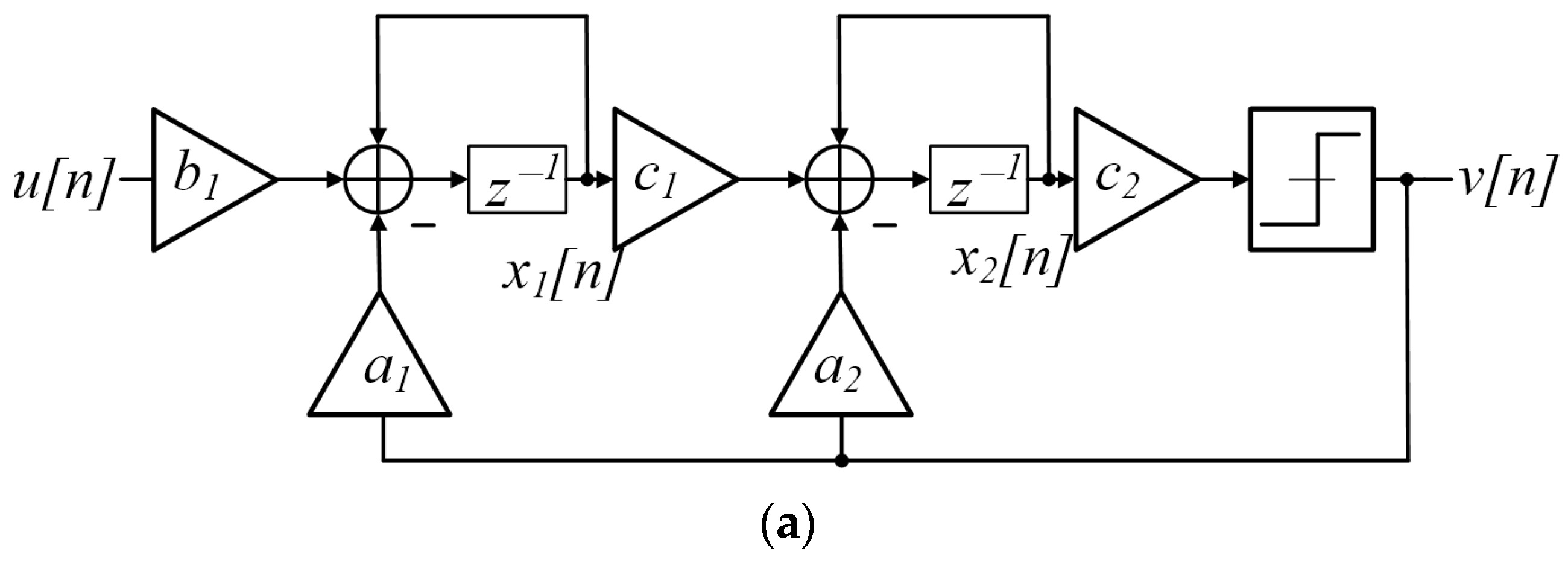
2.2. Second-Order Incremental Cascade of Integrator Feedback

The DSM circuit is designed as a second-order cascade of an integrator with feedback (CIFB). Figure 8a shows the block diagram of the secondary CIFB circuit. Figure 8b shows the schematic of the modulator. The OSR in the secondary modulator circuit is assumed to be 512. Moreover, the sampling frequency was set to 125 kHz, and the passband frequency was given to 122.07 Hz. From the assumed parameters, the noise transfer function (NTF) and signal transfer function (STF) are expressed as follows:
N T F = ( z 1 ) 2 ( z 2 1.225 z + 0.4415 )
S T F = 0.21637 ( z 2 1.225 z + 0.4415 )
The coefficients a1, a2, b1, and c1 are designed to satisfy the following relationship (3) when the supply voltage of the circuit (Vdd) was at 1.8 V:
a 1 = C 1 V d d C 2 ,   a 2 = C 4 V d d C 5 ,   b 1 = C 1 V d d C 2 ,   c 1 = C 3 C 5
The coefficients are calculated using the MATLAB behavioral model and approximated according to the design rule of the metal-insulator-metal (MIM) capacitors. The coefficients are summarized in Table 1.
The amplifier used in the DSM integrator is shown in Figure 9. The circuit was designed as a fully differential amplifier (FDA) with rail-to-rail input and output to maximize the voltage input and output. A Miller compensation capacitor was used to stabilize the frequency band of the circuit. A gain-boosting technique was used to optimize the voltage gain. In the folded cascode amplification circuit, electrical signals are input from the sources of MP6 and MP7, and of MN6 and MN7. The amplified electrical signal is then outputted to the gates. MP12, MP13, MP14, MP15, MN13, and MN14 were used as common-mode feedback circuits.
Figure 10 shows the loop gain simulation of the FDA used as an integrator. The DC gain, unit gain bandwidth, and phase margin are 180 dB, 1.8 MHz, and 60°, respectively. The FDA draws approximately 210 μA at a voltage supply of 1.8 V.
The PMOS and NMOS gain-boosting circuits are shown in Figure 11a,b, respectively. These circuits are used for Gmn and Gmp in Figure 9. The Gmn and Gmp are designed using a folded-cascode amplifier configuration. The Gmn and Gmp provide the boosted gain of Equations (4) and (5), respectively.
Gmn = gmn1(ron1||rop1)(gmp3rop3)||(gmn8ron8ron4)
Gmp = gmp2(rop2||ron1)(gmn3ron3)||(gmp6rop6rop4)
The two-stage comparator at the end of the modulator stage is shown in Figure 12. The pre-amplifier stage is designed using the PMOS input stage and the gain-enhanced positive feedback NMOS loads (MN2 and MN3) and diode-connected loads (MN1 and MN4). The second stage is designed using the dynamic latch and the following SR-latch.

3. Results and Discussion

A chip die photograph of the circuit is shown in Figure 13. The circuit was fabricated using the TSMC 180 nm process. The supply voltage operates at 1.8 V, and the supply current is 1.4 mA. The active area of the circuit is 1.06 mm2.
Figure 14 shows the output transient measurement results for the buffer according to the sinusoidal input. The activation timings of the coarse buffer and fine buffer are shown in Figure 15. The coarse-fine buffer can drive the input switching load of the DSM.
To measure the slew rate of the input buffer, the step input with the magnitude of 200 mV, from 800 mV to 1 V, is applied. The slew rate was 2.13 V/μs for the voltage arrival times from 10% to 90% of signal amplitude.
Figure 16 shows the input-referred noise measurement results for the coarse and fine buffers. To measure the buffer noise, the output of the buffer was amplified using the low-noise voltage amplifier SR560 (Stanford Research Systems, Sunnyvale, CA, USA). The input-referred noise floor of the coarse buffer was measured to be 36 nV/rtHz 100 Hz, and that of the fine buffer was measured to be 17 nV/rtHz. The coarse and fine buffers used currents of approximately 225 and 270 μA, respectively. As shown in Figure 16 and Figure 17, it is possible to achieve a fast settling time and low noise characteristics simultaneously through coarse and fine buffers.
Figure 18 shows the sampling clock and bitstream output results as functions of the sinusoidal input. The frequency of the input sine wave was applied at 100 Hz, 1.2 Vpp, and 900 mV common mode voltage. The sampling clock was set to 125 kHz, and the OSR was set to 512 during the design process. It was observed that the bitstream output changed according to high and low sine waves. The result of the pulse density modulation (PDM) FFT analysis based on the bitstream output result is shown in Figure 19. Analysis of the PDM signal was performed using an APX500 (Audio Precision, 5750 SW Arctic Dr, Beaverton, OR 97005, NA). The passband frequency was determined from the Nyquist frequency of the sampling frequency and oversampling rate, which was 122.07 Hz. Performance indicators such as ENOB, SINAD, and the spurious free dynamic range of the modulator were calculated based on the above, with the average noise floor at −113 dB. Based on this, we calculated the RMS value of the noise up to the passband, wherein the signal’s amplitude was −10 dB. The calculated SINAD and ENOB were 80.87 dB and 13.14 bits, respectively.

4. Conclusions

A summary of the performance achievements of this research is shown in Table 2. In the DSM operated with high OSRs, high-speed input buffers are required to drive the input stage of the DSM. The overall performances of the DSMs are highly dependent on the characteristics of the input buffers. The pre-charge scheme can relax the requirement of the input buffers. However, still low noise input buffers are required. Moreover, it is hard to optimize the power consumption and performance of the system using the commercial-off-the-shelf (COTS) components. In this paper, a single-bit incremental second-order DSM with a fully integrated coarse-fine input buffer without an external buffer was presented. In the coarse-fine input buffer, two parallel buffers, the pre-charge buffer and fine-settling buffer, are included. Using the coarse-fine input buffer, both the fast settling and low noise characteristics can be achieved. The proposed input buffer achieved an ENOB and SINAD of 13.14 and 80.87 dB, respectively. The modulator operates a single bit and sampling clock at 125 kHz. The proposed DSM was operated at 1.8 V. The proposed circuit was designed using a standard 0.18-μm CMOS process with an active area of 1.06 mm2. The total current consumption with the coarse-fine buffer was 1.374 mA.

Author Contributions

Conceptualization and supervision, H.K.; circuit design, measurement, and draft preparation, M.Y.; investigation, K.N.; visualization, G.C.; methodology, S.K.; writing—review and editing, B.J.; format analysis, H.S.; conceptualization, K.K.; project administration, H.K.; funding acquisition, H.K. All authors have read and agreed to the published version of the manuscript.

Funding

This work was funded by the Ministry of Health and Welfare (MOHW, Korea) and the Korea Health Industry Development Institute (KHIDI, Korea). This work was supported by the Practical Technology Development Medical Microrobot Program (R&D Center for Practical Medical Microrobot Platform, HI19C0642); the Ministry of Science and ICT (MSIT), Korea, under the Information Technology Research Center (ITRC) support program (IITP-2021-2017-0-01635) supervised by the Institute for Information & Communications Technology Planning and Evaluation (IITP), and the Nanomedical Devices Development Project of NNFC.

Institutional Review Board Statement

Not applicable.

Informed Consent Statement

Not applicable.

Data Availability Statement

Not applicable.

Acknowledgments

The EDA tool was supported by the IC Design Education Center (IDEC) in Korea.

Conflicts of Interest

The authors declare no conflict of interest.

References

  1. Van Helleputte, N.; Konijnenburg, M.; Pettine, J.; Jee, D.-W.; Kim, H.; Morgado, A.; Van Wegberg, R.; Torfs, T.; Mohan, R.; Breeschoten, A.; et al. A 345 μW multi-sensor biomedical SoC with bio-impedance, 3-channel ECG, motion artifact reduction, and integrated DSP. IEEE J. Solid-State Circuits 2015, 50, 230–244. [Google Scholar] [CrossRef]
  2. Chen, C.-H.; Zhang, Y.; He, T.; Chiang, P.Y.; Temes, G.C. A micro-power two-step incremental analog-to-digital converter. IEEE J. Solid-State Circuits 2015, 50, 1796–1808. [Google Scholar] [CrossRef]
  3. Agah, A.; Vleugels, K.; Griffin, P.B.; Ronaghi, M.; Plummer, J.D.; Wooley, B.A. A high-resolution low-power oversampling ADC with extended-range for bio-sensor arrays. IEEE Symp. VLSI Circuits 2007, 2007, 244–245. [Google Scholar]
  4. Chen, C.H.; Crop, J.; Chae, J.; Chiang, P.; Temes, G.C. ‘A 12- bit 7 μW/channel 1 kHz/channel incremental ADC for biosensor interface circuits. In Proceedings of the 2012 IEEE International Symposium on Circuits and Systems (ISCAS), Seoul, Republic of Korea, 20–23 May 2012; pp. 2969–2972. [Google Scholar]
  5. Lee, J.Y.; Oh, Y.; Oh, S.; Chae, H. Low power CMOS-based Hall sensor with simple structure using double-sampling delta-sigma ADC. Sensors 2020, 20, 5285. [Google Scholar] [CrossRef]
  6. Sutula, S.; Cuxart, J.P.; Gonzalo-Ruiz, J.; Munoz, P.; Terés, L.; Serra-Graells, F. A 25-µW All-MOS Potentiostatic Delta-Sigma ADC for Smart Electrochemical Sensors. IEEE Trans. Circuits Syst. I Regul. Pap. 2014, 61, 671–679. [Google Scholar] [CrossRef]
  7. Wu, R.; Chae, Y.; Huijsing, J.H.; Makinwa, K.A. A 20-b ± 40-mV Range Read-Out IC with 50-nV Offset and 0.04% Gain Error for Bridge Transducers. IEEE J. Solid-State Circuits 2012, 47, 2152–2163. [Google Scholar] [CrossRef]
  8. Caldwell, T.C.; Johns, D.A. Incremental data converters at low oversampling ratios. IEEE Trans. Circuits Syst. I 2010, 57, 1525–1537. [Google Scholar] [CrossRef] [Green Version]
  9. Markus, J.; Silva, J.; Temes, G.C. Theory and applications of incremental delta-sigma converters. IEEE Trans. Circuits Syst. I 2004, 51, 678–690. [Google Scholar] [CrossRef] [Green Version]
  10. Oike, Y.; El Gamal, A. CMOS image sensor with per-column ΣΔ ADC and programmable compressed sensing. IEEE J. Solid-State Circuits 2013, 48, 318–328. [Google Scholar] [CrossRef]
  11. Kavusi, S.; Kakavand, H.; Gamal, A.E. On incremental ΣΔ modulation with optimal filtering. IEEE Trans. Circuits Syst. I Reg. Pap. 2006, 53, 1004–1015. [Google Scholar] [CrossRef] [Green Version]
  12. Kim, J.-H.; Jung, W.-K.; Lim, S.-H.; Park, Y.-J.; Choi, W.-H.; Kim, Y.-J.; Kang, C.-E.; Shin, J.-H.; Choo, K.-J.; Lee, W.-B.; et al. A 14b extended counting ADC implemented in a 24Mpixel APS-C CMOS image sensor. In Proceedings of the 2012 IEEE International Solid-State Circuits Conference, San Francisco, CA, USA, 19–23 February 2012; pp. 390–392. [Google Scholar]
  13. Chen, C.-H.; He, T.; Zhang, Y.; Temes, G.C. Incremental analog-to-digital convertors for high-resolution energy-efficient sensor interfaces. IEEE J. Emerg. Sel. Top. Circuits Syst. 2015, 5, 612–623. [Google Scholar] [CrossRef]
  14. Robert, J.; Deval, P. A second-order high-resolution incremental A/D converter with offset and charge injection compensation. IEEE J. Solid-State Circuits 1988, 23, 736–741. [Google Scholar] [CrossRef]
  15. Keith, N.; EDN Asia. Understanding the Benefits of pre-Charge Buffers in ADCs. 2021. Available online: https://www.ednasia.com/understanding-the-benefits-of-pre-charge-buffers-in-adcs (accessed on 19 October 2022).
  16. Razavi, B. The delta-sigma modulator [A circuit for all seasons]. IEEE Solid-State Circuits Mag. 2016, 8, 10–15. [Google Scholar] [CrossRef]
  17. ADS127L11 400-KSPS, Wide-Bandwidth, 24-Bit, Delta-Sigma ADC Datasheet. Available online: https://www.ti.com/lit/ds/symlink/ads127l11.pdf (accessed on 17 October 2022).
  18. Gupta, S.; Rathi, S.J.; Balamurali, S. Pre-Charge Buffer for Analog-to-Digital Converter. U.S. Patent 9571118B1, 14 February 2017. [Google Scholar]
  19. Castilho, M.A.L. Design of a Reference Buffer for a Delta-Sigma ADC with Current DAC. Master’s Thesis, Universidade Nova de Lisboa, Lisbon, Portugal, 2019. [Google Scholar]
  20. Dirk, K. Sigma-Delta Modulator. U.S. Patent EP1837996B1, 20 October 2010. [Google Scholar]
  21. THP210 and ADS127L11 Performance Table of Contents Application Note. Available online: https://www.ti.com/lit/an/sboa546/sboa546.pdf (accessed on 17 October 2022).
  22. Enz, C.C.; Temes, G.C. Circuit techniques for reducing the effects of op-amp imperfections: Autozeroing, correlated double sampling, and chopper stabilization. Proc. IEEE 1996, 84, 1584–1614. [Google Scholar] [CrossRef] [Green Version]
  23. Lee, C.-J.; Song, J.-I. A chopper stabilized current-feedback instrumentation amplifier for EEG acquisition applications. IEEE Access 2019, 7, 11565–11569. [Google Scholar] [CrossRef]
  24. Hogervorst, R.; Tero, J.P.; Eschauzier, R.G.H.; Huijsing, J.H. A compact power-efficient 3 v CMOS rail-to-rail input/output operational amplifier for VLSI cell libraries. IEEE J. Solid-State Circuits 1994, 29, 1505–1513. [Google Scholar] [CrossRef] [Green Version]
  25. Kumar, R.S.A. A Discrete-Time Delta-Sigma Modulator with Relaxed Driving Requirements And Improved Anti-Aliasing. In Proceedings of the 2021 IEEE International Symposium on Circuits and Systems (ISCAS), Daegu, Republic of Korea, 22–28 May 2021; pp. 1–5. [Google Scholar]
  26. Wang, T.; Xie, T.; Liu, Z.; Li, S. An 84dB-SNDR Low-OSR 4th-Order Noise-Shaping SAR with an FIA-Assisted EF-CRFF Structure and Noise-Mitigated Push-Pull Buffer-in-Loop Technique. In Proceedings of the 2022 IEEE International Solid-State Circuits Conference (ISSCC), San Francisco, CA, USA, 20–26 February 2022; pp. 418–420. [Google Scholar]
  27. Wei, R.; Wang, J.; Su, H. A fast-response reference voltage buffer for a sigma-delta modulator. IEICE Electron. Expr. 2018, 15, 20180159. [Google Scholar] [CrossRef]
  28. Nikas, A.; Jambunathan, S.; Klein, L.; Voelker, M.; Ortmanns, M. A low distortion continuous time sigma delta modulator using a high input impedance instrumentation amplifier for neural recording. In Proceedings of the 2018 IEEE Biomedical Circuits and Systems Conference (BioCAS), Cleveland, OH, USA, 17–19 October 2018; pp. 1–4. [Google Scholar]
Figure 1. Conventional and proposed input buffer scheme: (a) Conventional external input buffer with internal pre-charge buffer; (b) Proposed internal coarse-fine dual input buffer.
Applsci 12 11651 g001
Figure 2. Working process of coarse-fine input buffer.
Applsci 12 11651 g002
Figure 3. Block diagram of the proposed circuit.
Applsci 12 11651 g003
Figure 4. Schematic of coarse-fine input buffer.
Applsci 12 11651 g004
Figure 5. Schematic of the coarse input buffer.
Applsci 12 11651 g005
Figure 6. Schematic of the fine input buffer.
Applsci 12 11651 g006
Figure 7. Transient simulation result of the buffer’s enable timing diagram.
Applsci 12 11651 g007
Figure 8. (a) Block diagram; (b) Schematic of second-order delta-sigma modulator.
Applsci 12 11651 g008aApplsci 12 11651 g008b
Figure 9. Fully differential amplifier for integrator.
Applsci 12 11651 g009
Figure 10. FDA loop gain simulation result in integrator.
Applsci 12 11651 g010
Figure 11. Gain boosting amplifier of Gmp (a) and Gmn (b).
Applsci 12 11651 g011
Figure 12. Schematic of the two-stage comparator.
Applsci 12 11651 g012
Figure 13. Die photograph of the proposed circuit.
Applsci 12 11651 g013
Figure 14. Transient measurement result of coarse-fine input buffer.
Applsci 12 11651 g014
Figure 15. Enable timing signal measurement of coarse and fine buffers.
Applsci 12 11651 g015
Figure 16. Noise measurement result of coarse and fine buffers.
Applsci 12 11651 g016
Figure 17. Transient measurement results of square input signal and output signal of buffer.
Applsci 12 11651 g017
Figure 18. Sinusoidal signal of buffer output and bitstream output.
Applsci 12 11651 g018
Figure 19. Sinusoidal input signal and bitstream output.
Applsci 12 11651 g019
Table 1. Comparison of simulated ideal coefficients and actual coefficients designed with MIM capacitors.
CoefficientIdeal ValueReal Value
a10.11250.1112
a20.180.1776
b10.11250.1112
c10.450.4365
Table 2. Performance summary comparison between the proposed delta-sigma modulator with previous studies.
This WorkISCAS 2021
[25]
ISSCC 2022
[26]
IEICE 2018
[27]
BIOCAS 2018
[28]
Process(μm)0.180.180.0650.180.18
Supply voltage (V)1.81.81.21.81.8
Current consumption (A)1.374 m480 μ61.9 μ 81.5 μ14 μ
Oversampling rate5121285-256
Order of modulator2nd4th4th --
DT/CTDTDTCTDTCT
SINAD (dB)80.8797.784.164.680
ENOB (bits)13.1415.9713.6710.3413
Sampling frequency (Hz)125 k6.144 M5 M10 k1 M
Pass band frequency (Hz)122.0724 k500 k-4 k
Buffer usage (Y/N)YYYYN
Settling time (s)130 n--134 n-
Publisher’s Note: MDPI stays neutral with regard to jurisdictional claims in published maps and institutional affiliations.

