Article

Research on the Processing of Microstructures on Silicon Carbide Surfaces Using a Blowing-Assisted Nanosecond Laser

School of Mechanical Engineering, Jiangsu University of Technology, Changzhou 213001, China
*
Author to whom correspondence should be addressed.
Appl. Sci. 2022, 12(21), 11234; https://doi.org/10.3390/app122111234
Submission received: 5 October 2022 / Revised: 29 October 2022 / Accepted: 2 November 2022 / Published: 5 November 2022

Abstract

:
The properties of high strength, wear resistance, and high brittleness, make silicon carbide (SiC) materials difficult to process by traditional processing methods. The non-traditional processing method of laser processing has emerged as a viable means of processing silicon carbide materials, as it is very suitable for processing hard and brittle materials, and has the additional advantages of no tool wear, no cutting force, and high processing efficiency. However, in conventional laser processing of silicon carbide, oxidation products occur in the processing area, which can hinder the further removal of the material. To avoid the accumulation of oxidation products and improve the laser processing of the groove structure on the silicon carbide surface, a blowing-assisted laser processing method is proposed by this paper. Comparison experiments between conventional and blowing-assisted laser processing were conducted, in which groove structures of different depths and widths were processed. Two models were established based on the experimental results to explain the material removal process. Finally, the array microgroove structures were successfully processed by blowing-assisted laser processing, verifying the feasibility of improving the laser processing capability of microstructures on silicon carbide surfaces with the assistance of blowing.

1. Introduction

Silicon carbide (SiC) is a strong, covalent bond compound with high strength, high wear resistance, an excellent low coefficient of thermal expansion and corrosion resistance, and is often used for high-precision structural components, such as bearings, rotors, space telescopes [1,2,3]. In addition, due to its large band gap width, strong radiation resistance, and high breakdown field strength, silicon carbide is also used in the production of optical and electronic devices [4,5]. However, owing to its high hardness and brittleness, silicon carbide is a difficult material to machine into the desired structural components with high surface quality and dimensional accuracy by conventional processing method, especially for the processing of microstructures [6,7,8].
Laser processing is a non-traditional processing method that uses high energy lasers to melt or vaporize material to produce components. Compared with traditional processing, laser processing is very suitable for processing hard and brittle materials, and has the additional advantages of no tool wear, no cutting force and high processing efficiency. Microstructures, such as microholes and microgrooves, have been successfully processed on silicon carbide using laser processing [9,10,11].
In the laser processing of silicon carbide, the temperature of the workpiece surface rises rapidly after absorbing laser energy, and silicon carbide is melted and sublimated under high temperature [12,13,14]. The ablation mechanism of silicon carbide in laser processing has been studied by many scholars. Pecholt et al. processed the 3C-SiC material using a femtosecond pulsed laser, and their results showed that the ablation mechanisms were correlated with pulse energy, higher pulse energy generated significant amounts of recast oxide layers and damaged fragments, and the leading material removal mechanisms were photomechanical fragmentation, ultrafast melting, and vaporization with appropriate energy density [15]. Dong et al. investigated the femtosecond pulsed laser micro-processing of the 4H-SiC material, and they proposed several material removal mechanisms for 4H-SiC in femtosecond laser ablation, which included normal melting, thermal vaporization, phase explosion, and photomechanical fragmentation [16]. Zhai et al. studied the thermal ablation behavior of C/SiC material processed by a high repetition frequency femtosecond laser, and found that material oxidation was an obvious defect caused by the thermal effect of the laser that seriously affected the processing quality of microstructures [17]. Hao et al. reported that melting, sublimation, and solidification was observed in the nanosecond laser processing of C/SiC material, and serious defects, such as recast oxidation, debris, and residuals, were formed at the edge of processing area, and the ablation surface quality could be improved by optimizing the parameters [18]. The above research shows that the generation of oxidation products in the laser processing of silicon carbide cannot be ignored, as it has a negative effect on the processing quality of microstructures on silicon carbide surfaces.
Many methods have been trialed that could improve the feasibility of laser processing microstructures on silicon carbide. Cheong et al. processed silicon carbide material in water by laser processing, and they found that the oxide products were not formed, and that microstructures with good quality were processed by controlling the laser parameters and water flow velocity [19]. Iwatani et al. drilled silicon carbide by laser in water, and found that the auxiliary of water could reduce defects on hole surfaces, such as debris, cracks, and heat affected zones, but the processing efficiency was reduced due to the laser energy loss in water [20]. Khuat et al. used a combination of laser and acid etching to machine through holes on silicon carbide material, and they found that the acid etching could effectively remove laser affected zones and improve the processing quality [21]. However, there are still many challenges for the above methods to overcome before they can be effectively used in industrial applications [22,23].
This paper introduces a blowing-assisted laser processing method to improve the laser processing capability of microstructures on silicon carbide surface. Comparison experiments between conventional and blowing-assisted laser processing were conducted, in which groove structures of different depths and widths were processed. The surface quality of the processed area was observed by optical tool microscopy and scanning electron microscopy (SEM), and the composition of different areas of the processed surface was analyzed by energy spectroscopy (EDS). The results showed that the oxidation products were reduced at the edge and center of the grooves due to the blowing, and the processing quality of the groove was also significantly improved. Thus, this study is a good reference point for the laser processing of silicon carbide and its composites in engineering applications.

2. Experimental Procedure

2.1. Material

The material used in the experiments were made by pressureless sintering at 2373–2473 K, and the purity of silicon carbide was 98.5%. The other specific performance parameters are shown in Table 1.

2.2. Description of Blowing-Assisted Laser Processing

Blowing-assisted laser processing was proposed based on conventional laser processing. As shown in Figure 1, a high-speed galvanometer laser marking machine (MDK-GX-20Z, Suzhou, China) was used for laser processing. The laser device was a fiber laser with a wavelength of 1064 nm, pulse width of 100 ns, and the beam spot size was 0.05 mm. The workpiece was placed on the precision X-Y platform to ensure the processing area was in the center of the galvanometer in each experiment. An air pump with an output pressure of 0.6 MPa was used for auxiliary blowing, the air nozzle size was 3 mm × 6 mm, and it blew air directly into the processing area.

2.3. Experimental Design

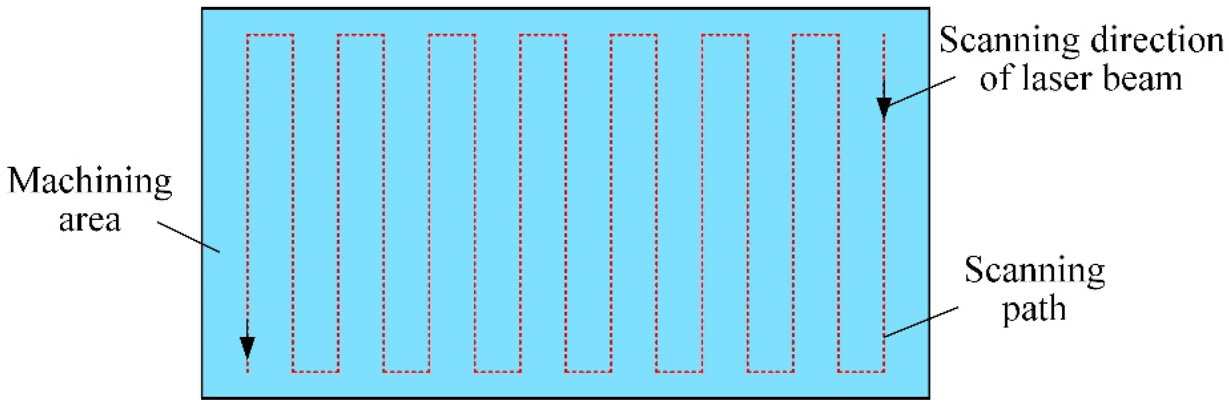
Firstly, the silicon carbide workpiece was processed a different number of speeds by conventional laser processing to obtain the laser processing characteristics of silicon carbide. The same experiments were repeated with blowing-assisted laser processing. Next, comparative experiments between conventional laser processing and blowing-assisted laser processing were carried out for the processing of the groove structures of different widths. Finally, array groove structures were processed by blowing-assisted laser processing, verifying the feasibility of improving the quality of grooves with the assistance of blowing. The laser processing path for the above experiments is shown in Figure 2. The distance between each processing path was 0.025 mm, and the overlap of laser energy was 50%. Other processing parameters are listed in Table 2.

2.4. Workpiece Measurement

The morphology features of the processed groove structures were firstly examined by three-dimensional digital microscope (RH-200, Hirox, Japan) before being cleaned, and then the workpiece was ultrasonically cleaned in ethanol. The processed morphology after ultrasonic cleaning was observed by scanning electron microscope (SEM, inspect F50, FEI, Hillsboro, OR, USA). The element compositions of different processed surfaces were identified by energy dispersive spectroscopy (EDS, Inspect F50, FEI, Hillsboro, OR, USA).

3. Results

3.1. Groove Structures Processed with Different Scan Times by Conventional Laser Processing

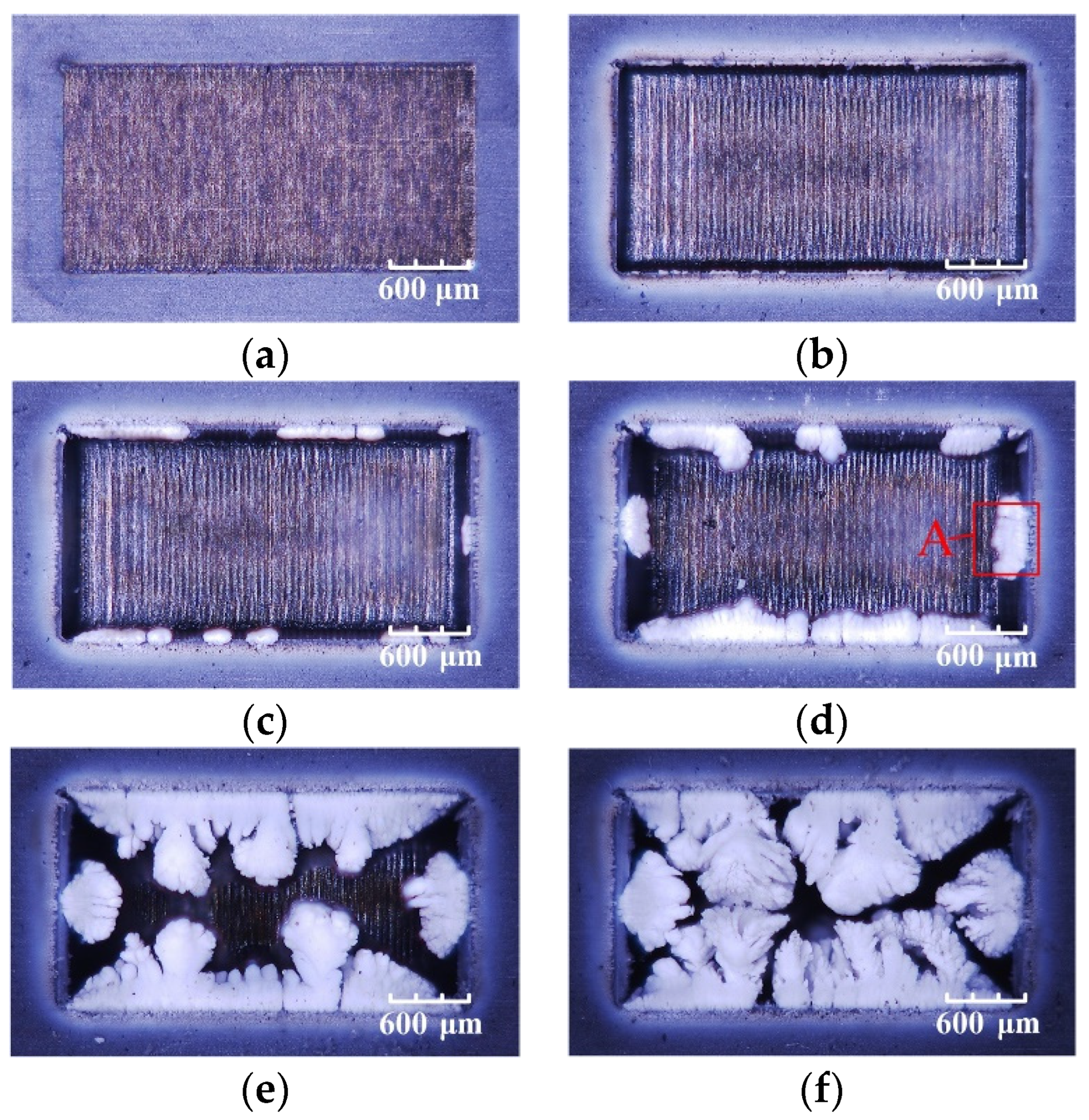
Figure 3 shows the workpiece morphology prior to cleaning after conventional laser processing. Each image shows the material after being processed a different amount of times. In each experiment, the processing area of the groove was 1.5 mm × 3 mm. When the material was processed only 1 time, the material was obviously removed and the outline of the groove was clearly visible, as shown in Figure 3a. When the processing time increased to 50 times, the non-processing area around the groove became white, as shown in Figure 3b. With the continuous increase of processing scans, white products increased and clumped at local contours and gradually extended to the center of the groove (Figure 3c–e). When the processing times was 400 times, white products almost covered the entire area of the groove (Figure 3f). From the magnification of area A in Figure 3d, it can be observed that the white products were granular in the non-processing area outside of the groove, and extended to the processing area in a cluster, as shown in Figure 4.
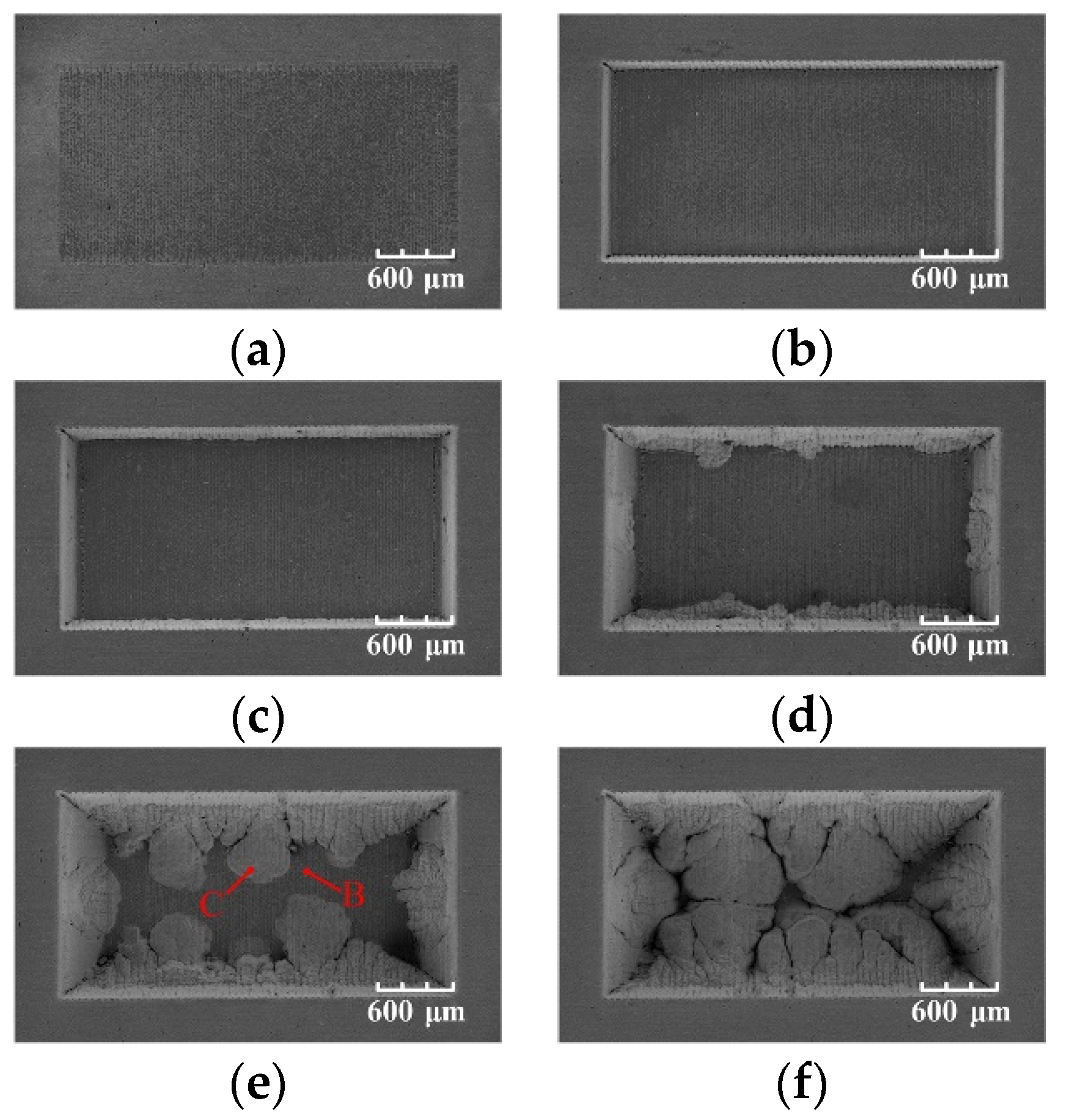
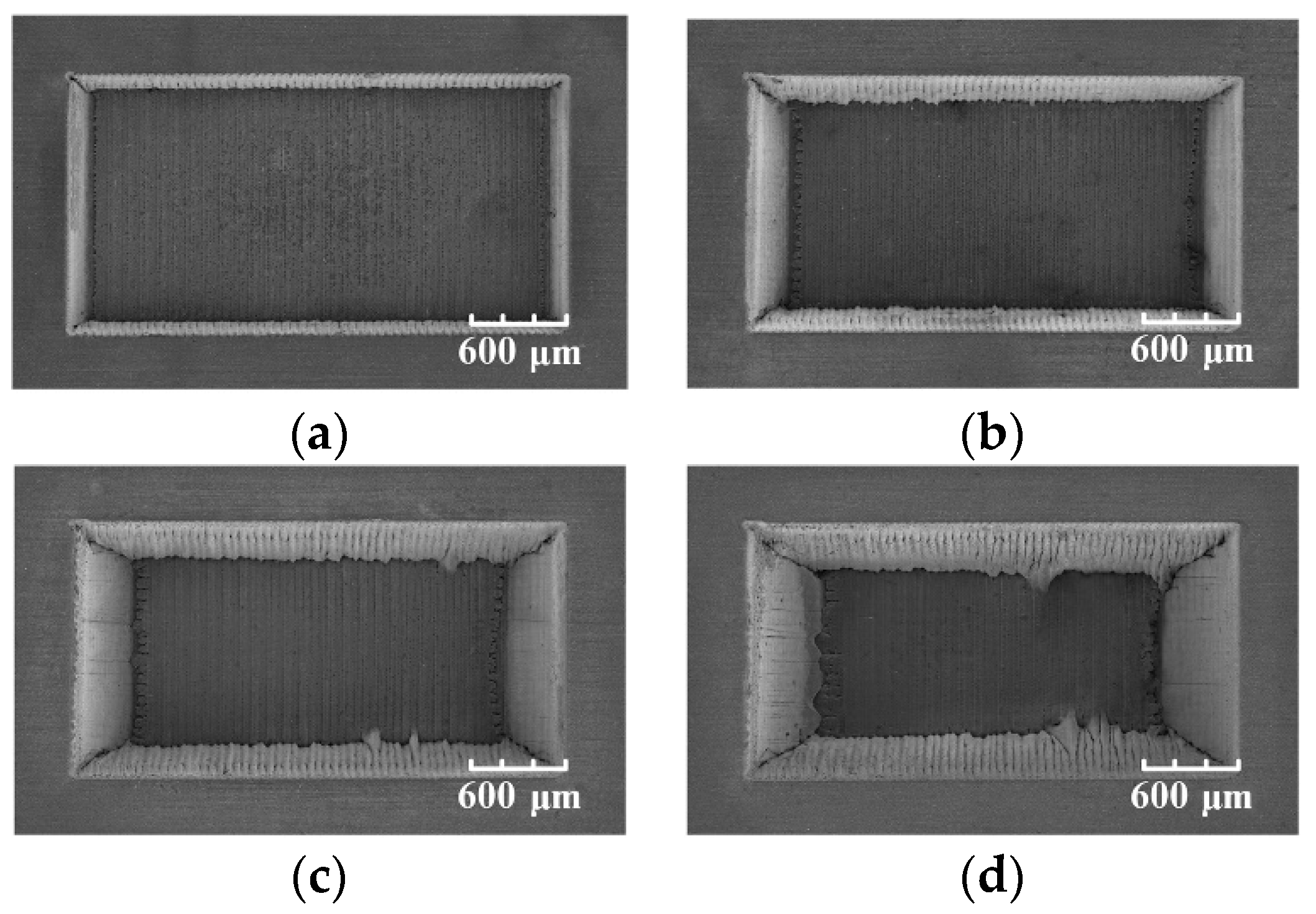
To observe the morphology of the workpiece under the white products, processed workpieces were cleaned in ethanol by ultrasound before SEM testing, and the results are shown in Figure 5. When the material was processed less than 100 times, workpiece surfaces were free of detritus, and the forming quality of the groove structure was excellent, indicating that the silicon carbide material was removed normally (Figure 5a–c). However, when the workpiece was processed 200 times, undesired deposits appeared on the sidewalls of the groove (Figure 5d). This can be explained by the presence of the white products shielding the material from the laser energy, and the deposits were melted and recast. It can also be seen in Figure 5d–f that the recast molten deposits increased with processing times, and the distribution of deposits corresponded to the distribution of the cluster products.
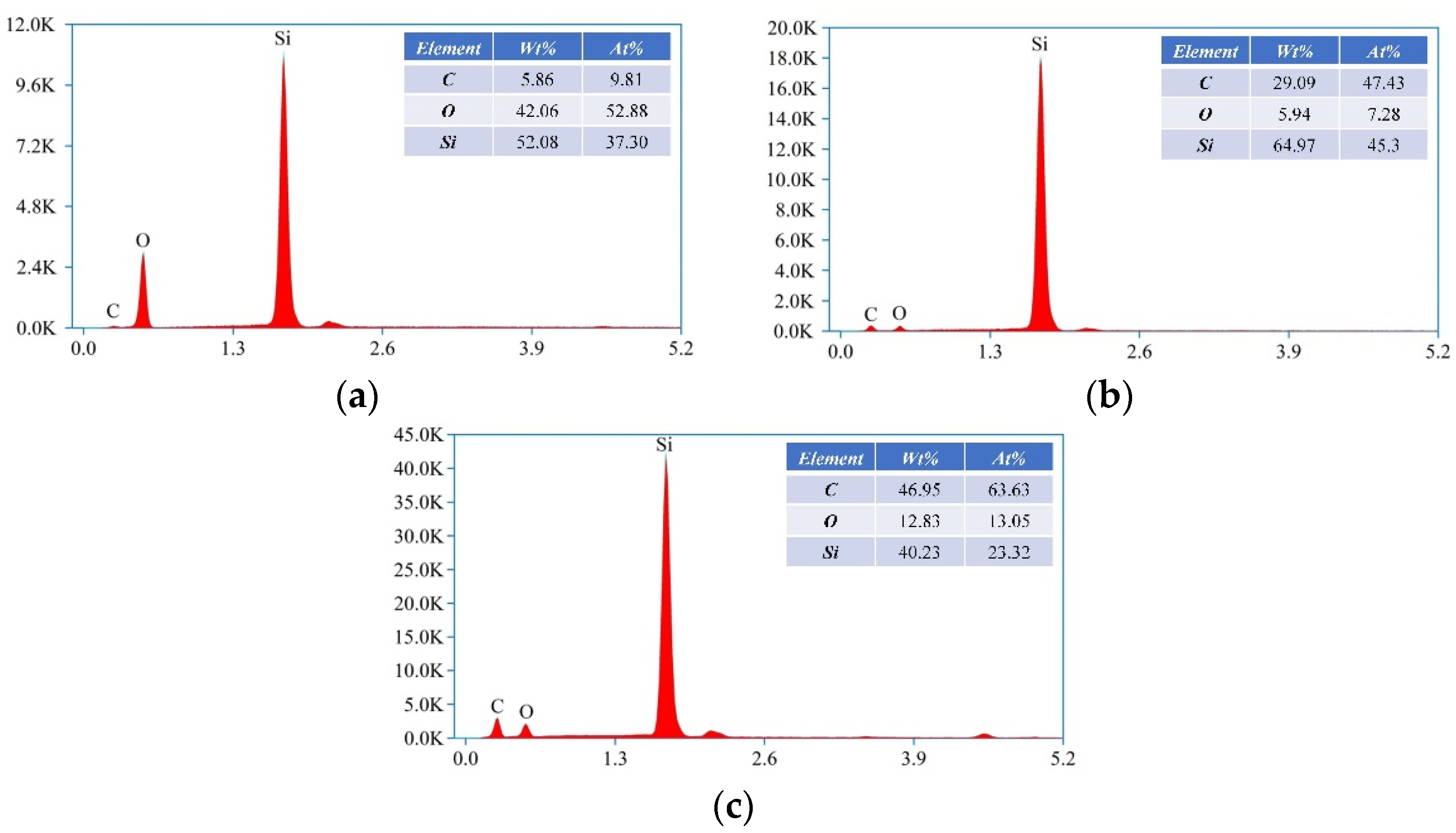
Next, the components of the different processed surfaces shown in Figure 5e were measured by EDS, and the white products on the workpiece surface before cleaning were also collected for EDS measurement. From Figure 6a, it can be concluded that the white products covered on the workpiece surface mainly consisted of Si and O, and also small amounts of C. Therefore, it can be inferred that the white products were mainly SiO2 and a small amount of SiC. The normally processed smooth surface at point B in Figure 5e contained a small amount of oxygen, as shown in Figure 6b, which was due to the oxidation reaction between the material and air during processing. For the surface of the recast deposit at point C in Figure 5e, the main components were C and Si. Therefore, the recast deposit was mainly SiC.

3.2. Groove Structures Processed with Different Processing Times by Blowing-Assisted Laser Processing

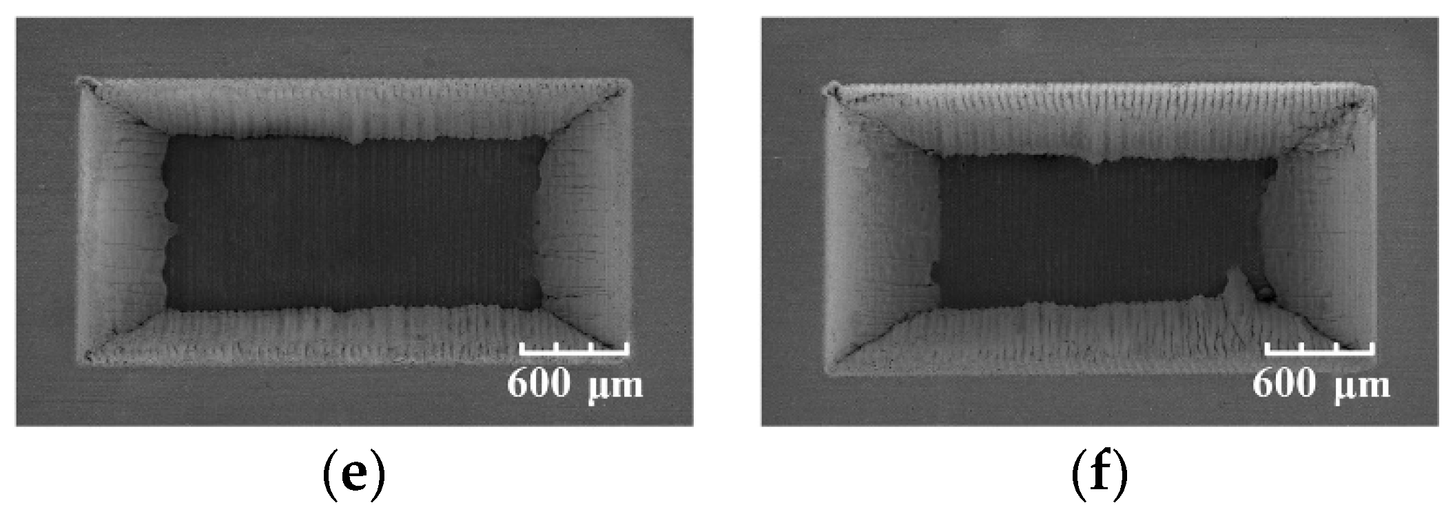
In this section, the groove structures were processed 100 times, 200 times, 300 times, 400 times, 500 times, and 600 times by a blowing-assisted nanosecond laser. The processing area was also 1.5 mm × 3 mm in each experiment, and the morphology of workpieces after cleaning were observed by SEM, as shown in Figure 7. Different from the performance of conventional laser processing, with the increase of processing times, there was no excess melt deposit in groove structures processed by the blowing-assisted laser. Even after processing 600 times, the bottom of the groove was still flat and the quality of the groove was good, indicating that the products had no influence on the processing area in the blowing-assisted laser of silicon carbide. From the above experiment results, it can be concluded that blowing can effectively improve the processing depth and processing quality of groove structures processed by nanosecond laser.

3.3. Grooves of Different Widths Processed by Conventional and Blowing-Assisted Laser Processing

The comparative experiments of conventional and blowing-assisted laser processing were carried out, in which groove structures of different widths (0.6 mm, 0.8 mm, and 1 mm) were processed by the above two methods. In each experiment, the groove structure was processed the same number of times (200 times), with the same parameters were listed in Table 2. As shown in Figure 8, the accumulation of white products was increasingly severe with the decrease of processing width in conventional laser processing. When the processing width was 0.6 mm, the white product almost extended from both sides to the center of the groove (Figure 8c). From the SEM of the grooves in Figure 9, it can be found that for the narrower groove structure, the molten deposit increased significantly with the decrease of processing width, and the processing quality of the groove was also worsened (Figure 9c). The processing results indicated that the conventional nanosecond laser was limited in the processing of microstructures of silicon carbide material.
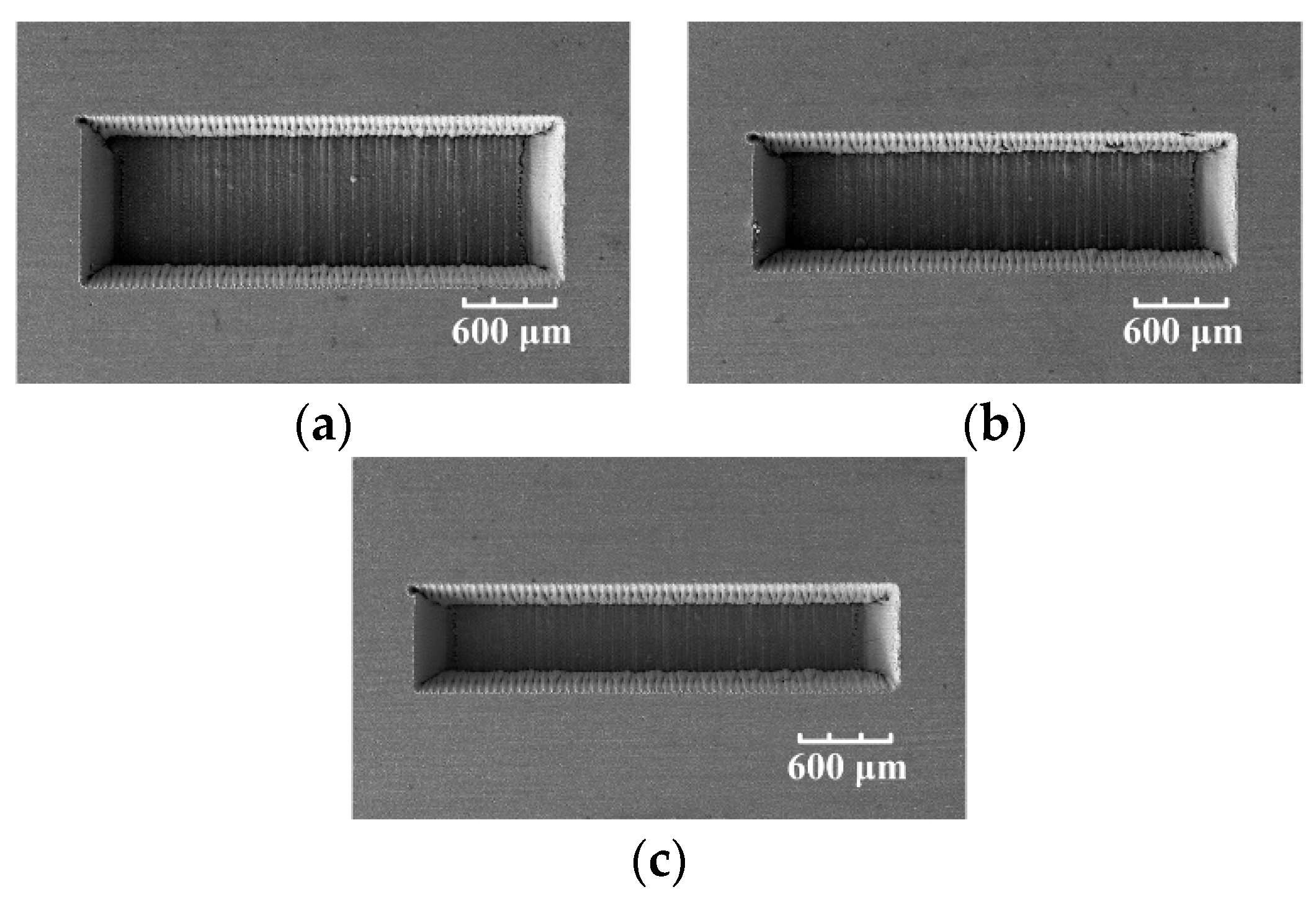
As shown in Figure 10, the narrower groove structure processed by the blowing-assisted laser, are clearly better than that of the conventional laser processing shown in Figure 9. With the reduction of the processing width of the blowing-assisted laser, excess melt deposition did not occur at the side wall of the groove. Even when the processing width was reduced to 0.6 mm, the excellent processing quality could still be obtained, indicating that blowing is helpful to improve the laser’s ability to machine narrower groove structures.

4. Discussion on Array Micro Grooves Processing

Nanosecond pulse lasers are a type of short pulse laser. In the process of material removal, the laser energy in the processing area can cause the matrix material to decompose and sublimate. As shown in Figure 11a, in conventional laser processing, some of the SiC material is sublimated into a gaseous form of SiC(g) with the action of the laser, and some of the SiC material was decomposed into Si(g) and C(g) [24]. The SiC (g) and Si(g) reacted with O2 to generate SiO2(g), which solidified at room temperature. The C(g) reacted with oxygen in the air to generate CO2 and CO gas during the processing. In the conventional nanosecond laser processing, the ablation reactions were as follows:
SiC(s) = SiC(g)
SiC(s) = Si(g) + C(g)
2SiC(s) + 3O2(g) = 2SiO2(g) + 2CO2(g)
Si(s) + O2(g) = SiO2(s)
C(g) + O2(g) = CO2(g)
2C(g) + O2(g) = 2CO(g)
In the bottom of the grooves in the processing area, the laser energy was enough to vaporize the material, and the gaseous products diffused to the outside of the groove and solidified. As shown in Figure 3, oxidation products firstly accumulated around the groove. With the increase of processing times, the oxidation products spread to the center of the groove. Unfortunately, the accumulated products could shield part of the laser energy, and this material was melted and recast. As a result, the poor processing quality was obtained.
In blowing-assisted laser processing, silicon carbide material was processed normally by the laser, and oxidation products were also formed. As shown in Figure 11b, with the assistance of blowing, the oxidation products could be blown away from processing area. There were only a small amount of products near the groove, which would not affect the processing. With the increase of processing depth and the decrease of processing width of the groove structures, the blowing also effectively removed the products, thus avoiding the accumulation of products in the processing area. Therefore, deeper and narrower groove structures of good processing quality could be obtained by blowing-assisted laser processing. In addition, compared with conventional laser processing, waste products could be removed from the processing area more quickly before they had a chance to react, enabling the blowing-assisted laser processing to obtain higher processing efficiency. To further verify that blowing can improve the laser processing capability of silicon carbide, array microgroove microstructures of 1 mm × 1 mm were processed 100 times, 150 times, and 200 times by blowing-assisted laser processing. As shown in Figure 12, the contour of array grooves were clear and the bottom of the groove structures were bright without molten deposits. From the cross-sectional profile, it can be found that the depth of the groove structures gradually increased with the increase of processing times. The processing depth of 1 mm × 1 mm array grooves can be 0.658 mm when processed by the blowing-assisted laser processing 200 times. It can be concluded that blowing-assisted laser processing is more suitable for the processing of microstructures on silicon carbide materials, compared with the conventional laser processing.

5. Conclusions

In this paper, the laser processing of groove structures on silicon carbide surfaces was studied, blowing-assisted laser processing was proposed to improve processing quality of microstructures, and comparative experiments between conventional and blowing-assisted laser processing of groove structures was carried out. The specific conclusions are summarized as follows:
(1)
In conventional laser processing of silicon carbide material, white silicon dioxide products form and accumulate around the processing area with the increase of processing times, which can hinder further material removal and affect the processing quality of groove structures.
(2)
Blowing assistance can remove the oxidation products from the processing area to avoid accumulation and improve the laser processing capability of microstructures. Compared with conventional laser processing, blowing-assisted laser processing can machine deeper and narrower groove structures with higher quality.
(3)
Array structures of 1 mm × 1 mm × 0.658 mm can be processed on silicon carbide surfaces by a nanosecond laser assisted by blowing.
(4)
The influence of blowing on the thermodynamic equilibrium of ablation reactions of silicon carbide requires further analysis in the future.

Author Contributions

Conceptualization, S.Z., B.H.; Investigation, J.L., J.Y.; Writing—original draft preparation, J.L., B.H.; Supervision, G.C.; Project administration, G.C. All authors have read and agreed to the published version of the manuscript.

Funding

This research received no external funding.

Informed Consent Statement

Informed consent was obtained from all subjects involved in the study, and written informed consent has been obtained from the patients to publish this paper.

Conflicts of Interest

The authors declare no conflict of interest.

References

  1. Sharma, S.K.; Kumar, B.; Kim, Y.W. Tribological behavior of silicon carbide ceramics—A review. J. Korean Ceram. Soc. 2016, 53, 581–596. [Google Scholar] [CrossRef] [Green Version]
  2. Gao, S.; Han, Q.k.; Zhang, X.N.; Pennacchi, P.; Chu, F.L. Ultra-high-speed hybrid ceramic triboelectric bearing with real-time dynamic instability monitoring. Nano Energy 2022, 103, 107759. [Google Scholar] [CrossRef]
  3. Zhang, Z.Y.; Yang, X.; Zheng, L.G.; Xue, D.L. High-performance grinding of a 2-m scale silicon carbide mirror blank for the space-based telescope. Int. J. Adv. Manuf. Technol. 2017, 89, 463–473. [Google Scholar] [CrossRef]
  4. Diaz, O.G.; Luna, G.G.; Liao, Z.; Axinte, D. The new challenges of machining Ceramic Matrix Composites (CMCs): Review of surface integrity. Int. J. Mach. Tools Manuf. 2019, 139, 24–36. [Google Scholar] [CrossRef]
  5. Kildemo, M. Optical properties of silicon carbide polytypes below and around bandgap. Thin. Solid. Films. 2004, 455, 187–195. [Google Scholar] [CrossRef]
  6. Abrego Serrano, P.A.; Kim, M.; Kim, D.R.; Kim, D.H.; Kim, G.H.; Ahn, S.H. Spherical mirror and surface patterning on silicon carbide (SiC) by material removal rate enhancement using CO2 laser assisted polishing. Int. J. Precis. Eng. Manuf. 2020, 21, 775–785. [Google Scholar] [CrossRef]
  7. Pawar, P.; Ballav, R.; Kumar, A. Machining processes of silicon carbide: A review. Rev. Adv. Mater. Sci. 2017, 51, 62–76. [Google Scholar]
  8. You, K.Y.; Yan, G.P.; Luo, X.C.; Michael, D.G.; Fang, F.Z. Advances in laser-assisted machining of hard and brittle materials. J. Manuf. Process. 2020, 58, 677–692. [Google Scholar] [CrossRef]
  9. Samant, A.N.; Dahotre, N.B. Laser machining of structural ceramics—A review. J. Eur. Ceram. Soc. 2009, 29, 969–993. [Google Scholar] [CrossRef]
  10. Pecholt, B.; Gupta, S.; Molian, P. Review of laser microscale processing of silicon carbide. J. Laser. Appl. 2011, 23, 012008. [Google Scholar] [CrossRef]
  11. Pan, Y.C.; Zhan, Q.L.; Guo, B.; Long, Y.T. High-efficiency machining of silicon carbide Fresnel micro-structure based on improved laser scanning contour ablation method with continuously variable federate. Ceram. Int. 2021, 47, 4062–4075. [Google Scholar] [CrossRef]
  12. Zhai, Z.Y.; Wang, W.J.; Mei, X.S.; Li, M.; Cui, J.L.; Wang, F.C.; Pan, A.F. Effect of the surface microstructure ablated by femtosecond laser on the bonding strength of EBCs for SiC/SiC composites. Opt. Commun. 2018, 424, 137–144. [Google Scholar] [CrossRef]
  13. Li, M.J.; Li, S.; Yang, X.J.; Zhang, Y.; Liang, Z.C. Fiber laser cutting of CFRP laminates with single-and multi-pass strategy: A feasibility study. Opt. Laser. Technol. 2018, 107, 443–453. [Google Scholar] [CrossRef]
  14. Pecholt, B.; Vendan, M.; Dong, Y.Y.; Molian, P. Ultrafast laser micromachining of 3C-SiC thin films for MEMS device fabrication. Int. J. Adv. Manuf. Technol. 2008, 39, 239–250. [Google Scholar] [CrossRef]
  15. Dong, Y.Y.; Nair, R.; Molian, R.; Molian, P. Femtosecond-pulsed laser micromachining of a 4H–SiC wafer for MEMS pressure sensor diaphragms and via holes. J. Micromech. Microeng. 2008, 035022. [Google Scholar] [CrossRef]
  16. Tong, Y.G.; Bai, S.X.; Zhang, H.; Ye, Y.C. Laser ablation behavior and mechanism of C/SiC composite. Ceram. Int. 2013, 39, 6813–6820. [Google Scholar] [CrossRef]
  17. Zhai, Z.Y.; Chen, W.; Zhang, Y.C.; Cui, Y.H.; Zeng, Q.R. Investigations on the oxidation phenomenon of SiC/SiC fabricated by high repetition frequency femtosecond laser. Appl. Surf. Sci. 2020, 502, 144131. [Google Scholar] [CrossRef]
  18. Jiao, H.W.; Chen, B.; Deng, Z.H. Influence of laser parameters on processing microgrooves of 2.5-dimensional C/SiC composites via nanosecond laser. Int. J. Adv. Manuf. Tech. 2022, 118, 85–101. [Google Scholar] [CrossRef]
  19. Cheong, H.G.; Chu, C.N.; Kwon, K.K.; Song, K.Y. Micro-structuring silicon compound ceramics using nanosecond pulsed laser assisted by hydrothermal reaction. J. Manuf. Process. 2020, 50, 34–46. [Google Scholar] [CrossRef]
  20. Iwatani, N.; Doan, H.D.; Fushinobu, K. Optimization of near-infrared laser drilling of silicon carbide under water. Int. J. Heat Mass Transf. 2014, 71, 515–520. [Google Scholar] [CrossRef]
  21. Khuat, V.; Ma, Y.C.; Si, J.H.; Chen, T.; Chen, F.; Hou, X. Fabrication of through holes in silicon carbide using femtosecond laser irradiation and acid etching. Appl. Surf. Sci. 2014, 289, 529–532. [Google Scholar] [CrossRef]
  22. Srinivasu, D.S.; Axinte, D.A.; Shipway, P.H.; Folkes, J. Influence of kinematic operating parameters on kerf geometry in abrasive waterjet machining of silicon carbide ceramics. Int. J. Mach. Tool. Manuf. 2009, 49, 1077–1088. [Google Scholar] [CrossRef]
  23. Liu, Y.; Wei, M.R.; Zhang, T.; Qiao, H.C.; Li, H. Overview on the development and critical issues of water jet guided laser machining technology. Opt. Laser Technol. 2021, 137, 106820. [Google Scholar] [CrossRef]
  24. Feng, S.C.; Huang, C.Z.; Wang, J.; Zhu, H.T. Material removal of single crystal 4H-SiC wafers in hybrid laser-waterjet micromachining process. Mat. Sci. Semicond. Process. 2018, 82, 112–125. [Google Scholar] [CrossRef]
Figure 1. Schematic diagram of blowing-assisted laser processing.
Applsci 12 11234 g001
Figure 2. Schematic of the laser processing path.
Applsci 12 11234 g002
Figure 3. Workpiece morphology processed a different number of times by conventional laser processing prior to cleaning: (a) 1 time, (b) 50 times, (c) 100 times, (d) 200 times, (e) 300 times, (f) 400 times.
Applsci 12 11234 g003
Figure 4. Magnification of area A in Figure 3d.
Applsci 12 11234 g004
Figure 5. SEM of workpieces processed a different number of times by conventional laser processing after cleaning: (a) 1 time, (b) 50 times, (c) 100 times, (d) 200 times, (e) 300 times, (f) 400 times, B in (e) was the surface of normal machining, C in (e) was the surface of deposit.
Applsci 12 11234 g005
Figure 6. EDS spectra of different processed surfaces: (a) white products, (b) normal processing surface at point B, (c) deposit surface at point C.
Applsci 12 11234 g006
Figure 7. SEM of workpieces processed a different number of times by a blowing-assisted laser after ultrasonic cleaning: (a) 100 times, (b) 200 times, (c) 300 times, (d) 400 times, (e) 500 times, (f) 600 times.
Applsci 12 11234 g007aApplsci 12 11234 g007b
Figure 8. Workpieces of different widths processed by conventional laser processing, shown after ultrasonic cleaning: (a) width of 1 mm, (b) width of 0.8 mm, (c) width of 0.6 mm.
Applsci 12 11234 g008
Figure 9. SEM of workpieces of different widths processed by conventional laser processing, shown after ultrasonic cleaning: (a) width of 1 mm, (b) width of 0.8 mm, (c) width of 0.6 mm.
Applsci 12 11234 g009
Figure 10. SEM of workpieces of different widths processed by blowing-assisted laser processing, shown after ultrasonic cleaning: (a) width of 1 mm, (b) width of 0.8 mm, (c) width of 0.6 mm.
Applsci 12 11234 g010
Figure 11. Schematic of material removal in the fiber nanosecond laser processing of SiC material: (a) conventional laser processing, (b) blowing-assisted laser processing.
Applsci 12 11234 g011
Figure 12. Surface and cross-section of array grooves of 1 mm × 1 mm processed with different times by blowing-assisted laser processing. (a) 100 times, (b) 150 times, (c) 200 times.
Applsci 12 11234 g012
Table 1. Parameters of experimental samples.
Density
(g/cm3)
Bending Strength
(MPa)
Rockwell Hardness
(HRA)
Thermal Conductivity
(W/mK)
Elastic Modulus
(GPa)
3.1240093148415
Table 2. Parameters in laser processing experiments.
ParameterConventionalBlowing-Assisted
Scanning speed500 mm/s
Pulse frequency20 kHz
Pulse width100 ns
The wavelength of laser1064 nm
Laser power18 W
Scanning processing times1, 50, 100, 200, 300, 400100, 200, 300, 400, 500, 600
Publisher’s Note: MDPI stays neutral with regard to jurisdictional claims in published maps and institutional affiliations.