Abstract
The paper analyzes the image quality in augmented reality display based on holographic waveguides. Brightness, brightness non-uniformity, image noise, etc., depend on the parameters of the waveguide substrate, the configuration, and the relief shape of diffraction optical elements. The optimal structure of holographic waveguides obtained by analog holography has been studied. The presented recommendations to achieve the best image quality are based on experimental results for different configurations of holographic waveguides.
1. Introduction
The growing computing power of today’s devices and everyday digitalization have brought augmented and virtual reality (AR and VR) technologies to a new level. As a result, it can go beyond the entertainment industry and cover a wide range of human activities. In this case, when implementing AR and VR technology, attention should be paid not only to software but also to hardware, which allows to visualize computer synthesized images and objects. In practice, the hardware of most solutions is represented by wearable glasses (or so-called head-mounted displays) with a head- or belt-mounted control and power unit [1,2]. Currently, many research groups around the globe are developing AR methods to display synthesized images superimposed on real-world objects. These are see-through half-reflective AR mirror displays [3,4], off-axis spherical reflective combiners [5,6], and planar optical waveguides, which are subdivided into composite prismatic [7,8] and holographic [9,10,11]. Analysis of various methods in this field shows that holographic waveguide technology is currently in the lead in terms of the best optical parameters, such as the eye box, the field of view, and the exit pupil size [12,13,14,15].
A holographic waveguide is a plane-parallel [16,17] or curved [18] glass plate in which light is propagated by total internal reflection (TIR). Diffractive optical elements (DOEs) are used to input radiation into the waveguide, as well as to redirect and output radiation into the observer’s eye. In this case, DOEs are a set of relief-phase diffraction gratings [19,20] or volume gratings [13,21] formed on the surface [11,13] or inside the waveguide [21], respectively. Many companies such as Microsoft HoloLens, Magic Leap, WaveOptics, Dispelix, etc. are developing and manufacturing AR HMDs [12]. Holographic waveguides in such devices provide an angular field of view of about 30−55 degrees and the size of the exit pupil is 10−20 mm [11].
Holographic waveguides are mostly based on relief-phase [19,20] or photopolymer [13,22] diffraction gratings, which operate in the Raman-Nath diffraction mode, but there are also solutions based on the Bragg diffraction mode [21,23]. In the case of an analog quasi-sinusoidal relief profile, the gratings have a diffraction efficiency of up to 34%; in the case of a binary (rectangular) relief profile, they have a diffraction efficiency of up to 41% [24]; in case of a slanted relief profile, they have a diffraction efficiency over 80% [20], acquiring the properties of Bragg gratings. The manufacturing of slanted diffraction gratings requires a complex technological process based on reactive ion etching and nanoimprint lithography [25]. This paper investigates holographic waveguides based on analog photoresist diffraction gratings with a quasi-sinusoidal relief profile.
Image quality formed by holographic waveguides essentially differs from the image quality formed by standard projectors. This paper analyzes the influence of the DOEs configuration on the image quality, expressed by the presence of chromatic aberrations and different brightness uniformity artifacts. The research aims to ensure the quality of image projection through a holographic waveguide obtained using analog technology (holography). The paper presents various configurations of holographic waveguides and provides recommendations for those that meet the quality requirements of the output image.
2. Materials and Methods
2.1. General Principles for the Holographic Waveguide Design
The optical systems of HMD devices contain two main functional parts: the optical engine or image generation module, which is a compact projector; and the so-called transparent display, i.e., the optical component that transmits images from the projector to the observer’s eye. AR display based on the holographic waveguide is notable for its field of view above 50° [11,12,26]. The angular field is provided by the high refractive index of the glass substrate, which is responsible for the cone of TIR beams in the substrate, and the presence of several waveguide plates for different spectral channels (e.g., RGB) needed to form a color image. For the light to be transmitted effectively through the plate to the eye, the field of view must be divided by angle and spectrum across several plates [27,28]. Each of the plates propagates a certain portion of the light, as shown in Figure 1.
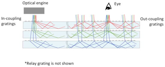
Figure 1.
Scheme of the full color transparent display based on planar holographic waveguides.
Figure 1 illustrates a three-layer holographic waveguide. For each spectral channel, the collimated beams from the projector diffract into the substrate (+1 order of diffraction) and propagate inside by TIR means. For this, the diffraction angle must be larger than the TIR angle. Consequently, the greater the refractive index of the plate, the greater the potential angular field of view to be transmitted. The second condition applied to the diffraction angle inside the substrate is related to the pupil size and substrate thickness, and hence to the maximum pupil spacing during pupil replication. The light beams for each of the spectral channels, move along the corresponding direction in the light guide according to the grating equation
where ntr is the refractive index of the waveguide, φm is the diffraction angle (from the normal), ninc is the refractive index of the media of the incident light (air), θ is the incident angle, m is the order of diffraction, λ is the wavelength, d is the period of the diffraction grating.
The output DOE (Figure 1) which breaks the TIR condition to output the light, is located near the eye. The light beams leave the waveguide in the same direction as the incident beams. Using a symmetrical configuration of the input/output DOE is a simple method of compensating for the spectral misalignment in the image.
Each of the transmitting diffraction gratings in the three-layer holographic waveguide satisfies the coordinated propagation angles in the waveguide for red, green, and blue radiation. Figure 1 is only a schematic representation of the principle of radiation input and output relative to the plate. Since the surface diffraction gratings are non-selective and operate in the Raman-Nath diffraction mode according to equation (1), light with any incident angle for one wavelength can partially diffract on a grating designed for another wavelength, as described in [29]. The color channels may be partially mixed, but the final image is unaffected by that spectral overlapping. The principles of diffraction grating calculation are described in detail [2,30]. Therefore, there can be two or three plates depending on the spectrally transmitted angular composition. This effect is visualized in more detail in Section 2.2.
To provide the size of the exit pupil, which is many times larger than the entrance pupil, an intermediate DOE, relay grating, is placed between the input and output DOEs. DOE configurations that help to achieve two-dimensional eye box expansion, required for most AR displays, are described in [29] and presented in Figure 2. It is often recommended to make the output element DOE3 with variable diffraction efficiency increase in the direction of propagation. This condition allows you to align the brightness of the output image within the field of view and the exit pupil.
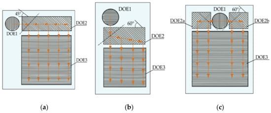
Figure 2.
2D pupil replication layouts for planar holographic waveguides: (a) based on an odd number of first-order diffractions; (b) based on an even number of first-order diffractions; (c) dual-channel exit pupil expansion .
In this work, various configurations of waveguides with two-dimensional eye box based on analog relief-phase gratings are studied. On the one hand, a low diffraction efficiency of the output holographic DOE (less than 25%) compared to the lithographic one reduces the overall waveguide efficiency, while on the other hand, it gives room for experiments on waveguides to eliminate various artifacts in the image. Analog diffraction gratings have less freedom in controlling the parameters of the relief profile compared to lithographic and etching solutions, but more possibilities in terms of production speed and accessibility.
2.2. Diffraction Analysis for the Waveguide Gratings
To analyze the correct profile height, analog grating diffraction was modeled using a Matlab numerical solution based on RCWA (rigorous coupled wave analysis). Figure 3 shows the resulting characteristics of diffraction efficiency via relief height.
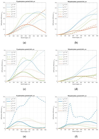
Figure 3.
Dependences of diffraction efficiency (η−1) on the relief height of holographic diffraction grating for three color channels according to Table 1. RGB diffraction analysis: for the red channel grating in TE polarization (a) and TM polarization (b); for the green channel grating in TE polarization (c) and TM polarization (d); for the blue channel grating in TE polarization (e) and TM polarization (f). Plots are given for angles of incidence 0 and 15 degrees combined for two perpendicular polarizations of incident light.
RCWA is one of the most popular and efficient methods to solve the diffraction problem since the 1980s [31,32]. The code calculates the interaction of a plane electromagnetic wave with the periodic structure providing the diffraction efficiencies of all existing reflected and transmitted diffraction orders.
As initial data for the calculation, the incident wave has a unity amplitude of electric vector E and zero phases. Since the wave field is polarization-dependent, two conditions were analyzed: TE polarization, as Figure 4a illustrates, and TE polarization, as shown in Figure 4b. Unpolarized light is equivalent to the average of TE and TM diffraction efficiency. In this case, the x-axis corresponds to the grating vector, the y-axis corresponds to the lines of the diffraction grating, and the z-axis is perpendicular to the plane of the diffraction grating. The radiation wavelengths are λB = 0.459 μm, λG = 0.53 μm, and λR = 0.625 μm.
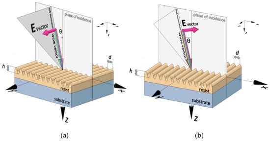
Figure 4.
Illumination geometry for TE polarization (a) and TM polarization (b): E—vector of electric field (magnetic field is not shown), θ—angle of incidence, d—diffraction grating period, h—relief height.
Table 1 combines not only the parameters for modeling but also the general parameters of the waveguide. The substrate material (F6) determines the minimum TIR angle for light propagation in the waveguide. The recording angle is angle α in Figure 5a—the angle between the normal to the grating surface and the angle of incidence of the interfering wave, which will be described in more detail in the following section.

Table 1.
Parameters of the coupling gratings.
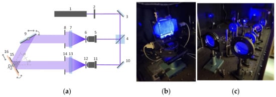
Figure 5.
(a) The scheme of the recording setup: 1—He-Cd laser; 2—shutter; 3,10—mirrors; 4—beam splitter; 5, 11—micro objectives; 6, 12—pinhole diaphragm; 7, 13—collimating lenses; 8, 14—field diaphragm; 9—mirror placed on linear and angular positioners; 15—diaphragm corresponding with coupler shape; 16—waveguide plate with photoresist layer placed on linear and angular positioners, and rotation stage in the waveguide plane. (b) Photo of the recording area. (c) Photo of the setup (components 4–14).
The diffraction distribution in –1 diffraction order was calculated for two incidence conditions from cover to substrate: normal to the grating plane and oblique at the angle of 15°. The dielectric permittivity of the media was specified as follows. The cover zone corresponds to air, substrate zone corresponds to F6. The structure zone is resin S1813 having dielectric permittivity distribution defined with sinusoidal profile functions. As for the calculation parameter, the number of harmonics in the expansion series is N = 16 (the total number 2N + 1 = 33) for every case.
The resulting data represents the performances of diffraction efficiencies in −1 order (η−1) depending on grating depth h in the range from 0 to the grating period. To maximize the diffraction efficiency across the angular field of view it was decided to use gratings with a profile height of 100 to 150 nm. In the following experiments, surface relief was about 120 nm. This condition, firstly, is consistent with the equalization of diffraction efficiency for different incidence angles. Secondly, at such a profile height the property of dependence of diffraction efficiency on polarization is less apparent, as illustrated by Figure 3. Thirdly, when holographic diffraction gratings are not designed to maximize diffraction efficiency, various interference artifacts at the recording stage have less effect on the quality of the diffracted wavefront across the field. Experimental confirmation of these statements is described in the following sections.
2.3. Recording Setup
The transmission relief-phase diffraction gratings on the surface of the waveguide substrate were recorded by analog holography method on a vibration-isolated stand, i.e., by dividing the laser beam into reference and subject branches and exposure of the photosensitive material with the resulting interference field. The scheme of the stand is shown in Figure 5.
He-Cd laser HCL-100V(I) (PLASMA JSC, Ryazan, Russia) 1 was used as a source of continuous-wave coherent radiation, a wavelength of 0.44 μm, and a power of 150 mW. The laser is followed by a shutter 2, which provides the necessary exposure time, i.e., the time of illumination of the photoresist by laser radiation. Then radiation is divided into two parts (two branches) by beam splitting cube 4. Mirrors 3 and 10 are for breaking the optical axis and redirection of light propagation direction by 90 degrees. In the case of manufacturing a DOE as a diffraction grating, it is necessary to superimpose two collimated light beams. For this purpose, all branch filtering systems were used as a combination of microobjective 5 (11) in the reverse beam path and pinhole diaphragm 6 (12), and then collimating lens 7 (13), which together create a beam expander unit. The presence of the point aperture (10−15 microns in diameter) is necessary to spatially filter the radiation and to increase the uniformity of illumination within the beam aperture of lenses 7 and 13. The field apertures 8 and 14 are set to additionally screen out the recording area.
Mirror 9 provides the required recording angle of DOE (angle α in Figure 5a). Two collimated beams are superimposed in the plane of the photoresist layer of the waveguide 15, which results in an interference pattern of straight fringes. To ensure the angle of convergence of the interfering beams and to adjust the setup it is necessary to install waveguide 15 on the linear and rotary translators. As the holographic waveguide has several composed DOEs, when recording each of them on the above-described setup the registration plate (waveguide) is rotated to provide the orientation of the diffraction grating. The aperture is used to provide the geometry configuration and size of the DOE. Shipley’s 1813 photoresist was used as the photosensitive medium. AZ303 was used as a developer, the developing time was ~25 s when the developer was prepared in the proportion of 1:4 with distilled water. The resulting holographic waveguides in this work were an assembly of four stacked plates (1 mm thick), three of them were plates with diffraction gratings for RGB, and the fourth was a safety glass.
3. Results
To study the quality of the projected image, color reproduction, and brightness non-uniformity [33,34,35,36] holographic waveguides with different DOE configurations were made for a three-channel RGB system. As described above, in this implementation the holographic waveguides consist of three combined substrates for each of the RGB colors. The diffraction grating periods are different for different color channels, but the shape and size of the DOEs are the same.
For each color channel, DOEs consisting of several diffraction gratings with the same periods but different orientation directions were manufactured. This essentially simplifies the recording setup and also makes it possible to obtain higher values of periods than, for example, in the schemes shown in Figure 2a,c, and described in [20,30], respectively. Below is a description of the different DOE configurations tested in the experiment.
3.1. First DOE Configuration
The first configuration under study is an analog of the scheme shown in Figure 2c and implements the principle of geometrical separation of the incident light into two parts to increase the size of the angular field of view. The difference between this configuration and the ones proposed in [20,30] is that all three DOEs on the surface of the waveguide have the same period, while the referenced configurations have periods of the input and relay gratings that differ by √2 times. Figure 6 shows the holographic waveguide of the first configuration with the input DOE consisting of the superimposed diffraction gratings, as well as the different orientations of the direction of the diffraction gratings. Due to a symmetrical structure, a higher field of view is provided by dividing the input light into two symmetrical components propagating in the waveguide in opposite directions.
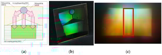
Figure 6.
The first configuration of the holographic waveguide: (a) DOE configuration scheme; (b) photo of a single holographic waveguide; (c) resulting AR image.
In this implementation, the input DOE is a diffraction grating formed by two superimposed one-dimensional diffraction gratings with a 60° angle between the line directions, as the layout in Figure 6a shows. Figure 6b is a photo of a single waveguide with diffraction gratings, recorded in accordance with Figure 5a. When the radiation enters the DOE1 area the diffracted beams propagate towards the DOE2a and DOE2b areas providing the expansion of the exit pupil in the horizontal direction and then due to the diffraction unfolds downwards towards the output DOE3 area. Light diffracted by the output DOE3 exits the plate toward the observer’s eye. At the same time, part of the radiation continues to propagate in the holographic waveguide along the DOE3 area, which provides the exit pupil expansion in the vertical direction.
The resulting field of view is represented by Figure 6c. Two negative factors affecting the quality of the generated AR image were identified in this implementation. Firstly, there is a combinational parasitic periodicity in the horizontal direction within the entire superimposed DOE1 area. Secondly, a sufficiently accurate alignment of DOE1, DOE2a, and 2b is required. The presence of gaps or overlaps in these areas leads to a decrease in diffraction efficiency, resulting in visible dark bands in the output image, as Figure 6c shows. Recording of each diffraction grating on the holographic setup is carried out sequentially using masks (or diaphragms), but even 0.2 mm accuracy of their positioning relative to the plate does not allow getting rid of the above-described effect. It happens due to large angles of convergence of reference and object beams in the recording setup and the final thickness of the mask.
It is experimentally shown that the main disadvantage of the holographic waveguide with the first DOEs configuration is a high brightness non-uniformity of the observed image. A bright vertical stripe is present in the image, caused by diffraction on the superimposed parasitic grating. Some part of the light goes from DOE1 right to DOE3, bypassing the DOE2 area. The width of the stripe in the image corresponds to the diameter of the input pupil. For the first configuration of the holographic waveguide the achieved level of brightness non-uniformity was about 65% because light and dark stripes are explicit in the image.
It is not possible to reduce the diffraction efficiency of the «parasitic» diffraction grating to reduce the brightness of the central stripe in the image because it would as well determine the in-coupling efficiency. That will decrease the brightness of not only the central stripe but also the observed image.
3.2. Second DOE Configuration
The second configuration of the holographic waveguide, proposed and tested, is shown in Figure 7. Such an architecture can be defined as no segmentation, because in the input and relay areas with DOE1, DOE2a and DOE2b have no formal division, and, consequently, no overlapping boundaries. Here, a single area formed by superposing DOE1, DOE2a, and DOE2b areas (Figure 6a) performs as two-dimensional diffraction gratings with a 60° angle between the line directions of the diffraction gratings. DOE1 in Figure 6a is expanded to the areas of DOE2a and DOE2b, as Figure 7a represents.
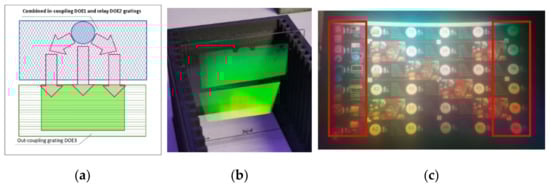
Figure 7.
The second configuration of the holographic waveguide: (a) DOE configuration scheme; (b) photo of a single holographic waveguide; (c) resulting AR image.
The input pupil corresponds with the aperture directly illuminated by the optical engine, and the function of the relay region is performed by its left and right parts outside the input area, respectively.
In such a structure there are no overlapping frames of the input and relay areas with DOEs, and thus one of the factors of possible quality degradation of the image is absent. Due to the superposition of gratings, the resulting diffraction structure begins to outcouple the radiation from the waveguide while horizontal pupil expansion. On the one hand, this contributes to a decrease in the brightness of the central band, since the radiation of the parasitic part does not completely reach the DOE2 region. On the other hand, this leads to direct optical loss, which reduces the overall brightness of the observed image. The optical losses in the side parts of DOE1 are caused by the presence of additional periodicity which is symmetrical to the main one. As Figure 7c shows, the second waveguide configuration has a noticeable decrease in brightness at the edges of the field, but despite all of the above, satisfactory quality of the observed image is achieved. For the second configuration of the holographic waveguide the achieved level of brightness non-uniformity was about 40% because light and dark stripes are explicit in the image.
3.3. Third DOE Configuration
Based on the configurations presented in Figure 6 and Figure 7, a modification of the holographic waveguide shown in Figure 8 was proposed and tested. The central area (the light input) uses a superimposed diffraction structure consisting of two diffraction gratings arranged at the angle of ±60°. The DOE2a and DOE2b at the edges of the waveguide are one-dimensional gratings with direction angles of plus and minus 60°, respectively.
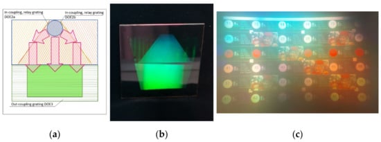
Figure 8.
The third configuration of the holographic waveguide: (a) DOE configuration scheme; (b) photo of a single holographic waveguide; (c) resulting AR image.
The DOE1 input area of the third configuration is combined with a part of the relay grating area, i.e., it is increased practically to the boundary of the DOE3 area, as displayed by Figure 8a. Increasing the area of the input superimposed structure leads to decreasing the observed brightness of the central stripe of the image, as in the above-described case. It is supported by introducing additional optical losses on the superimposed structure due to self-diffraction during propagation towards the DOE3 area.
Relay DOE2a and DOE2b are free from overlapping at the sides and, accordingly, from the presence of parasitic periodicity. Increasing the DOE2a and DOE2b areas will result in decreasing the optical losses, and the slope of their overlapping borders allows for excluding the sharp changes in brightness of the observed image in the horizontal direction. For the third configuration of the holographic waveguide the achieved level of brightness non-uniformity was about 28% because light and dark stripes are explicit in the image (Figure 8c).
Nevertheless, experimental verification of this configuration did not yield significant results, because different parts of the field (different TIR angles in the waveguide) work with different sections of the input and relay DOEs with one or two superimposed gratings in the case of exit pupil expansion along the horizontal coordinate. This feature affects the brightness of these image parts and, therefore, the equal-dimensional brightness of the image.
3.4. Fourth DOE Configuration
To eliminate the drawbacks inherent in the holographic waveguide structures considered above, an implementation of the holographic waveguide shown in Figure 9 was proposed and tested. Here, as in the first configuration shown in Figure 6, there are input DOE1, relay DOE2a, and DOE2b, and output DOE3 recorded separately and overlapped with an accuracy of ±0.2 mm. DOE1 consists of two symmetric (with a vertical axis of symmetry) halves. Each of the halves has its own DOE1a and DOE1b with oblique directions of the lines at the angle of 60° in both structures. This configuration provides the in-coupling of the light in the direction of the relay DOE2a and DOE2b areas.
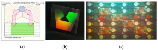
Figure 9.
Fourth configuration of the holographic waveguide: (a) DOE configuration scheme; (b) photo of a single holographic waveguide; (c) resulting AR image.
Experiments with this configuration showed that there is no overlapping structure influencing the in-coupling of the light because this configuration is free of superimposed gratings. The optical efficiency of this configuration is higher than that of the above, but the fabrication requires precise alignment of DOE1 and DOE2 areas since possible overlaps or gaps could lead to dark stripes in the image. For the fourth configuration of the holographic waveguide the achieved level of brightness non-uniformity was about 18%. It should also be noted that five diffraction gratings need to be recorded separately to implement this configuration, which is the largest number among all previous cases.
4. Discussion
Interesting results were obtained during the experiments concerning the arrangement of individual waveguides (for RGB colors) in the stack. There are two options for in-coupling conditions: the photoresist layer with DOEs is located in the direction of light incidence or the light is coming from the substrate. At the same time, inside the stack, the waveguides can be arranged in different ways to protect the photoresist layer from mechanical influences, as, for example, shown in Figure 10a.
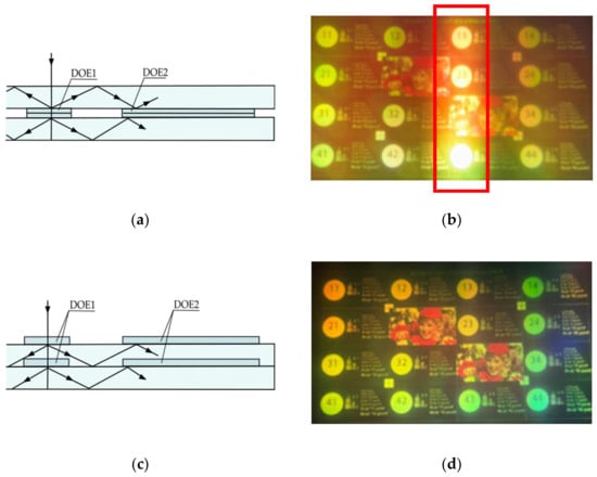
Figure 10.
Options of DOE arrangements in relation to the input light representing the axial vertical section of the waveguide: (a) on the substrate side; (c) on the photoresist side. Examples of resulting images based on the holographic waveguide: (b) for scheme (a); (d) for scheme (c).
The quality of the reproduced image will be affected by the combined structure appearing while a recording of superimposed input DOEs, as shown in Figure 6, Figure 7, Figure 8, and Figure 9. The light in-coupling in two possible arrangements in relation to the input light is illustrated in Figure 10a,c. When the light diffracts on the DOE in the reflection mode (structure glass-resist) it is associated with a greater change in the optical path difference (Figure 10a). In the other case when the light diffracts in transmission mode (structure air-resist) it has a smaller optical path difference.
The stack configuration of Figure 10a provides higher diffraction efficiency and, accordingly, increased brightness of the image, as illustrated by the photo in Figure 10b. Thus, the angular field of view is high and the chromatism is low, but the bright stripe is a significant artifact.
In this connection, it is preferable to choose the arrangement of all the RGB waveguides as in Figure 10c when the side of the photoresist layer faces the input light. An example of the resulting image is shown in Figure 10d. However. this arrangement requires an additional cover substrate to protect the photoresist layer.
The most promising implementation for analog holographic waveguides in terms of best uniformity of image brightness is the configurations shown in Figure 9. Its optical efficiency is higher than that of other configurations considered. The holographic waveguide is divided into five DOE areas: two for the in-coupling of the light, two for horizontal exit pupil expansion, and one for the out-coupling of the light towards the operator’s eye and vertical exit pupil expansion. In the first area, two separate gratings (DOE1a and DOE1b) are recorded at an angle of plus and minus 60 degrees relative to each other, i.e., the input area is physically divided into two parts by the front, each responsible in-coupling of the linear part of input pupil. In the relay areas, one-dimensional diffraction gratings are recorded, for the right and left parts with orientation angles of −60° (DOE2a) and +60° (DOE2b), so that the radiation diffracted on it is directed downwards toward the output diffraction grating (DOE3). For one spectral channel the period of all three DOEs on the waveguide plate is the same, i.e., only the orientation of the lines differs.
The range of 100~150 nm of relief depth for DOEs is experimentally confirmed for better resulting non-uniformity conditions. One cannot strive for maximum diffraction efficiency due to several factors that can affect image quality along with it:
- (1)
- Different field angles diffract with different intensities and travel different paths in the waveguide, and therefore acquire different losses until they are outputted from the waveguide. The lower diffraction efficiency in this case is designed to average the discrepancy between the brightness unevenness of the image at the output.
- (2)
- As long as the light is unpolarized, the intensities mismatch between perpendicular polarizations should be considered.
- (3)
- It would be better to maximize the diffraction efficiency of the in-coupling DOE and to incrementally increase the output diffraction efficiency to increase the level of brightness uniformity in the image. However, in the case of a fully analog waveguide, it is necessary to match the development parameters for all diffraction gratings in one process, so the relief depth is a compromise.
- (4)
- When greater depth is provided, along with the diffraction efficiency growth, the scattering on the structure also increases. Since the light beam in the waveguide has multifold interactions with the hologram grating, with an increase in the diffraction efficiency, the eye begins to notice a significant brightness unevenness during pupil replication. Scattering losses are also increased.
Therefore, when looking for a compromise between the level of brightness and its non-uniformity, more attention should be paid to the second parameter. The presence of chromatism is a significant undesirable effect in terms of the ergonomics of AR display, especially for a binocular model, where two frames for the left and right eyes with different chromatic aberrations need to be combined. This effect cannot be completely eliminated with a coupler based on diffraction gratings, since DOEs are dispersion elements and, on the contrary, divide the incident light by spectrum. Furthermore, the light exiting the optical engine and entering the waveguides by means of DOEs is separated by angle and by spectrum and connects again at the exit toward the observer’s eye. If some of the light in one holographic waveguide attenuates more than in the other two (due to recording errors or non-optimal diffraction efficiency), the subtractive color superposition image on the output will differ from the input one due to different optical losses for different spectral components.
5. Conclusions
Developing the AR display is complying with the best tradeoff between optical and ergonomic parameters: optical efficiency and field of view, eye box, brightness uniformity within the field, manufacturing costs, size, weight, etc. The work is about holographic waveguides that were fabricated directly on a holographic optical table by recording an interference pattern in a photoresist layer. In our case, the compromise was an acceptable reduction of the diagonal angular field of view to 35–40 degrees while maintaining other parameters of AR image quality (resolution, uneven brightness, color distortion, etc.), which are responsible for the visual perception of the user.
Our study focused on how different DOE configurations of holographic waveguides affect image quality: brightness uniformity, noise, chromatism, and aberrations. The recommended optimal optical architecture is based on the analog gratings consisting of five areas. Input DOE, two relay DOEs, and output DOE3 are recorded separately and overlapped with an accuracy of ±0.2 mm. The input DOE consists of two symmetric (with a vertical axis of symmetry) halves. Each of the halves has its own oblique orientation of the gratings at the angle of plus and minus 60°.
In this implementation, the holographic waveguide consists of three separate substrates for the red, green, and blue channels with the photoresist layer turned toward the incident light of the projector. The periods of the diffraction gratings are 357, 421, and 516 nm, which correspond to the central wavelengths for the RGB channels. The recommended relief height of diffraction gratings with a quasi-sinusoidal profile corresponds with the 100–150 nm range. Within the framework of the research, we managed to achieve a level of brightness non-uniformity in the field of about 18%.
Author Contributions
Conceptualization, A.S. and D.L.; methodology, M.S.; software, E.Z.; validation, A.S., D.L., M.S., and O.A.; formal analysis, A.S.; investigation, D.L.; resources, M.S.; data curation, D.L.; writing—original draft preparation, M.S.; writing—review and editing, A.S.; visualization, O.A.; supervision, D.L.; project administration, A.S.; funding acquisition, A.S. All authors have read and agreed to the published version of the manuscript.
Funding
This research and the APC were funded by the Priority 2030 program at the Bauman Moscow State Technical University.
Institutional Review Board Statement
Not applicable.
Informed Consent Statement
Not applicable.
Data Availability Statement
Not applicable.
Acknowledgments
Authors thank Ekaterina Drozdova and Vladimir Markin for their great support with experiments.
Conflicts of Interest
The authors declare no conflict of interest.
References
- Xiong, J.; Hsiang, E.L.; He, Z.; Zhan, T.; Wu, S.T. Augmented reality and virtual reality displays: Emerging technologies and future perspectives. Light Sci. Appl. 2021, 10, 216. [Google Scholar] [CrossRef] [PubMed]
- Zhang, Y.; Fang, F. Development of planar diffractive waveguides in optical see-through head-mounted displays. Precis. Eng. 2019, 60, 482–496. [Google Scholar] [CrossRef]
- Kim, J.; Jeong, Y.; Stengel, M.; Aksit, K.; Albert, R.A.; Boudaoud, B.; Greer, T.; Kim, J.; Lopes, W.; Majercik, Z.; et al. Foveated AR: Dynamically-foveated augmented reality display. ACM Trans. Graph. 2019, 38, 1–15. [Google Scholar] [CrossRef]
- Xu, M.; Hua, H. Methods of optimizing and evaluating geometrical lightguides with microstructure mirrors for augmented reality displays. Opt. Express 2019, 27, 5523–5543. [Google Scholar] [CrossRef] [PubMed]
- Seo, S.H.; Ryu, J.M.; Choi, H. Focus-adjustable head mounted display with off-axis system. Appl. Sci. 2020, 10, 7931. [Google Scholar] [CrossRef]
- Cheng, D.; Chen, H.; Yao, C.; Hou, Q.; Hou, W.; Wei, L.; Yang, T.; Wang, Y. Design, stray light analysis, and fabrication of a compact head-mounted display using freeform prisms. Opt. Express 2022, 30, 36931–36948. [Google Scholar] [CrossRef]
- Amitai, Y. P-27: A Two-Dimensional Aperture Expander for Ultra-Compact, High-Performance Head-Worn Displays. In SID Symposium Digest of Technical Papers; Blackwell Publishing Ltd.: Oxford, UK, 2012; Volume 36, pp. 360–363. [Google Scholar]
- Wang, Q.; Cheng, D.; Hou, Q.; Hu, Y.; Wang, Y. Stray light and tolerance analysis of an ultrathin waveguide display. Appl. Opt. 2015, 54, 8354–8362. [Google Scholar] [CrossRef]
- Eisen, L.; Meyklyar, M.; Golub, M.; Friesem, A.A.; Gurwich, I.; Weiss, V. Planar configuration for image projection. Appl. Opt. 2006, 45, 4005–4011. [Google Scholar] [CrossRef]
- Amitai, Y.; Reinhorn, S.; Friesem, A.A. Visor-display design based on planar holographic optics. Appl. Opt. 1995, 34, 1352–1356. [Google Scholar] [CrossRef]
- Putilin, A.N.; Morozov, A.V.; Kopenkin, S.S.; Dubynin, S.E.; Borodin, Y.P. Holographic waveguide periscopes in augmented reality displays. Opt. Spectrosc. 2020, 128, 1828–1836. [Google Scholar] [CrossRef]
- Kress, B.C. Optical Waveguide Combiners for AR Headsets: Features and Limitations. In Proceedings of the SPIE Digital Optical Technologies 2019, Munich, Germany, 16 July 2019; Volume 11062, p. 110620J. [Google Scholar]
- Piao, J.A.; Li, G.; Piao, M.L.; Kim, N. Full color holographic optical element fabrication for waveguide-type head mounted display using photopolymer. J. Opt. Soc. Korea 2013, 17, 242–248. [Google Scholar] [CrossRef]
- Pan, C.; Liu, Z.; Pang, Y.; Zheng, X.; Cai, H.; Zhang, Y.; Huang, Z. Design of a high-performance in-coupling grating using differential evolution algorithm for waveguide display. Opt. Express 2018, 26, 26646–26662. [Google Scholar] [CrossRef] [PubMed]
- Yeom, J.; Son, Y.; Choi, K. Crosstalk Reduction in Voxels for a See-Through Holographic Waveguide by Using Integral Imaging with Compensated Elemental Images. Photonics 2021, 8, 217. [Google Scholar] [CrossRef]
- Gurwich, I.; Weiss, V.; Eisen, L.; Meyklyar, M.; Friesem, A.A. Design and Experiments of Planar Optical Light Guides for Virtual Image Displays. In Wave-Optical Systems Engineering II; SPIE: Bellingham, WA, USA, 2003; Volume 5182, pp. 212–221. [Google Scholar]
- Levola, T.; Aaltonen, V. Near-to-eye display with diffractive exit pupil expander having chevron design. J. Soc. Inf. Disp. 2008, 16, 857–862. [Google Scholar] [CrossRef]
- Blanche, P.-A.; Draper, C.T. Curved Waveguide Combiner for HUD/AR. In Proceedings of the ODS 2021: Industrial Optical Devices and Systems, San Diego, CA, USA, 1–5 August 2021; SPIE: Bellingham, WA, USA, 2021; Volume 11828, pp. 18–23. [Google Scholar]
- Levola, T.; Laakkonen, P. Replicated slanted gratings with a high refractive index material for in and outcoupling of light. Opt. Express 2007, 15, 2067–2074. [Google Scholar] [CrossRef]
- Levola, T. Diffractive optics for virtual reality displays. J. Soc. Inf. Disp. 2006, 14, 467–475. [Google Scholar] [CrossRef]
- Odinokov, S.B.; Shishova, M.V.; Markin, V.V.; Lushnikov, D.S.; Zherdev, A.Y.; Solomashenko, A.B.; Kuzmin, D.V.; Nikonorov, N.V.; Ivanov, S.A. Augmented reality display based on photo-thermo-refractive glass planar waveguide. Opt. Express 2020, 28, 17581–17594. [Google Scholar] [CrossRef]
- Yu, C.; Peng, Y.; Zhao, Q.; Li, H.; Liu, X. Highly efficient waveguide display with space-variant volume holographic gratings. Appl. Opt. 2017, 56, 9390–9397. [Google Scholar] [CrossRef]
- Lin, T.; Xie, J.; Zhou, Y.; Zhou, Y.; Yuan, Y.; Fan, F.; Wen, S. Recent Advances in Photoalignment Liquid Crystal Polarization Gratings and Their Applications. Crystals 2021, 11, 900. [Google Scholar] [CrossRef]
- Magnusson, R.; Gaylord, T.K. Diffraction efficiencies of thin phase gratings with arbitrary grating shape. J. Opt. Soc. Am. 1978, 68, 806–809. [Google Scholar] [CrossRef]
- Mattelin, M.A.; Radosavljevic, A.; Missinne, J.; Cuypers, D.; Van Steenberge, G. Design and fabrication of blazed gratings for a waveguide-type head mounted display. Opt. Express 2020, 28, 11175–11190. [Google Scholar] [CrossRef]
- Xiong, J.; Tan, G.; Zhan, T.; Wu, S.T. Breaking the field-of-view limit in augmented reality with a scanning waveguide display. OSA Contin. 2020, 3, 2730–2740. [Google Scholar] [CrossRef]
- Piao, M.L.; Kim, N. Achieving high levels of color uniformity and optical efficiency for a wedge-shaped waveguide head-mounted display using a photopolymer. Appl. Opt. 2014, 53, 2180–2186. [Google Scholar] [CrossRef] [PubMed]
- Zhang, Y.; Zhu, X.; Liu, A.; Weng, Y.; Shen, Z.; Wang, B. Modeling and optimizing the chromatic holographic waveguide display system. Appl. Opt. 2019, 58, G84–G90. [Google Scholar] [CrossRef] [PubMed]
- Kress, B.C.; Chatterjee, I. Waveguide combiners for mixed reality headsets: A nanophotonics design perspective. Nanophotonics 2021, 10, 41–74. [Google Scholar] [CrossRef]
- Chen, C.P.; Mi, L.; Zhang, W.; Ye, J.; Li, G. Waveguide-based near-eye display with dual-channel exit pupil expander. Displays 2021, 67, 101998. [Google Scholar] [CrossRef]
- Moharam, M.G.; Gaylord, T.K. Rigorous coupled-wave analysis of planar-grating diffraction. J. Opt. Soc. Am. 1981, 71, 811–818. [Google Scholar] [CrossRef]
- Moharam, M.G.; Pommet, D.A.; Grann, E.B.; Gaylord, T.K. Stable implementation of the rigorous coupled wave analysis for surface-relief gratings: Enhanced transmittance matrix approach. J. Opt. Soc. Am. A 1995, 12, 1077–1086. [Google Scholar] [CrossRef]
- Kuang, Y.; Liu, J.; Shi, X. Effect of surface roughness of optical waveguide on imaging quality and a formula of RSE tolerance and incident angle. Opt. Express 2020, 28, 1103–1113. [Google Scholar] [CrossRef]
- Eisenberg, E.; Jensen, J. Measuring and Qualifying Optical Performance of AR/VR/MR Device Displays and Addressing the Unique Visual Requirements of Transparent AR/MR Displays. In Optical Architectures for Displays and Sensing in Augmented, Virtual, and Mixed Reality (AR, VR, MR); SPIE: Bellingham, WA, USA, 2020; Volume 11310, pp. 211–229. [Google Scholar]
- Nam, S.W.; Moon, S.; Lee, B.; Kim, D.; Lee, S.; Lee, C.K.; Lee, B. Aberration-corrected full-color holographic augmented reality near-eye display using a Pancharatnam-Berry phase lens. Opt. Express 2020, 28, 30836–30850. [Google Scholar] [CrossRef]
- Lin, W.K.; Matoba, O.; Lin, B.S.; Su, W.C. Astigmatism and deformation correction for a holographic head-mounted display with a wedge-shaped holographic waveguide. Appl. Opt. 2018, 57, 7094–7101. [Google Scholar] [CrossRef] [PubMed]


Publisher’s Note: MDPI stays neutral with regard to jurisdictional claims in published maps and institutional affiliations. |
© 2022 by the authors. Licensee MDPI, Basel, Switzerland. This article is an open access article distributed under the terms and conditions of the Creative Commons Attribution (CC BY) license (https://creativecommons.org/licenses/by/4.0/).