
A Load-Independent Current/Voltage IPT Charger with Secondary Side-Controlled Hybrid-Compensated Topology for Electric Vehicles


Abstract
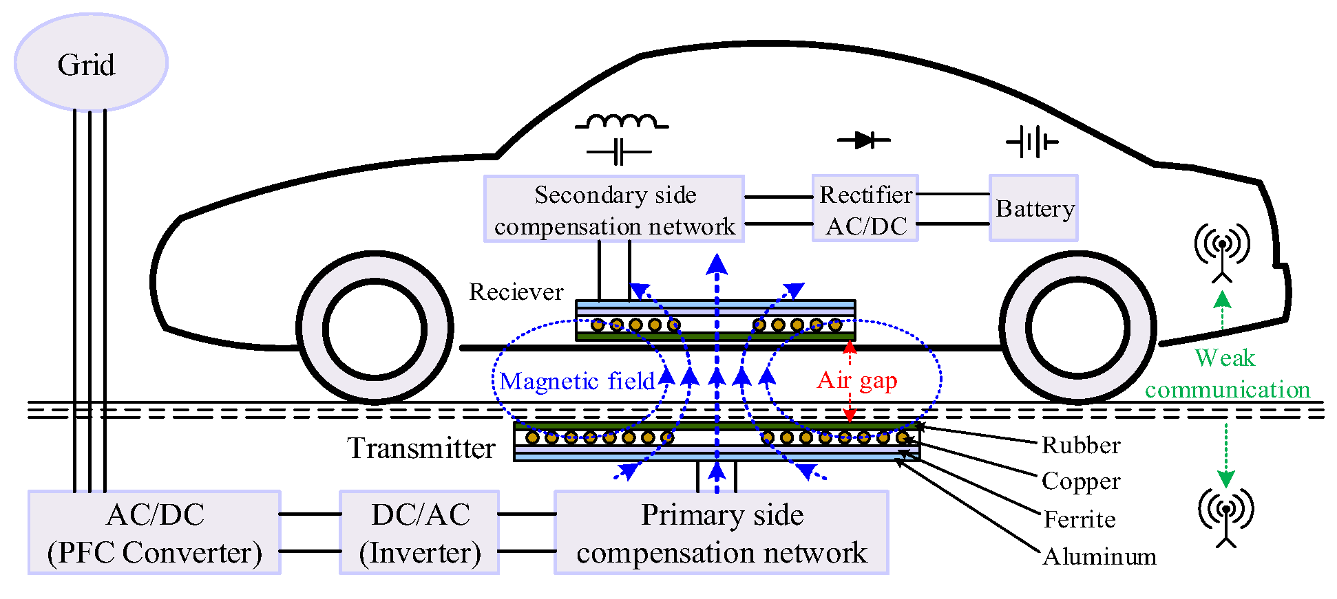
1. Introduction
2. Theoretical Analysis and Proposed Hybrid IPT System
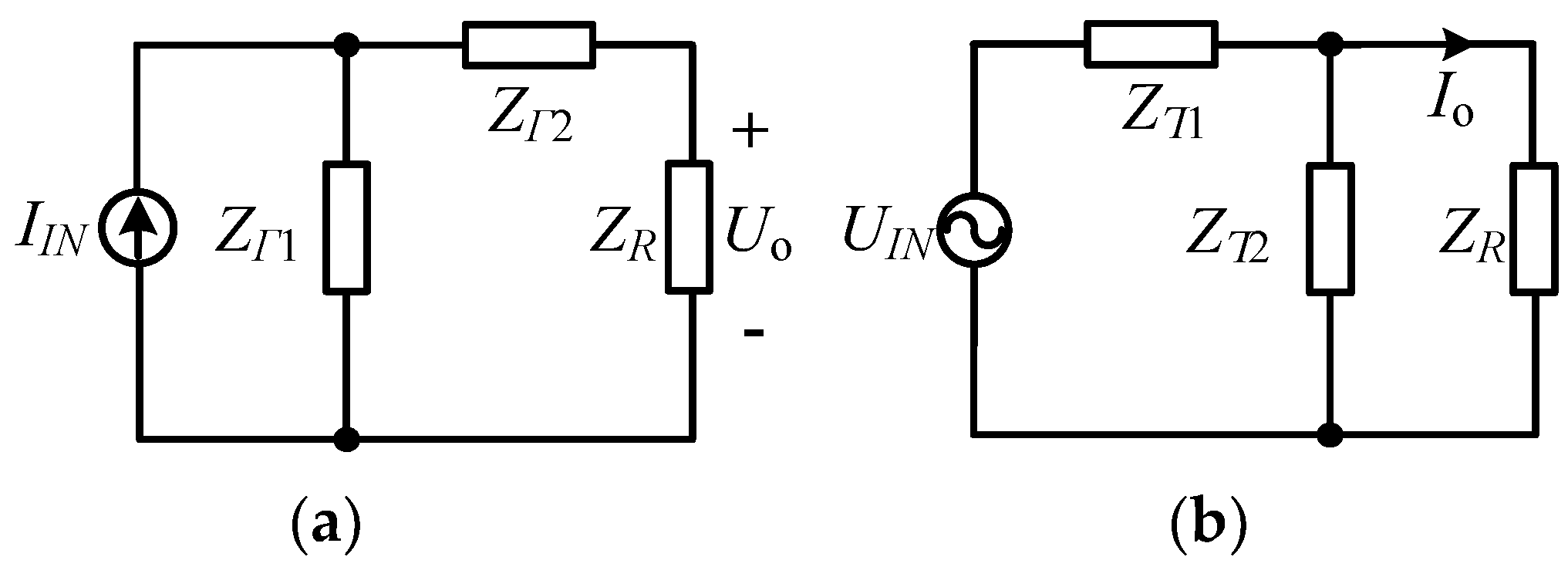
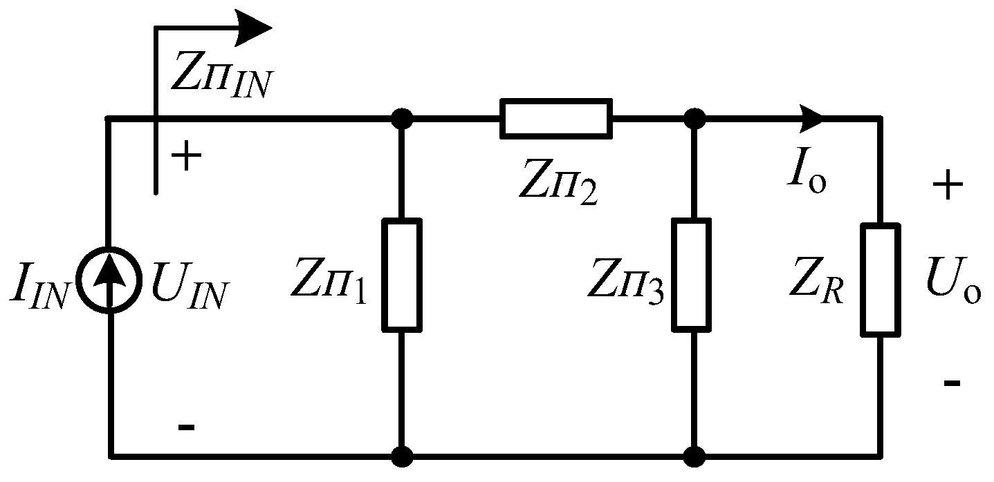
2.1. The Principle of Constant Voltage/Current Outputs of Second- and Third-Order Resonant Networks
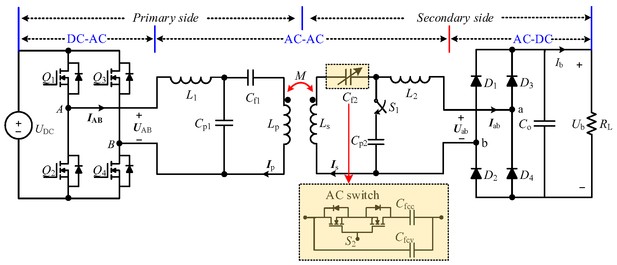
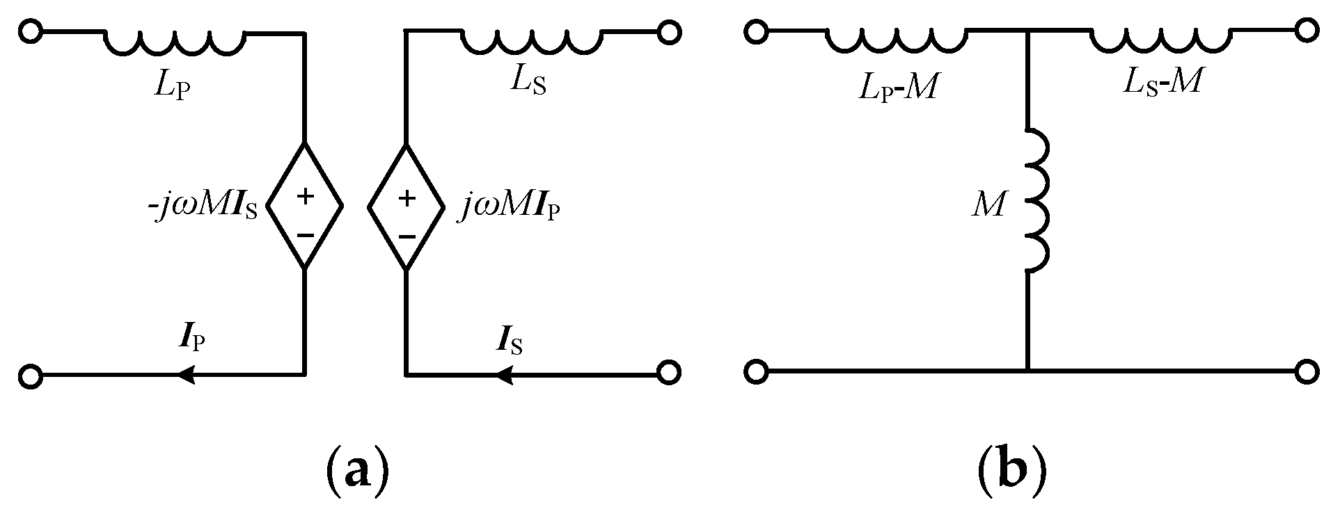
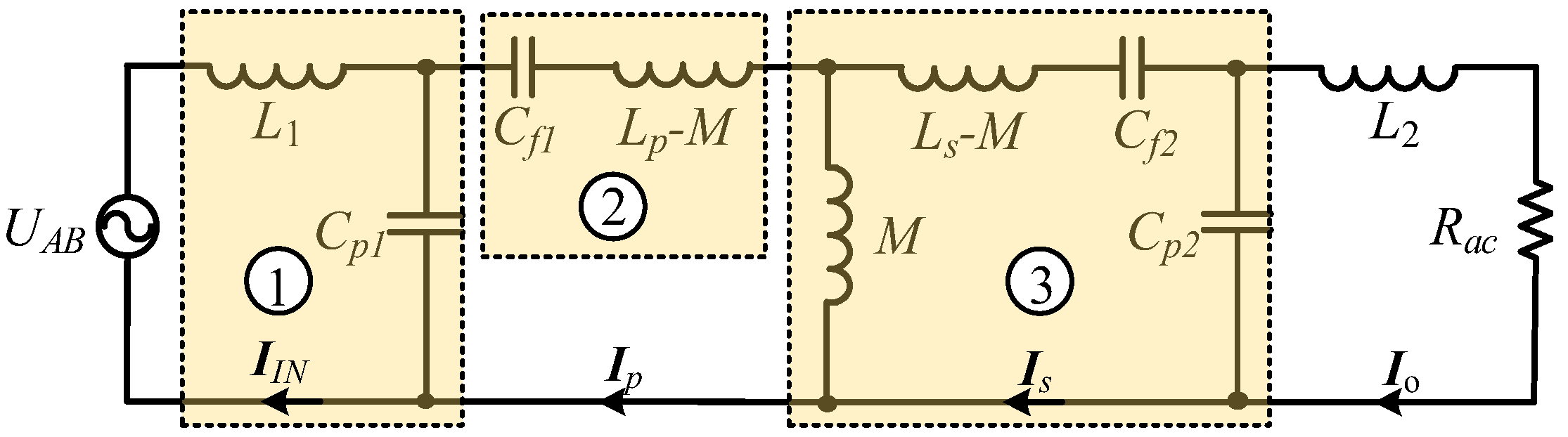
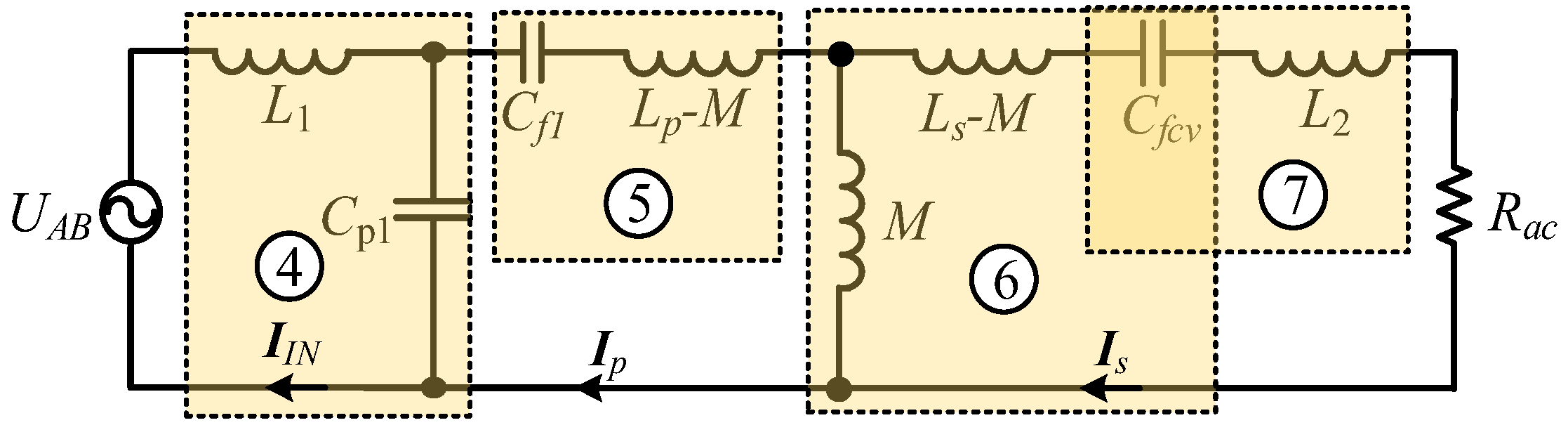
2.2. The Proposed Hybrid Compensation IPT System
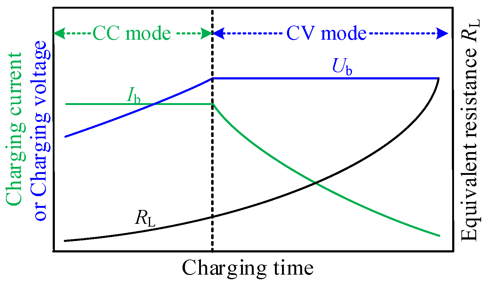
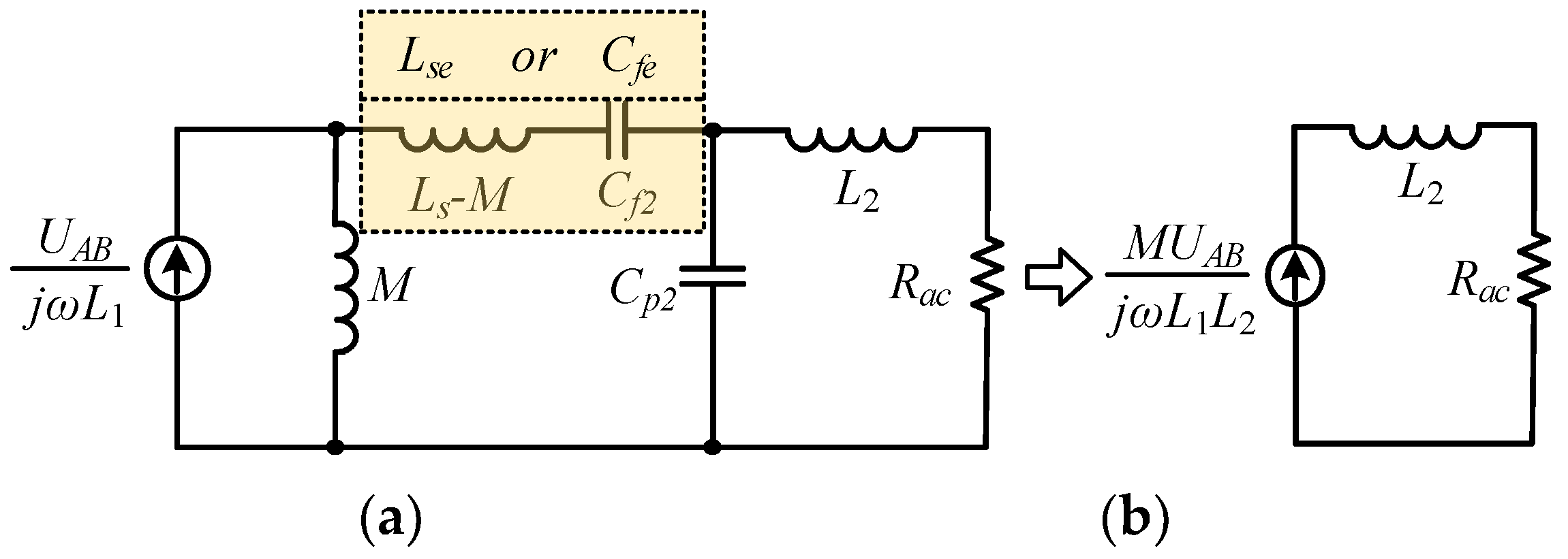
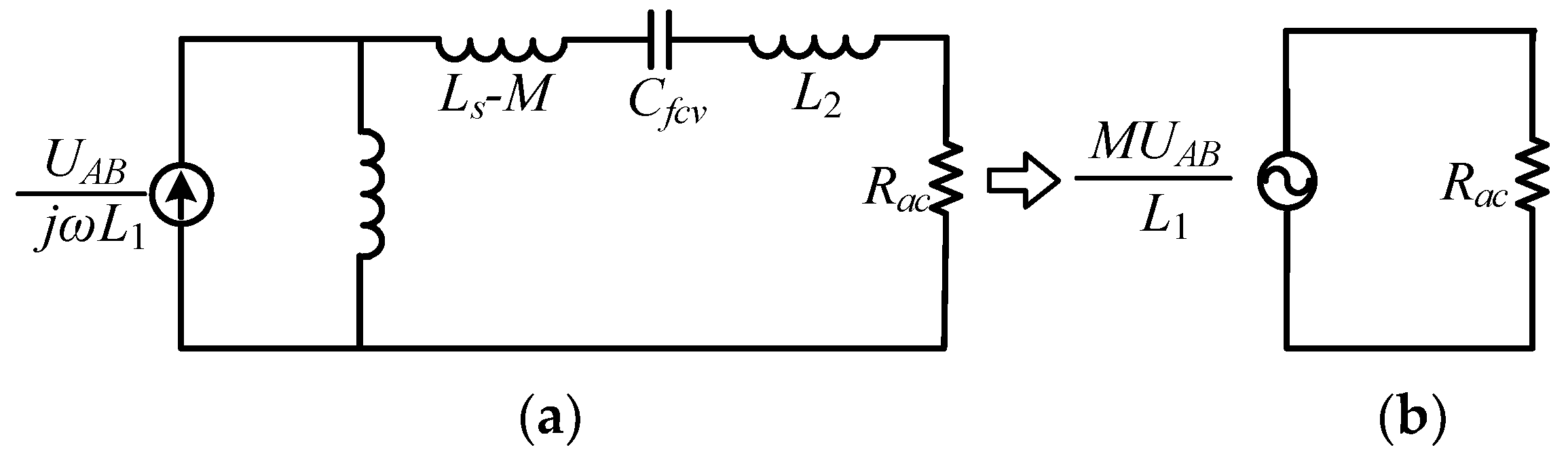
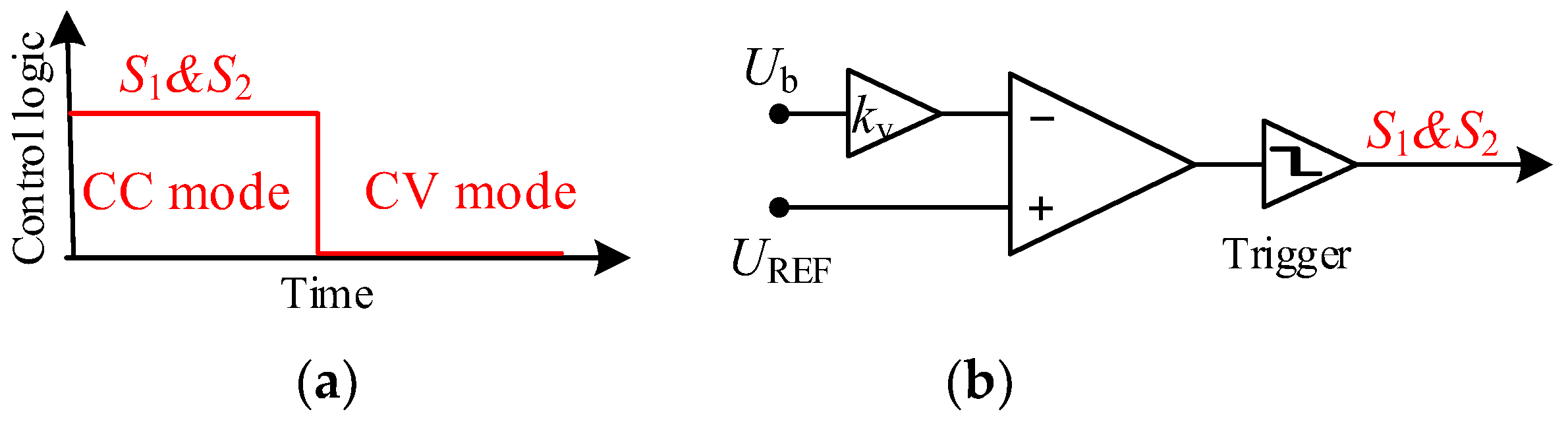
2.3. Analysis and Implementation of the CC Charging Mode with the ZPA Operation
2.4. Analysis and Implementation of the CC Charging Mode with the ZPA Operation
3. Design and Verification of Proposed Hybrid IPT Charger for CC/CV Modes
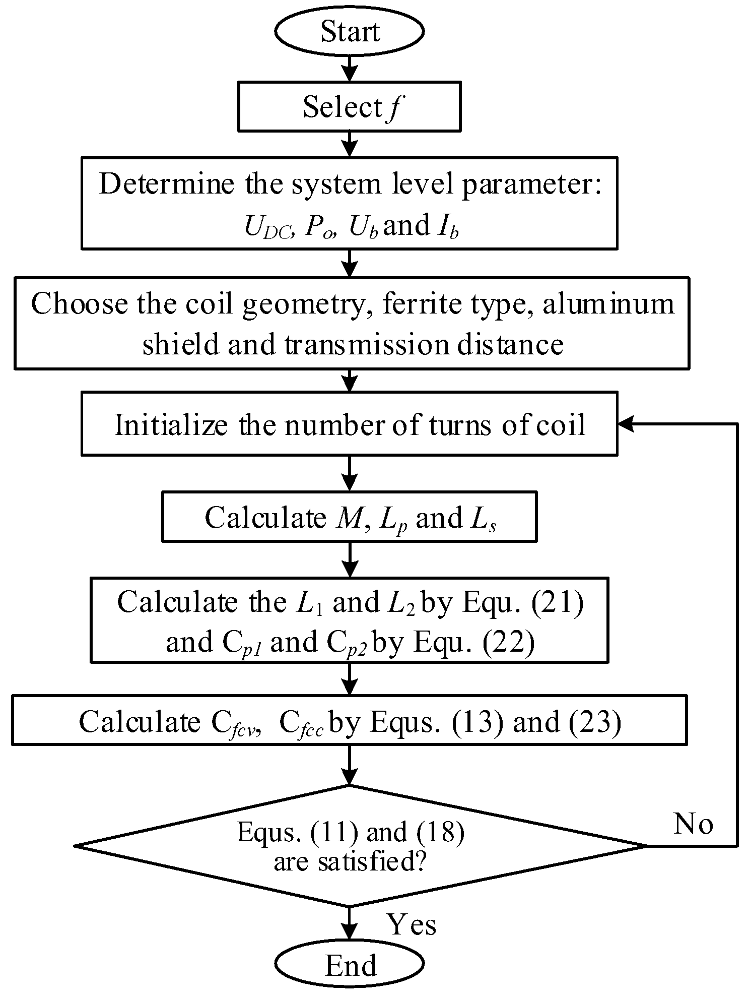
3.1. The Proposed Hybrid IPT Charger’s Parameter Design for CC/CV Modes
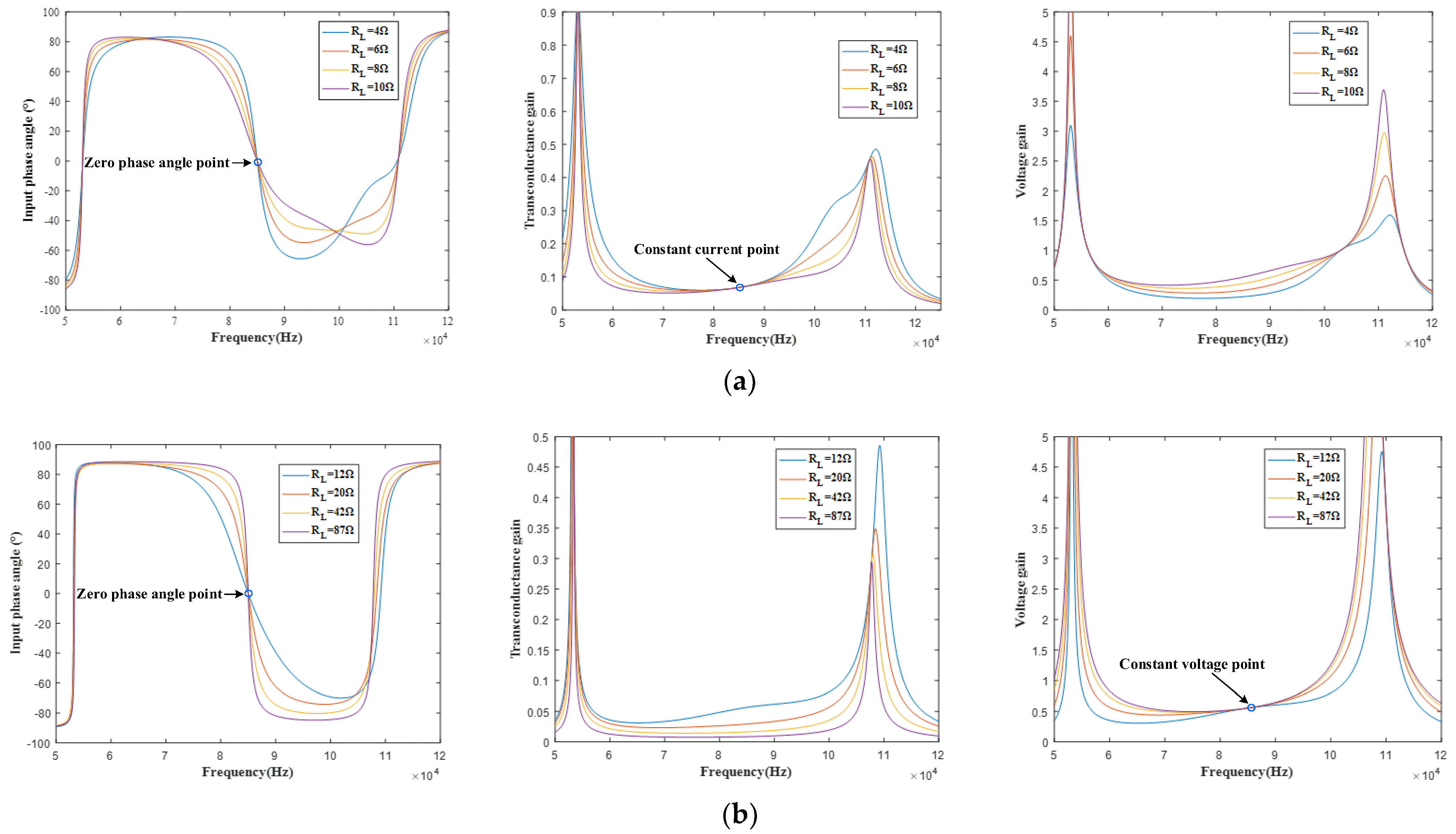
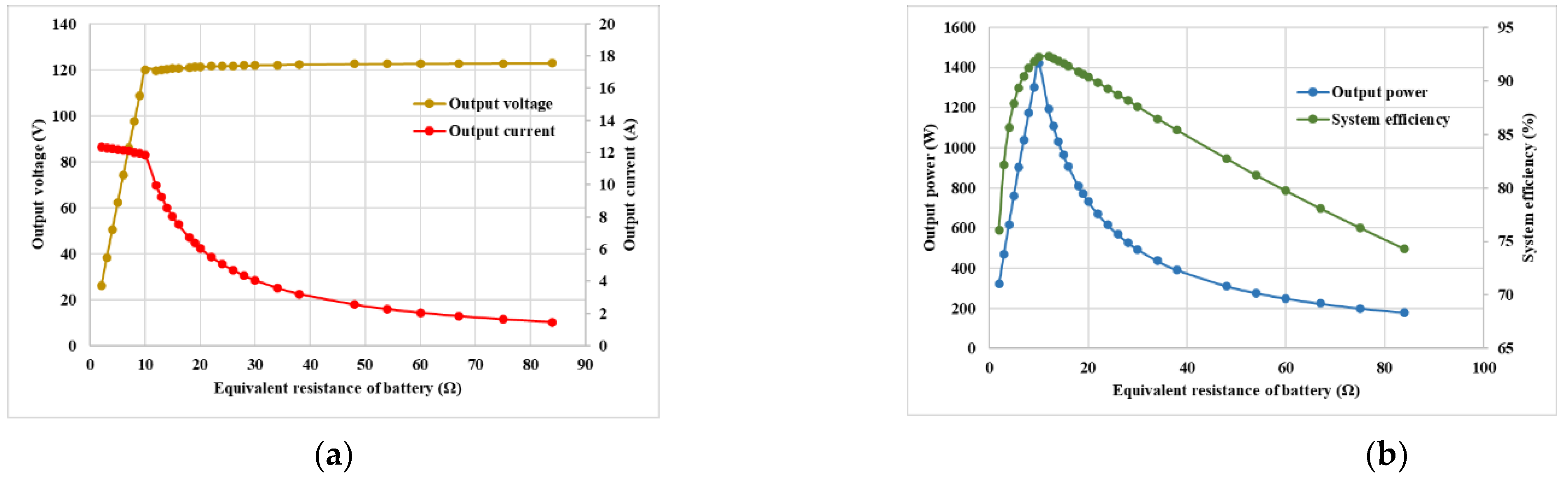
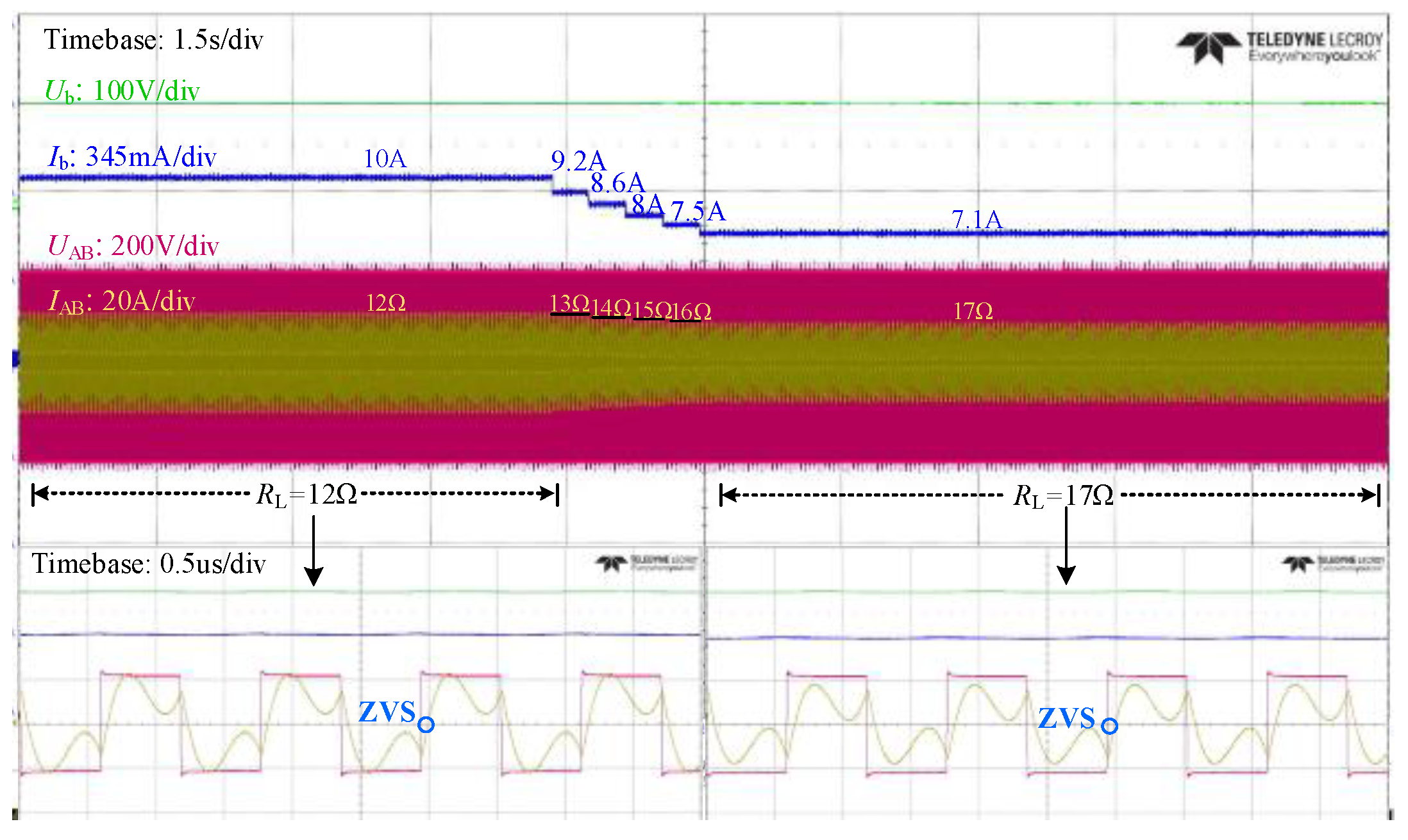
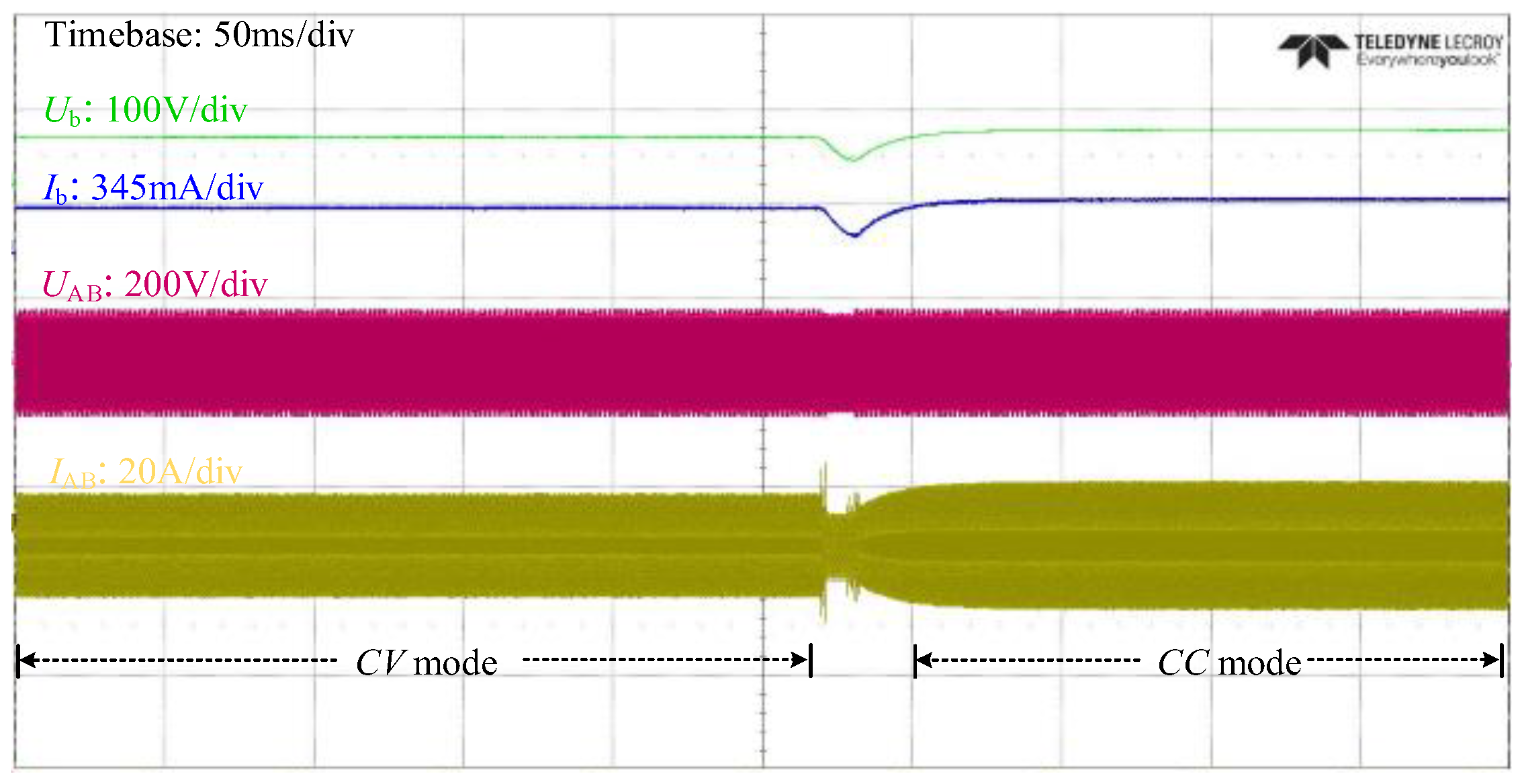
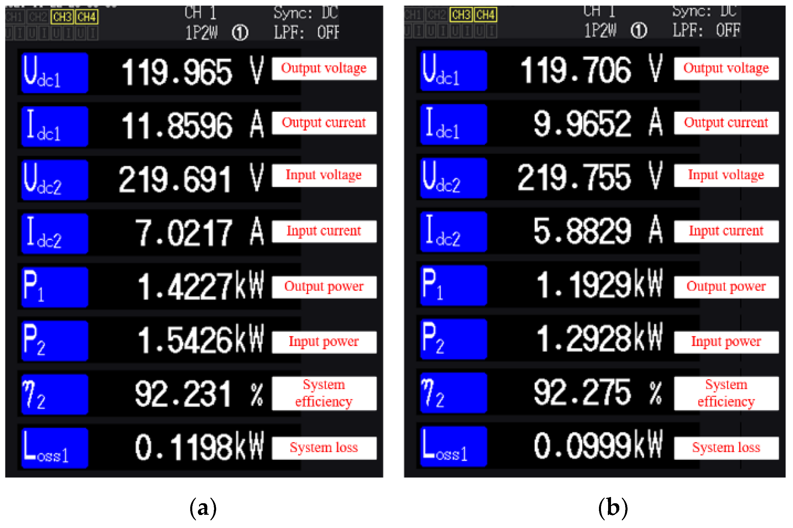
3.2. Verification of the Proposed IPT Charger for CC/CV Modes
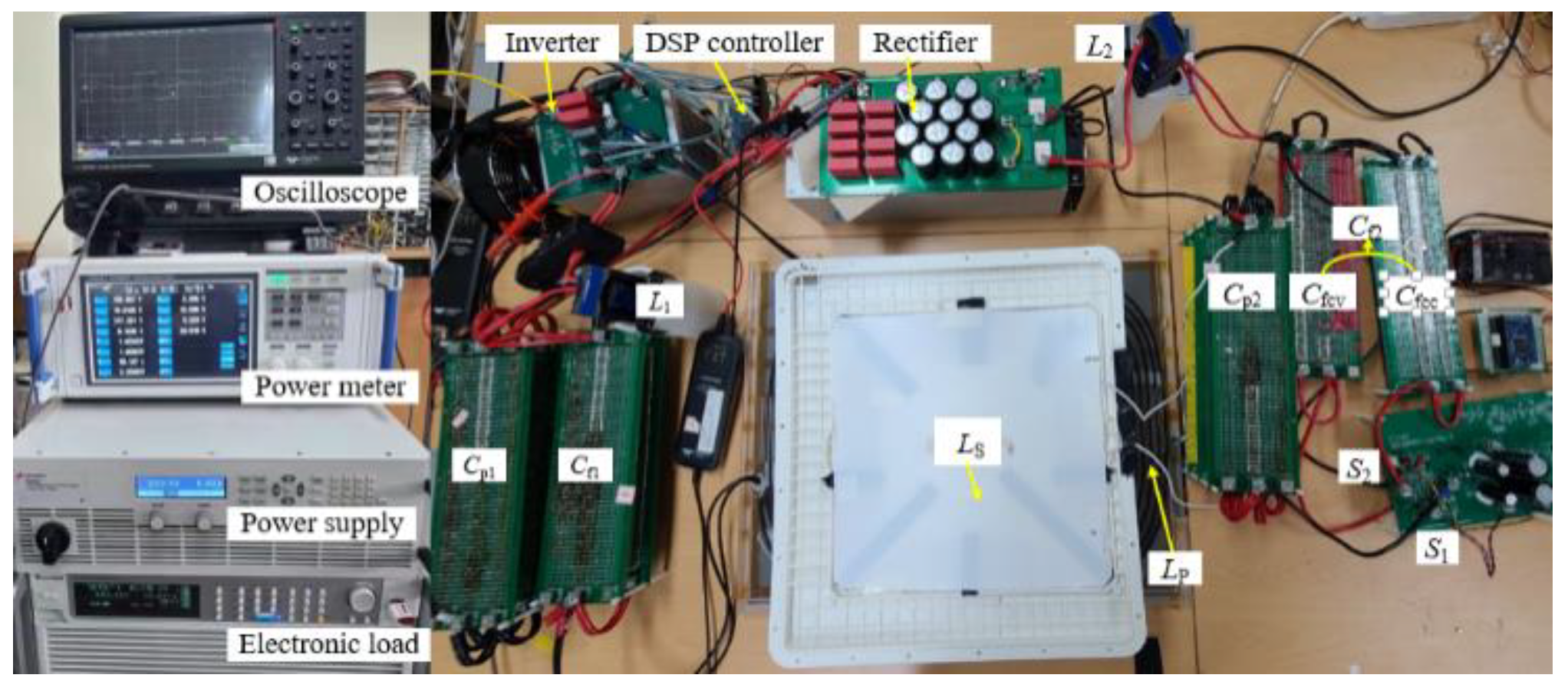
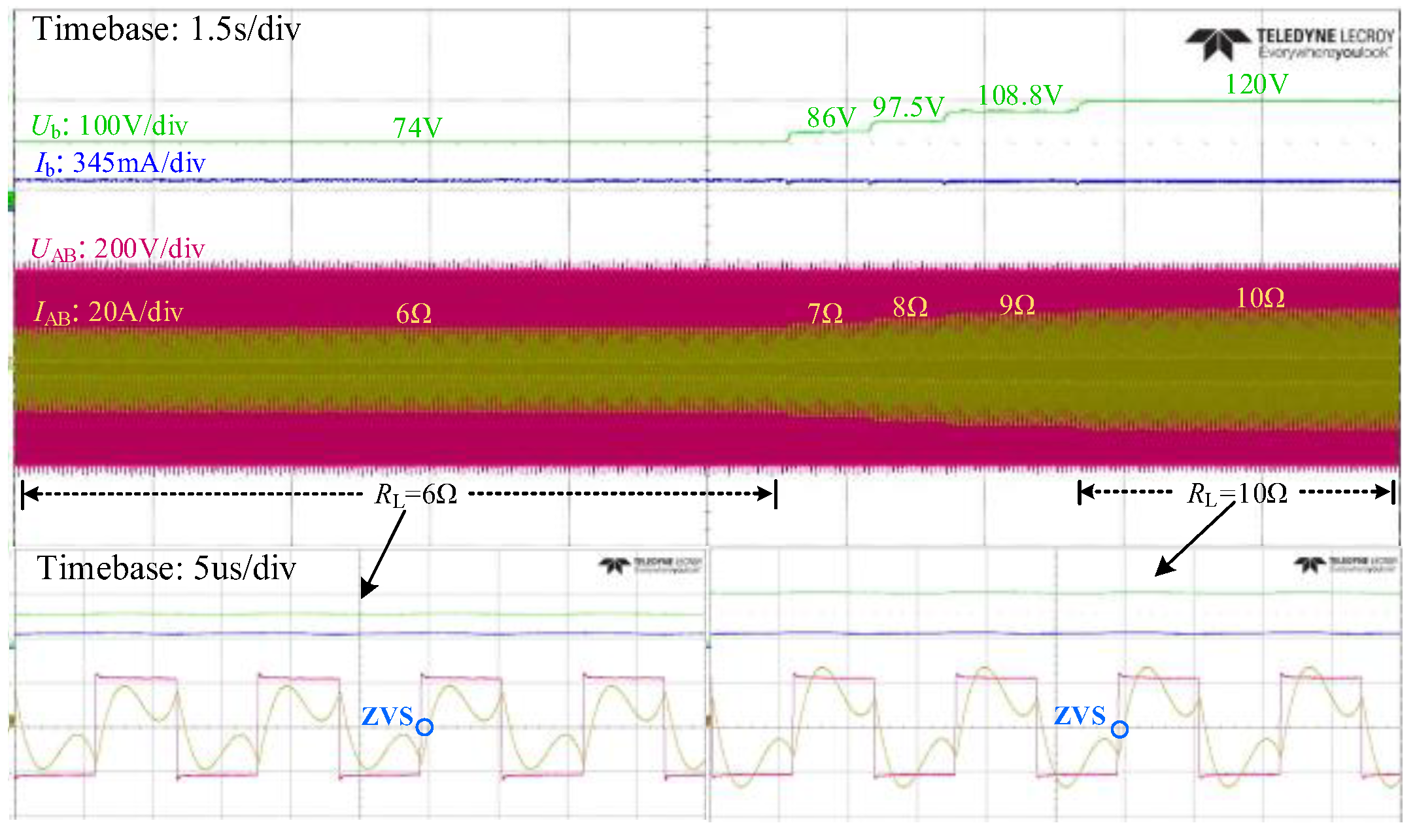
4. Experiment Verification
5. Conclusions
- (1)
- Only two ACSs had to be added on the secondary side. No additional compensation devices were needed and increases in the volume and weight were avoided. This satisfied the requirement of secondary side portability in the IPT system design.
- (2)
- The ZPA operation in the CC/CV modes can be easily realized, enhancing the proposed IPT charger’s efficiency.
- (3)
- Because the same driving signal was used to control the ACSs, the control strategy was relatively simple.
- (4)
- Secondary-side control was adopted. The configuration of the wireless communication links can be omitted to prevent the electromagnetic field from causing interference to the wireless communication links, which ensures the proposed charger’s robustness and reliability.
Author Contributions
Funding
Institutional Review Board Statement
Conflicts of Interest
References
- Hui, S.Y. Planar wireless charging technology for portable electronic products and Qi. Proc. IEEE 2013, 8, 1290–1301. [Google Scholar] [CrossRef]
- Covic, G.A.; Boys, J.T. Inductive power transfer. Proc. IEEE 2013, 101, 1276–1289. [Google Scholar] [CrossRef]
- Lee, W.Y.; Huh, J.; Choi, S.Y. Finite-width magnetic mirror models of mono and dual coils for wireless electric vehicles. IEEE Trans. Power Electron. 2013, 28, 1413–1428. [Google Scholar] [CrossRef]
- Choi, J.S.; Jeong, S.Y.; Choi, B.G.; Ryu, S.T.; Rim, C.T.; Kim, Y.S. Air-gap-insensitive IPT pad with ferromagnetic and conductive plates. IEEE Trans. Power Electron. 2019, 35, 7863–7872. [Google Scholar] [CrossRef]
- Tan, L.; Li, C.; Li, J.; Wang, R.; Huang, T.; Li, H.; Huang, X. Mesh-based accurate positioning strategy of EV wireless charging coil with detection coils. IEEE Trans. Ind. Electron. 2020, 17, 3176–3185. [Google Scholar] [CrossRef]
- Li, Y.; Hu, J.F.; Chen, F.B.; Liu, S.P.; Yan, Z.T.; He, Z.Y. A new-variable-coil-structure-based IPT system with load-independent constant output current or voltage for charging electric bicycle. IEEE Trans. Power Electron. 2018, 33, 8226–8230. [Google Scholar] [CrossRef]
- Liu, N.; Habetler, T.G. Design of a universal inductive charger for multiple electric vehicle models. IEEE Trans. Power Electron. 2015, 30, 6378–6390. [Google Scholar] [CrossRef]
- Zhao, Q.; Wang, A.; Liu, J.; Wang, X. The load estimation and power tracking integrated control strategy for dual-sides controlled LCC compensated wireless charging system. IEEE Access. 2019, 7, 75749–75761. [Google Scholar] [CrossRef]
- Wang, C.-S.; Covic, G.A.; Stielau, O.H. Power transfer capability and bifurcation phenomena of loosely coupled inductive power transfer systems. IEEE Trans. Ind. Electron. 2004, 51, 148–157. [Google Scholar] [CrossRef]
- Schormans, M.; Valente, V.; Demosthenous, A. Frequency splitting analysis and compensation method for inductive wireless powering of implantable biosensors. Sensors 2016, 16, 1229. [Google Scholar] [CrossRef]
- Vu, V.B.; Tran, D.H.; Choi, W. Implementation of the constant current and constant voltage charge of inductive power transfer systems with the double-sided LCC compensation topology for electric vehicle battery charge applications. IEEE Trans. Power Electron. 2018, 33, 7398–7410. [Google Scholar] [CrossRef]
- Berger, A.; Agostinelli, M.; Vesti, S.; Oliver, J.A.; Cobos, J.A.; Huemer, M. A wireless charging system applying phase-shift and amplitude control to maximize efficiency and extractable power. IEEE Trans. Power Electron. 2015, 30, 6338–6348. [Google Scholar] [CrossRef]
- Song, K.; Li, Z.; Jiang, J.; Zhu, C. Constant current/voltage charging operation for series-series and series-parallel compensated wireless power transfer systems employing primary-side controller. IEEE Trans. Power Electron. 2017, 33, 8065–8080. [Google Scholar] [CrossRef]
- Li, Z.; Zhu, C.; Jiang, J.; Song, K.; Wei, G. A 3-kW wireless power transfer system for sightseeing car supercapacitor charge. IEEE Trans. Power Electron. 2017, 32, 3301–3316. [Google Scholar] [CrossRef]
- Huang, Z.; Wong, S.-C.; Tse, C.K. Control design for optimizing efficiency in inductive power transfer systems. IEEE Trans. Power Electron. 2018, 33, 4523–4534. [Google Scholar] [CrossRef]
- Zhang, W.; Mi, C.C. Compensation topologies for high power wireless power transfer systems. IEEE Trans. Veh. Technol. 2016, 65, 4768–4778. [Google Scholar] [CrossRef]
- Zhang, W.; Wong, S.C.; Tse, C.K.; Chen, Q. Design for efficiency optimization and voltage controllability of series–series compensated inductive power transfer systems. IEEE Trans. Power Electron. 2014, 29, 191–200. [Google Scholar] [CrossRef]
- Li, S.Q.; Mi, C.C. Wireless power transfer for electric vehicle applications. IEEE J. Emerg. Sel. Top. Power Electron. 2015, 3, 4–17. [Google Scholar]
- Hwang, S.H.; Chen, Y.F.; Zhang, H.L.; Lee, K.Y.; Kim, D.-H. Reconfigurable hybrid resonant topology for constant current/voltage wireless power transfer of electric vehicles. Electronics 2020, 9, 1323. [Google Scholar] [CrossRef]
- Wang, C.W.; Stielau, O.H.; Covic, G.A. Design considerations for a contactless electric vehicle battery. IEEE Trans. Power Electron. 2005, 52, 1308–1314. [Google Scholar] [CrossRef]
- Auvigne, C.; Germano, P.; Ladas, D.; Perriard, Y. A dual-topology ICPT applied to an electric vehicle battery charger. In Proceedings of the International Conference on Electrical Machines, Marseille, France, 2–5 September 2012; pp. 2287–2292. [Google Scholar]
- Qu, X.; Han, H.; Wong, S.C.; Tse, C.K.; Chen, W. Hybrid WPT topologies with constant current or constant voltage output for battery charging applications. IEEE Trans. Power Electron. 2015, 30, 6329–6337. [Google Scholar] [CrossRef]
- Li, J.G.; Zhang, X.Z.; Tong, X.Q. Research and design of misalignment-tolerant LCC-LCC compensated IPT cystem with constant-current and constant-voltage output. IEEE Trans. Power Electron. 2022, 38, 1301–1313. [Google Scholar] [CrossRef]
- Wang, Y.; Wang, H.; Liang, T.; Zhang, X.; Xu, D.; Cai, L. Analysis and design of an LCC/S compensated resonant converter for inductively coupled power transfer. In Proceedings of the 2022 IEEE Transportation Electrification Conference and Expo, Asia-Pacific, Harbin, China, 7–10 August 2017; pp. 1–5. [Google Scholar]
- Chen, Y.; Kou, Z.; Zhang, Y.; He, Z.; Mai, R.K.; Cao, G. Hybrid topology with configurable charge current and charge voltage output-based WP T charger for massive electric bicycles. IEEE J. Emerg. Sel. Topics Power Electron. 2018, 6, 1581–1594. [Google Scholar] [CrossRef]
- Zhang, H.L.; Chen, Y.F.; Park, S.J.; Kim, D.-H. A switching hybrid LCC-S compensation topology for constant current/voltage EV wireless charging. IEEE Access. 2019, 7, 133924–133935. [Google Scholar]
- Zhang, H.L.; Chen, Y.F.; Park, S.J.; Kim, D.-H. Hybrid compensation topology with single switch for battery charging of inductive power transfer systems. IEEE Access. 2019, 7, 171095–171104. [Google Scholar] [CrossRef]
- Cai, C.S.; Wang, J.; Fang, Z.; Zhang, P.; Hu, M.; Zhang, J.; Li, L.; Lin, Z. Design and optimization of load-independent magnetic resonant wireless charging system for electric vehicles. IEEE Access. 2018, 6, 17264–17274. [Google Scholar] [CrossRef]
- Zhang, H.L.; Chen, Y.F.; Jo, C.H.; Park, S.J.; Kim, D.H. DC-link and switched capacitor control for varying coupling conditions in inductive power transfer system for unmanned aerial vehicles. IEEE Trans. Power Electron. 2020, 36, 5108–5120. [Google Scholar] [CrossRef]
- Zhang, W.; Song, J.; Xu, C.; Lin, L.; Ren, H.; Gao, Y. Implementation of constant current or constant voltage output based on switching circuit for battery charging applications. In Proceedings of the 2021 IEEE 5th Conference on Energy Internet and Energy System Integration (EI2), Taiyuan, China, 22–24 October 2021; pp. 3900–3904. [Google Scholar]
- Li, G.Y.; Kim, D.-H. A wireless power transfer charger with hybrid compensation topology for constant current/voltage onboard charging. Appl. Sci. 2021, 11, 7569. [Google Scholar] [CrossRef]
- Chen, Y.; Li, M.; Yang, B.; Chen, S.; Li, Q.; He, Z.; Mai, R. Variable-parameter T-circuit-based IPT system charging battery with constant current or constant voltage output. IEEE Trans. Power Electron. 2019, 35, 1672–1684. [Google Scholar] [CrossRef]
- Li, S.Q.; Li, W.H.; Deng, J.J.; Nguyen, T.D.; Mi, C.C. A double-sided LCC compensation network and its tuning method for wireless power transfer. IEEE Trans. Veh. Technol. 2015, 64, 2261–2273. [Google Scholar] [CrossRef]
- Erickson, R.W.; Maksimovic, D. Fundamentals of Power Electronics, 2nd ed.; Kluwer: Norwell, MA, USA, 2001. [Google Scholar]
- Mai, R.K.; Chen, Y.; Li, Y.; Zhang, Y.Y.; Cao, G.Z.; He, Z.Y. Inductive power transfer for massive electric bicycles charging based on hybrid topology switching with a single inverter. IEEE Trans. Power Electron. 2017, 32, 5897–5906. [Google Scholar] [CrossRef]
- Wang, W.; Deng, J.J.; Chen, D.L.; Wang, Z.P.; Wang, S. A novel design method of LCC-S compensated inductive power transfer system combining constant current and constant voltage mode via frequency switching. IEEE Access. 2021, 9, 117244–117256. [Google Scholar] [CrossRef]


| Symbols | Value | Symbols | Value |
|---|---|---|---|
| U IN | 220 V | L1 | 15.25 µH |
| f | 85 kHz | L2 | 15.15 µH |
| Cp1 | 229.83 nF | Cfcc | 76.025 nF |
| Cp2 | 229.79 nF | Cfcv | 63.045 nF |
| Cf1 | 145.67 nF |
| Symbols | Value | Symbols | Value |
|---|---|---|---|
| k | 0.206 | M | 8.45 µH |
| Lp | 41.63 µH | RLp | 36.64 mΩ |
| Ls | 40.41 µH | RLs | 41.98 mΩ |
| Proposed in | Ref. [6] | Ref. [14] | Ref. [19] | Ref. [25] | Ref. [26] | Ref. [27] | Ref. [35] | Ref. [36] | This Work |
|---|---|---|---|---|---|---|---|---|---|
| Inductors | 1 | 0 | 1 | 2 | 1 | 1 | 1 | 1 | 2 |
| Capacitors | 4 | 2 | 4 | 5 | 5 | 3 | 3 | 3 | 4 |
| ACSs | 2 | 0 | 2 | 2 | 2 | 1 | 2 | 0 | 2 |
| Number of DC-DC converters | 0 | 1 | 0 | 0 | 0 | 0 | 0 | 0 | 0 |
| Location of ACSs | Receiver | No | Transmitter | Receiver | Both sides | Transmitter | Receiver | No | Receiver |
| Wireless communication | Yes | Yes | Yes | No | Yes | Yes | No | Yes | No |
| Design freedom in CC/CV modes | No/No | No/No | No/Yes | Yes/Yes | Yes/Yes | No/Yes | No/Yes | Yes/Yes | Yes/Yes |
| Control frequency | Fixed | Fixed | Fixed | Fixed | Fixed | Changed | Fixed | Changed | Fixed |
| Max. power | 0.96 kW | 3.25 kW | 3 kW | 0.22 kW | 2.5 kW | 0.2 kW | 2 kW | 3.5 kW | 1.4 kW |
| Peak efficiency | 87.3% | 88.05% | 92.58% | 91.89% | 89.28% | 87% | 92.81% | 97.3% | 92.3% |
Publisher’s Note: MDPI stays neutral with regard to jurisdictional claims in published maps and institutional affiliations. |
© 2022 by the authors. Licensee MDPI, Basel, Switzerland. This article is an open access article distributed under the terms and conditions of the Creative Commons Attribution (CC BY) license (https://creativecommons.org/licenses/by/4.0/).
Share and Cite
Li, G.; Jo, C.-H.; Shin, C.-S.; Jo, S.; Kim, D.-H. A Load-Independent Current/Voltage IPT Charger with Secondary Side-Controlled Hybrid-Compensated Topology for Electric Vehicles. Appl. Sci. 2022, 12, 10899. https://doi.org/10.3390/app122110899
Li G, Jo C-H, Shin C-S, Jo S, Kim D-H. A Load-Independent Current/Voltage IPT Charger with Secondary Side-Controlled Hybrid-Compensated Topology for Electric Vehicles. Applied Sciences. 2022; 12(21):10899. https://doi.org/10.3390/app122110899
Chicago/Turabian StyleLi, Guangyao, Cheol-Hee Jo, Chang-Su Shin, Seungjin Jo, and Dong-Hee Kim. 2022. "A Load-Independent Current/Voltage IPT Charger with Secondary Side-Controlled Hybrid-Compensated Topology for Electric Vehicles" Applied Sciences 12, no. 21: 10899. https://doi.org/10.3390/app122110899
APA StyleLi, G., Jo, C.-H., Shin, C.-S., Jo, S., & Kim, D.-H. (2022). A Load-Independent Current/Voltage IPT Charger with Secondary Side-Controlled Hybrid-Compensated Topology for Electric Vehicles. Applied Sciences, 12(21), 10899. https://doi.org/10.3390/app122110899