Review

A Review of Cell Operation Algorithm for 3D NAND Flash Memory

by
Jong Kyung Park
and
Sarah Eunkyung Kim
*
Department of Semiconductor Engineering, Seoul National University of Science and Technology, Gongneung-ro 232, Nowon-gu, Seoul 01811, Korea
*
Author to whom correspondence should be addressed.
Appl. Sci. 2022, 12(21), 10697; https://doi.org/10.3390/app122110697
Submission received: 29 September 2022 / Revised: 16 October 2022 / Accepted: 19 October 2022 / Published: 22 October 2022

Abstract

:
The size of the memory market is expected to continue to expand due to the digital transformation triggered by the fourth industrial revolution. Among various types of memory, NAND flash memory has established itself as a major data storage medium based on excellent cell characteristics and manufacturability; as such, the demand for increasing the bit density and the performance has been rapidly increasing. In this paper, we will review the device operation algorithm and techniques to improve the cell characteristics and reliability in terms of optimization of individual program, read and erase operation, and system level performance.

1. Introduction

As 2D NAND faces physical limitations such as an increase in cell-to-cell interference and a decrease in the number of electrons per unit cell [1], NAND business has embraced a dramatic transition to 3D NAND to achieve the cost per bit scaling trend [2]. Three-dimensional NAND memory has a word line (WL) stacked structure in which the gate electrode and the insulating film are alternately stacked with a hole penetrating from the top layer to the bottom layer via a single etching process [3], which dramatically lowers the process cost while significantly increasing the cell dimensions compared to 2D NAND, and thereby greatly improve the performance and reliability characteristics [4]. However, over the last few years in 3D NAND manufacturing, as the physical dimensions of the unit cell have decreased to continuously improve the bit density, cell-to-cell interference and retention characteristics have begun spontaneously to deteriorate [5]. On the other hand, not only the bit density but also the chip performance requirements, such as the programming throughput, have been continuously increasing in the market [6], as shown in Figure 1. Therefore, the current 3D NAND industry is struggling with a double hardship in which it is necessary to improve various cell characteristics caused by small unit cell size and also improve the device performance. Thus far, one direction to address the above technology challenges is the development of new process integration and materials, and many review papers have reported on this [7,8,9]. However, there has been few reviews from the perspective of device operation techniques and algorithms, although many studies are being conducted.
In this paper, we will review a device operation algorithms and techniques to improve the cell characteristics and reliability in terms of optimization of individual program, read and erase operation, and system level performance. This paper is composed of three sections of Program, Read, and Erase operations in Section 2, Section 3 and Section 4, respectively. Each section will be subdivided into several areas in terms of the major research directions and briefly describe the background of individual algorithms, ideas to be improved, and some technical limitations.

2. Program Algorithm

The major motivations for developing program operation can be roughly divided into three categories. The first is to improve the program disturbance characteristics during program operation; the second is to reduce the programming time to improve the performance of the NAND chip; the third is to improve device reliability caused by 3D NAND geometry and process integration.

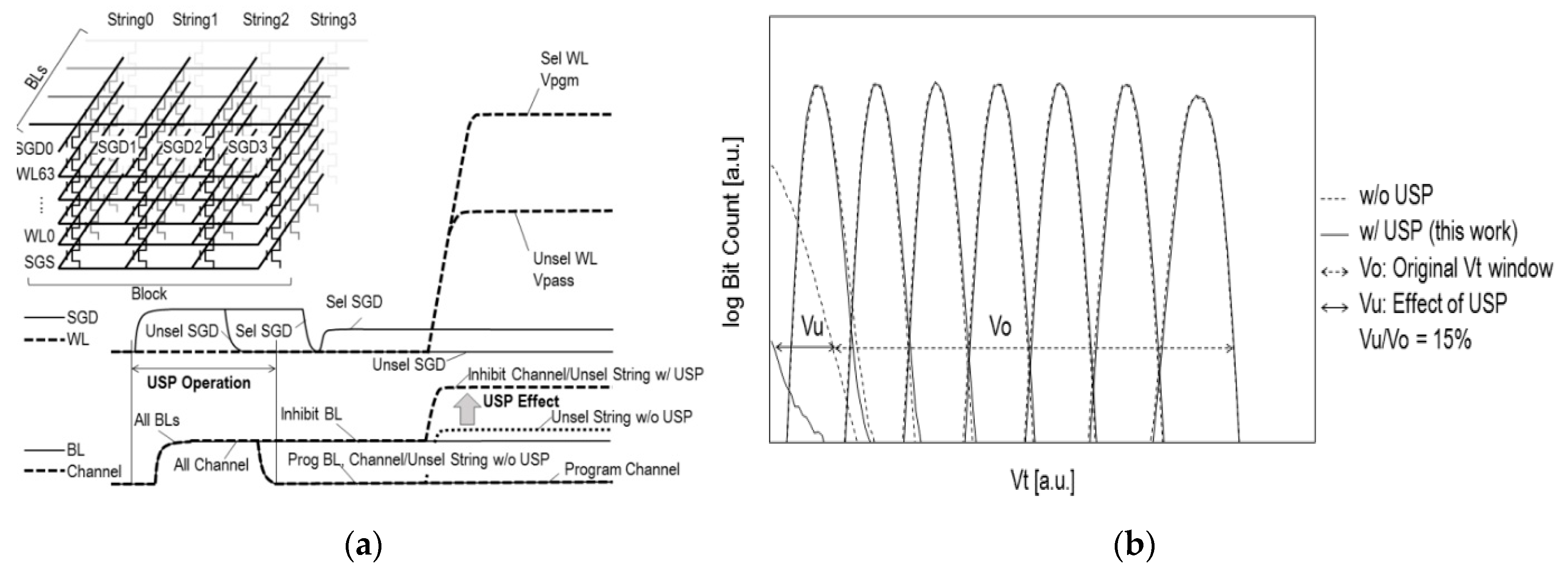
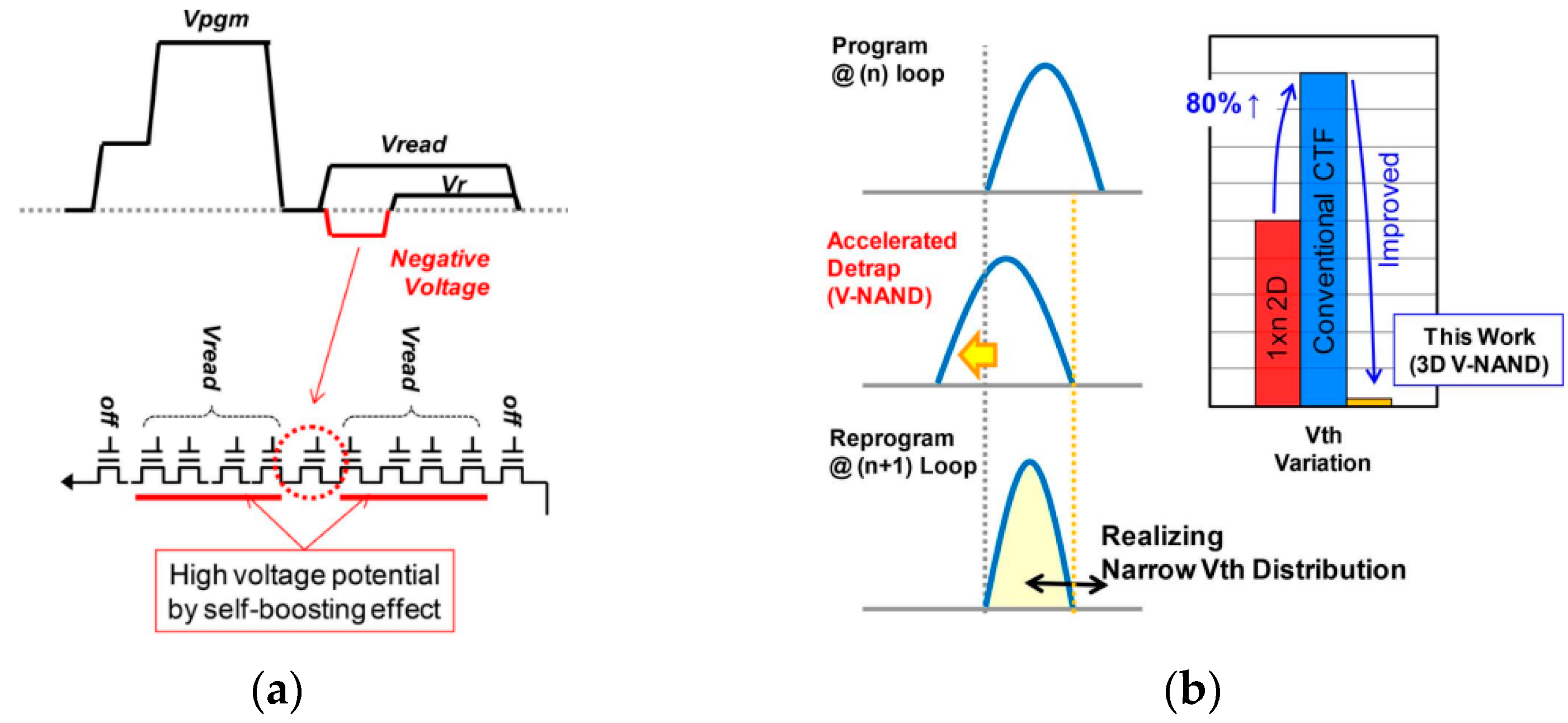
2.1. Improvement of the Program Disturb

Compared to 2D NAND, there is a possibility that the program disturbance characteristics in 3D NAND are severely deteriorated due to the following reasons. First, because there are multiple strings in one block, new program disturbance stress modes, such as Y-mode and XY-mode, are added in conjunction with X-mode disturbances existing in 2D NAND [12]. In particular, since the number of slits for block-to-block separations is reduced to increase the chip density [11], the number of strings is expected to increase continuously; thereby, Y-mode program stress will be the main cause further diminishing the memory window. Second, since 3D NAND uses poly-silicon as channel material, the on/off characteristic of the select transistor is much worse than that of 2D NAND, and the off-state leakage current flows through the select gate in boosting mode, which weaken the program disturbance [13]. Third, since it is difficult to remove electrons in the poly-silicon channel during the pre-charge operation due to the grain boundary trap [14,15], achieving high channel potential in boosting mode is very challenging. Fourth, when large channel potential difference between adjacent WLs is applied in the end of programming loop [16], the electron/hole pair generated via the trap-assisted band-to-band tunneling (BTBT) mechanism reduces the channel boosting potential [17,18]. Fifth, due to the floating body characteristics of 3D NAND, a negative down-coupling phenomenon occurs during the falling of the verify pulse of the selected and the unselected WLs [19], aggravating the deterioration of the hot carrier injection (HCI) program disturb [20]. In this respect, various enhancement algorithms to improve the obstacles of the above program disturb will be described.
Shim et al. proposed a few approaches to suppress the program disturbance: keeping higher Vt level of top select transistor and adopting the negative top select transistor bias during program operation [12]. In the Y-mode program disturbance, unselected strings hanging on the same BL in the program cell should be inhibited with the same BL bias 0 V. Therefore, both forming a high Vt level of the top select transistor and applying the negative bias in top select transistor during program operation can present better cut-off characteristics of select transistors. However, if too high a negative voltage is applied, gate-induced drain leakage (GIDL) current is rapidly generated at the junction overlap region underneath the select transistor, which could make boosting level lower.
To reduce the increasing Y-mode program stress, Yamashita et al. proposed an improved pre-charging method [21], as shown in Figure 2. A block has several upper select transistors, while WLs and lower select transistors are shared within a block. The sharing of WLs allows the memory area to be reduced; however, the unselected strings are also disturbed, since the program voltage is applied through the shared WLs. To decrease program disturbance of an unselected string, a very high bit line (BL) bias is applied to the unselected string before the program operation, enhancing the initializing efficiency of the channel potentials. However, for this operation, a high BL bias must be transmitted to the channels of unselected strings, so there is a side effect of an increase in programming time. Therefore, this method is not used at the beginning of ISPP operation, but only during the last program pulse loop, when channel boosting is insufficient to minimize program disturbance degradation.
On the other hand, to further improve the program disturbances caused by electrons trapped at the grain boundary of the poly silicon channel, Zhang et al. proposed a new pre-charge method [22]. Due to the limited carrier mobility of poly-Si channel, the conventional BL pre-charge scheme is not strong enough to initialize the channel potential of an unselected string [23]. To enhance the pre-charging efficiency, the BL pre-charging voltage has to be increased, and thereby, the pre-turn on voltage of the upper select transistor is also increased [21]. In this paper, however, the pre-turn on the voltage of the upper select transistor is applied even as ground. This scheme demonstrates that program disturb can be improved by directly supplying holes into the channel by implementing an operation method similar to the GIDL current formation of the erase operation [3]. However, to implement this method, a high voltage gap of 4 V or higher must be applied between the BL and the select transistor because the GIDL current must be sufficiently generated [24]. In this case, it will be necessary to develop a page buffer circuit to drive a high BL bias and additional revision to compensate for the increased programming time due to a longer GIDL generation time.
In addition, to reduce the trap-assisted BTBT current generated by grain boundary trap, a method of arranging a dummy WL bias between the select transistor and the main cell during program operation was proposed [12,25]. By gradually adjusting their pass voltage during program operation, program disturbances caused by HCI were also reduced. Meanwhile, in respect to optimization of dummy WL operation during program, W.-C. Chen et al. proposed a two-step pulse method [26] in which a low pre-voltage is first applied in the BL pre-charge period and then a relatively high dummy WL bias is applied in the program pulse period, rather than simply applying a same bias to the dummy WL at once. This technique demonstrates that it is possible to control HCI program disturbance from the dummy WL, by reducing the transverse electric field between the dummy WL and the edge main WL.
W.-L. Lin et al. proposed a method of minimizing negative down-coupling by holding the pass voltage of unselected WLs after the verify operation [27]. Their programming algorithm consists of a sequence of a program operation followed by a verify operation to check if the target threshold voltage is reached; this process is repeated with increasing program voltages until all cells on the page have reached the target threshold voltage [28]. In 3D-NAND architectures, since the conductive path is not formed in the string except for BL and source line (SL), the channel potential can capacitively couple with WLs and drop to negative voltages when WL voltage falls during the verify operation [19]. In this approach, holding a pass voltage of unselected WLs without lowering it to the ground after the verify operation is finished is suggested. However, this method can lower the boosting efficiency during subsequent program operation, and so may cause soft programming disturb. Another recommendation is to softly turn on the WLn-1/n-2 cells before the program operation. This shares the channel potential of the down-coupled cell region with other regions so that subsequent high lateral electric fields are not applied, relieving the HCI disturbance; however, this pre-turn on condition consumes extra time, degrading program performance.
Apart from the above circuit-level or chip-level hardware-based approaches, some software-based approaches can provide one part of the solution to mitigate the program disturbance. Y.-M. Chang et al. proposed a programming method by dividing one physical block into two logical sub-blocks (referred to as reliable blocks) [29]. The selected pages to form a reliable block are not adjacent with each other. Thus, programming each page in a reliable block with interlaced mapping causes minimal disturbance to other pages in the same reliable block.

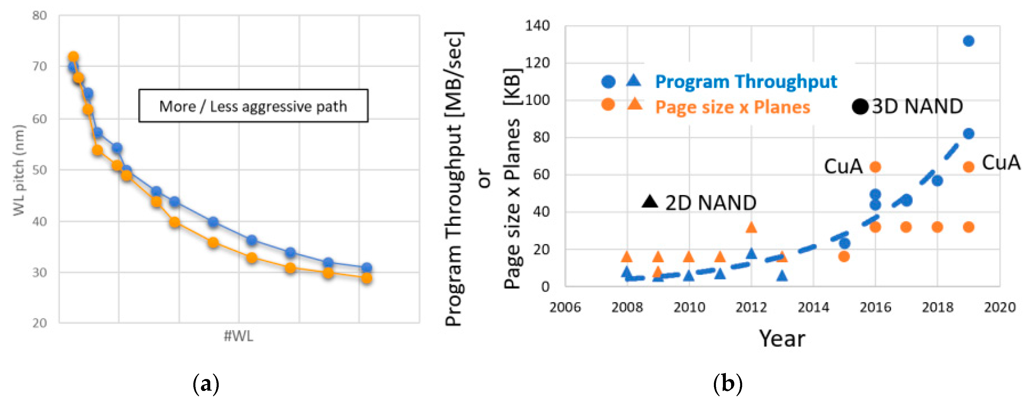
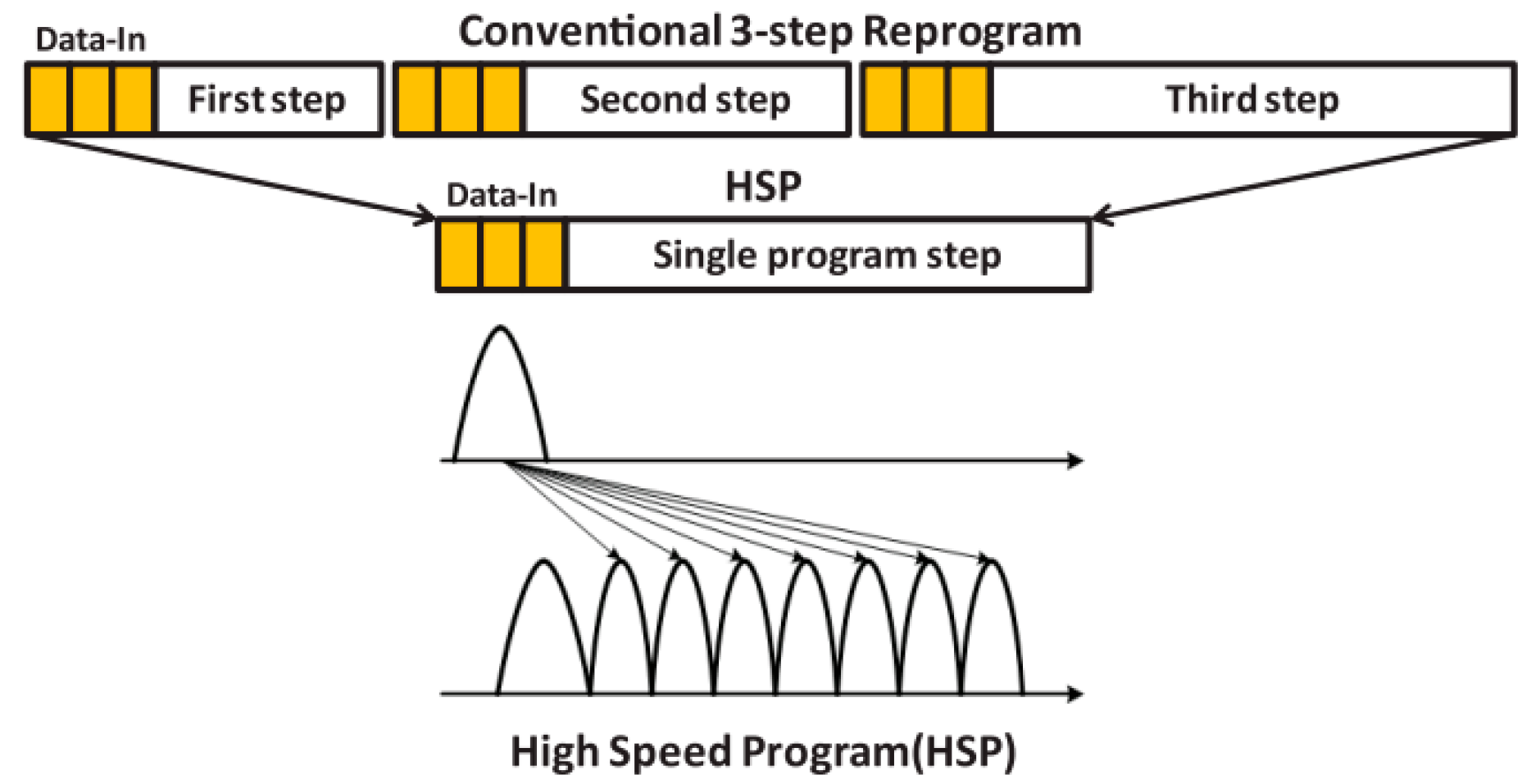
2.2. Improvement of Program Performance

Most major 3D NAND memory manufacturers, such as Samsung, SK Hynix, and Micron, began to produce TLC NAND products from 2015, and competition to improve program throughput of TLC operation has started to accelerate [11]. Regarding multi-plane operation, in the middle of 2010, two-plane architecture started to be used; now, four-plane operation has become the mainstream [30,31,32]. In addition, starting from a programming time of ~800 us in 2014, current TLC NAND products are required to operate at value of less than 400 us [6], as shown in Figure 1. In the future, the market will continuously demand high performance NAND flash memory with lower cost and higher bit density. In addition, among NAND flash manufacturers, QLC product development is in progress and competition to improve QLC performance is expected to intensify in the next few years. In this chapter, we will review several algorithms to improve program performance.
In 2D NAND, as the device size is scaled down, cell-to-cell interference by capacitive coupling between adjacent WLs increases rapidly, so a coarse and fine reprogram scheme was generally applied [33]. In the early stages of the transition from 2D to 3D NAND, this reprogram operation was also adopted in 3D NAND for enhancing the cell distribution width. However, as the cell characteristics and reliability of the charge trap device of 3D NAND have progressively improved, the page buffer circuit accepts 3 pages of data at once and completely performs the programming operation in a single Incremental Step Pulse Program (ISPP) sequence, as shown in Figure 3 [34]. As a result, program throughput has been dramatically improved and power consumption greatly reduced. Next, 3 bits/cell 3D NAND Solid-State Drives (SSDs) have been shipped in earnest for both Client and Data Center applications.
Several methods of reducing the time of the verify operation have been proposed to reduce the programming unit time. In NAND flash memory, the number of pulses for verifying is much larger than that of the program pulse during entire actual program time; this is because the verify operation must be performed individually on all cells to check if target threshold voltage is reached, whereas the program pulse is applied for all cells at once. D.-h. Kim et al. proposed a new predictive verify concept to reduce the number of verifications [36], as shown in Figure 4. In general, after the program pulse is applied, verification is performed to check if threshold voltage has reached the target level. If it is expected that threshold voltage has reached the target level right after the program pulse, the next verify operation step could be skipped. In this case, since the probability of not being able to program to the target threshold voltage also increases, it is likely to widen the left side of the final cell distribution. Therefore, the trade-off between the program performance and cell distribution must be carefully considered. On the other hand, T. Pekny et al. suggested a dual verify scheme [31]. To simultaneously perform verification of two adjacent Vt levels in one verify operation, two different BL bias were applied from a page buffer circuit, wherein two distribution levels were verified in one WL step. This method was applied to QLC with a small gap between adjacent Vts, but it can be also adopted to TLC when the BL bias increases further.
As another way to enhance the program performance, a slow bit bypass scheme to decrease the number of last program pulses for verifying the highest Vt level has been proposed [37]. An increase in the number of program loops in NAND memory mainly occurs when the slowest cells are programmed to the highest Vt distribution. As the number of program pulses increases, electric field across tunneling oxide increases, which accelerates the degradation of the reliability characteristics. Moreover, worsening of program disturb characteristics and programming time are inevitable. In this paper, when the number of slow bits at the final verify level is smaller than that of the predetermined number of reference cells, the program operation for the state ends by not applying the next program pulse, which can reduce the number of programming loops and program disturbance. Along with the predictive verify concept above, there is a possibility that left widening may occur in the highest Vt distribution due to the slow bits. Nevertheless, this approach can improve the performance and the reliability of the NAND chip if the number of slow bits can be properly controlled, which is sufficiently corrected with error correction codes (ECC) [38].
A string-based start-bias control (SSBC) has been proposed as an alternative way to reduce program and verify numbers [39]. In 3D NAND, considering the cell variation between chips, a programming start bias is found in the wafer-level test stage, and the same ISPP operation is conducted for all strings using this value. However, in the proposed method, the optimal programming bias is recalculated from the programming operation of the first string once again, and the number of programming loops can be further reduced by applying the optimal programming start bias from the second to the last string based on this value. An additional circuit that corrects the programming start bias for each string is added, sacrificing the chip area, but as the number of strings gradually increases, there will be an advantage of securing a larger improvement.
Instead of reducing the number of programs and verify operations, a method to reduce the time required for data transfer in the page buffer has been proposed [40]. As described above, 3D NAND enhances the program performance by simultaneously programming 3 bits/cell in one ISPP operation. Therefore, after programming 3 bits in the WLn cell, 3 bits of data to be written to the WLn + 1 are transferred to the page buffer, and the WLn + 1 program operation is performed using this value. However, the proposed technique has shown us how to reduce the overall programming sequence by transferring the first and second bits of WLn + 1 in advance, while the third bit of the WLn cell performs a program operation.

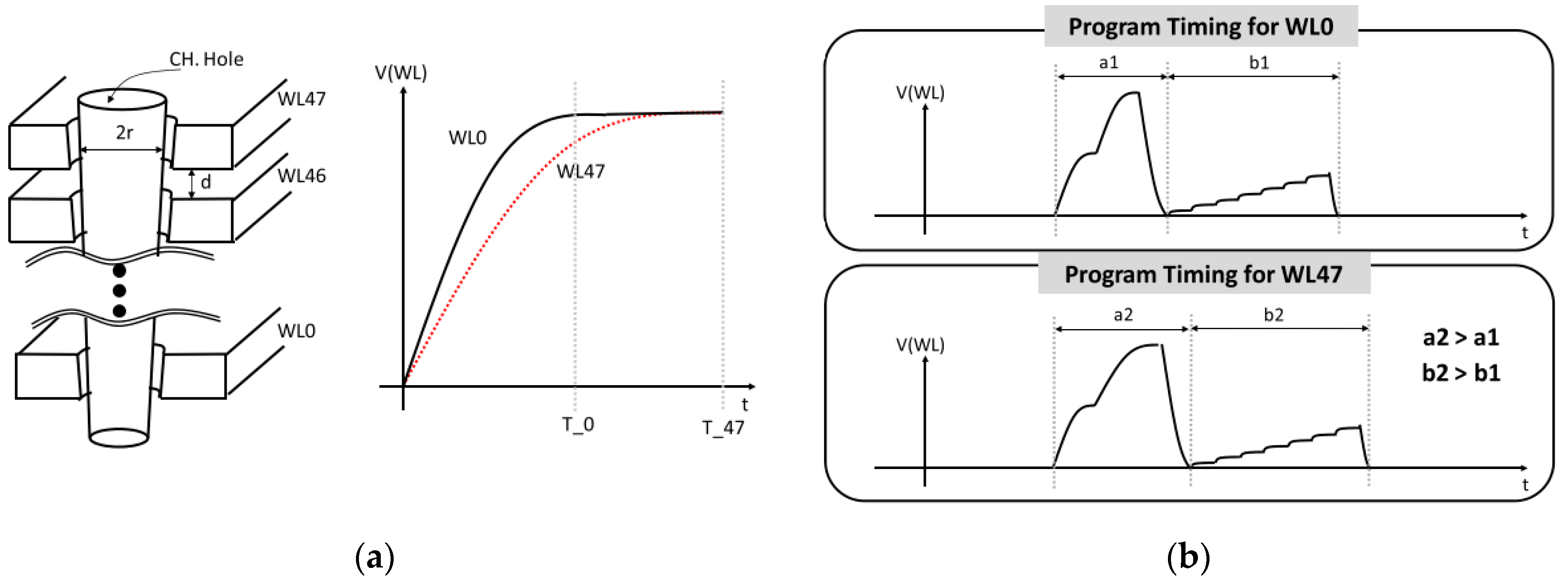
2.3. Cell Variation Improvement

In a 3D NAND flash memory, a gate electrode and an insulator are alternately stacked through a single etching process. Therefore, there is an advantage in that this process increases the manufacturing efficiency and enables continuous bit capacity increase. However, there are disadvantages in that the process causes a difference in the size of the channel hole critical dimensions (CD) between the upper and lower WLs and causes a variation between the hole CDs in the lower WL due to the limitations of the physical etching process [41]. Furthermore, as the number of WL stacks increases, it is necessary to reduce the physical height of the entire total stack to perform the hole etching process at once; thereby, pitch shrinking of gate electrode and insulating layer also become unavoidable engineering processes [10]. When the pitch of the WL layer is decreased, the resistance of individual WLs increases and the upper and lower WL-to-WL capacitances continuously increase [42]. In addition, the fringing field of adjacent WLs increases and the initial Vt is decreased, reducing the program speed [43]. Furthermore, since the charge trap layer is connected over the entire WLs, and because the distance between cells gets closer, the trap layer becomes more vulnerable to retention loss [5]. To solve the above cell variation problem caused by the geometry and process integration of 3D NAND, various programming improvement methods have been proposed.
First, to improve the size variation of hole CDs between WLs, different programming pulse widths are applied according to individual WLs [44], as shown in Figure 5. Due to the etching process, the resistance component increases toward the lower WL and the channel capacitance between the gate and the poly-silicon channel tends to decrease as well [42]. This difference between WLs causes loading variation between WLs, and the effective programming pulse width can fluctuate during a given pulse period. As it drops from the upper WL to the lower WL, a longer programming pulse is applied to keep the programming speed uniform among WLs.
A WL overdrive scheme was also proposed to overcome the WL RC delay variation caused by non-uniformity of the plug CD [45,46]. Considering WL RC Loading variation, delivering a verify pulse signal to the target Vt level within a given time is very challenging. The time and voltage offset can be controlled independently for each WL group; however, since too many degrees of freedom burden the entire circuit area of the chip, it may be a good idea to contain WLs in several grouping units considering the location of cells.
Due to the increased resistance of individual WLs and WL-WL capacitances by pitch shrink of stacked WLs, it is difficult to increase the programming voltage to the target Vt level, and power consumption increase. To solve this problem, T. Tanaka et al. suggested a method of applying the programming pulse by dividing it into two periods [47]. For the first period, selected and unselected WLs are raised to intermediate potential levels below their target levels. Then, the potential of the selected WL is increased by capacitive coupling to adjacent WLs that are also increased to their target level at the same time.
Meanwhile, boosting a single WL’s potential aided by adjacent WLs can cause a large glitch in the neighboring WLs as well as in the selected WL, and can result in an unintended program disturbance [48]. To resolve this problem, a glitch-canceling discharge scheme and a pre-offset control scheme have been proposed as methods to avoid capacitive coupling [49]. When the selected WL is programmed, the glitch can be generated in the adjacent WLn + 1, which can additionally cause the cell’s programed Vt variation. Thus, it is shown that the pass voltage of adjacent WL can be kept constant by preemptively lowering the target pass voltage level of the adjacent unselected WL.
As a similar concept to utilize the capacitive coupling, as shown in Figure 6, D. Kang et al. showed that programming throughput can be improved by applying the same verify voltage to WLn + 1 to reduce capacitive coupling during the verify operation of the selected WL [50]. This is because, before WLn + 1 is programmed, it stays in the erase state and applying a lower voltage than the read pass voltage to WLn + 1 does not affect the sensing current for the verify operation of the selected WL. However, in 3D NAND, since there is no metallurgical junction among WLs, the fringing field may induce Vt variation of the selected WL at read operation, depending on the voltage previously applied to adjacent WLs.
As the pitch of WLs is downward, the initial Vt of the selected WL decreases due to an increase in the fringing field of the adjacent WL during read operation, which decreases the programed Vt of the selected WL. To improve this, a method of applying a negative voltage to BL has been proposed [43]. Unlike the conventional method of applying ground to BL in the program operation, by applying a negative voltage, the voltage between the gate and the poly-silicon channel can be increased, and thus, more electrons can be programmed, widening the memory window. However, this method may also cause reliability problems, such as oxide breakdown by increasing the electric field between the gate and the channel and retention loss by trapping the excess electrons, and may burden the peripheral circuit for generating a negative voltage.
In the transition from 2D to 3D NAND, another problem in terms of reliability is early retention loss. Since 3D NAND uses band-engineered tunneling oxide for hole injection during the erase operation, electrons are not only stored in the charge trap layer in the program operation, but some are trapped in the tunneling oxide, weakening vertical retention characteristics [51,52]. Moreover, the electrons stored in the charge trap layer undergo lateral migration through silicon nitride connected over the entire WLs, intensifying retention loss [53,54]. To improve this, a reprogram method in which program operation is performed once again in a state where retention loss has occurred right after first program operation, improving both vertical and lateral charge loss [55]. As shown in Figure 7, the negative counter pulse scheme was also suggested [48]. This scheme utilizes a counter-pulse by boosting the channel potential through a self-boosting mechanism while applying a negative gate voltage to a selected WL during verifying operation, as shown in Figure 7. The large negative field generated accelerates the de-trap process between program loops, thereby reducing the retention loss.
A aggressive pitch scaling of WLs also results in cell-to-cell programed Vt variation due to hole radius variation by high aspect-ratio hole etching process, which increases the number of programming loops, degrading the program throughput. To solve this problem, an adaptive pulse programming scheme is proposed [56]. Programmed Cell Vt distribution can be reduced by classifying fast cells and slow cells in advance. By applying inhibit voltage to BL to induce program inhibit operation in fast cells during the program pulse, it prevents fast cells from over programming by using shorter programming pulse width. W-C. Chen et al. also proposed a pair-bitline program scheme. In the case of our single-gate vertical-channel (SGVC) 3-D NAND Flash chip, the gate edge profile causes strong discrepancy of program property between even or odd BLs. These issues are usually addressed by performing program on cells individually on even and odd BLs at the expense of program throughput. In the case of pair-BL PGM, by surrounding the adjacent pattern with two floating channels with boost potential, it improves the program efficiency of the slowest bit and address large cell-to-cell PGM variation caused by high aspect-ratio hole etching in 3D NAND Flash.
Furthermore, high aspect-ratio hole etching reduces the hole radius toward the lower WL and strengthens the electric field applied to the gate dielectric [57]. This increases the program speed of the lower WL, but further deteriorates WL-to-WL interference when the aggressor cell becomes the lower WL [58]. To improve this phenomenon, instead of programming from lower WL to upper WL, performing programming from upper WL to lower WL can greatly relieve the cell-to-cell interference between WLs [59].
On the other hand, there have been several system-level optimizations to address temperature and process-variation issues in 3D NAND flash memory. Y. Wang et al. suggested the temperature-aware data management scheme [60] and a process-variation-aware space allocation strategy [61] in the open-channel solid state drive (SSD), a hardware and file system interface that can allocate physical space to relieve the process variation of 3D NAND flash memory. Several optimization strategies have been proposed for open channel SSDs to prevent unreliable physical block usage, demonstrating that uncorrectable bit errors are reduced.

3. Read Algorithm

The read algorithm is described in three subsections. In Section 3.1, the two modes in which read disturbance occurs will be described, as will be improvement methods. In Section 3.2, the enhancement method to improve the read performance will be described and the improved read retry operation algorithm will be reviewed. Finally, Section 3.3 will describe various techniques to improve the read failure phenomenon caused by the variation and geometry of the 3D NAND process.

3.1. Improvement of Read Disturbance

To read the Vt of the selected WL from the 3D NAND array, the read voltage of the desired target level to the selected WL is applied and at the same time the pass voltage to the unselected WL is applied to cause current to flow through the entire string. Since the read voltage applied to the unselected WL is relatively approximately 3~4 V lower than the pass voltage used in the program operation, read disturbance does not occur during several read operations. However, in recent years, the users are demanding increased numbers of read operations; the already large block-size due to the increment of WL stacks and strings is also exponentially increasing the number of read pass voltages applied to individual cells. When read stress is applied hundreds of thousands of times, a soft programming read disturbance is generated by the potential difference between the poly-silicon channel and the gate, resulting in read failure [62].
A generally conceivable method to improve the soft programming read disturbance is to lower the read pass voltage: the string current of the cell is reduced and the sensing margin is also reduced, which deteriorates the read margin between the cell distributions, so this is not an appropriate engineering approach.
In 2D NAND, a self-boosting read scheme has been adopted to alleviate the above read disturbance, and was quickly applied to 3D NAND [63], as shown in Figure 8. In this technique, the read pass voltage of the unselected WL rises and, at the same time, the poly-silicon channel is also boosted by turning off the upper and lower select transistors in the unselected string by capacitive coupling. This effectively reduces the potential between the gate and the channel, improving the soft programming read disturbance. However, if the channel boosting level is too strong, HCI-related read disturbance phenomenon occurs [64,65]. As an example, the channel potential level of the unselected WL increases as the read pass voltage rises, whereas much lower read voltage or even a negative voltage (negative verify level) can be applied to the selected WL, so a strong transverse electric field is applied underneath the poly-silicon channel between selected WL and adjacent WLs. This accelerates BTBT tunneling current and generates electron-hole pairs, eventually inducing hot carrier injection toward the unselected WL. When the programed level is the highest in the selected WL, the worst HCI-related read disturbance can be provoked because the effective channel potential applied by the gate is the lowest.
To solve this problem, B.-I. Choe suggested a technique to apply shorter pulse widths to the upper and lower select transistors in the unselected string than the read pass pulses applied to unselected WLs, and to synchronizing both pulses at their rising edges [65]. With the proposed method, the channel boosting potential in the unselected string is drained, suppressing HCI-related read disturbance.
In addition, to reduce the electric field between the selected WL and the adjacent WLs by the high boosting level during the read operation, a method of lowering the read pass voltage of the adjacent WL was also proposed [66]. However, in this method, since the adjacent WL bias during the verify and read operations can be different, there is a possibility that the Vt of the read operation is shifted compared to that of the verify operation or that cell distribution widening may occur, and so an additional circuit to control this difference will be needed. Meanwhile, D. W. Kwon et al. found that a short “pre-turn on” pulse, just before applying the read voltage to the selected WL, will share the potential of the channel boosting area of the adjacent WL and the negative boosting area of the selected WL, such that the read disturbance is improved even in various worst program patterns [67]. However, this method can also cause read performance degradation by incurring extra read time.
To further improve the above problems, a reverse read scheme was proposed [44,62] (Figure 9). In conventional methods, the read voltage to the selected WL is applied sequentially from the low read level (R1) to the high read level (R3). Conversely, the proposed method reads from the high read level (R3) to the low read level (R1) on the selected WL. In this case, when a high read level is applied, the channel potential difference between selected WL and adjacent WLs decreases and the corresponding transverse electric field decreases. Besides this, during read phases R1 and R2, an electron was pulled from the selected WL to the adjacent unselected WLs’ channel due to potential difference, and so the transverse electric field is also reduced and the occurrence of HCI-related read disturbance can be reduced again. Reading the Vt first for the highest read level can also reduce the time required to reach the target voltage, therefore reducing WL setup time [42].

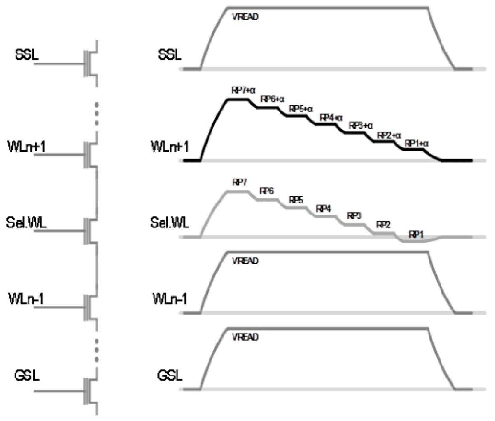
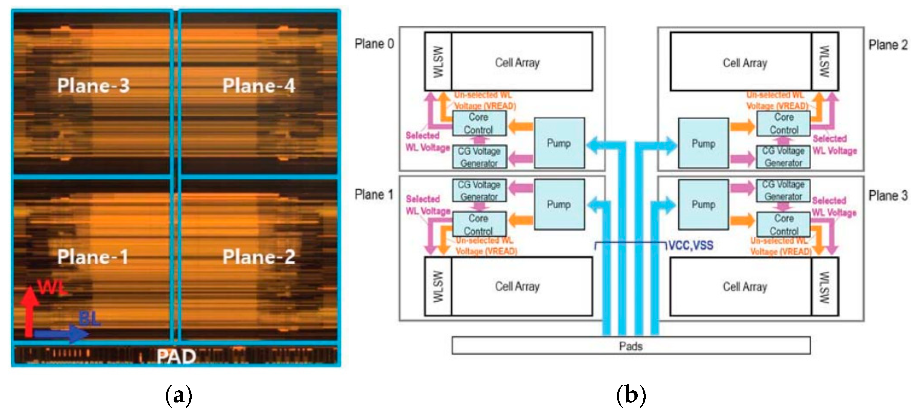
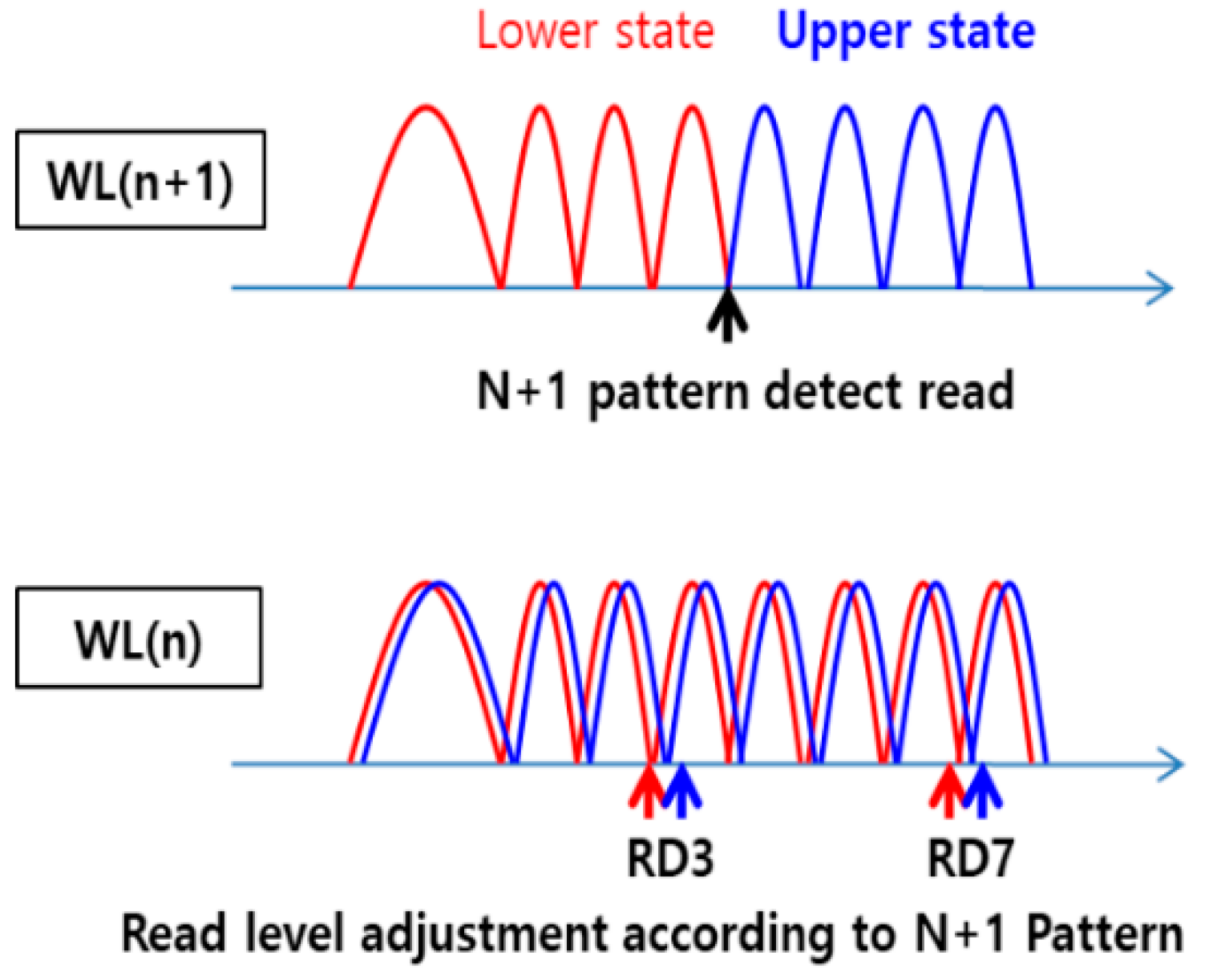
3.2. Improvement of Read Performance

Next, looking at the read algorithm and its relation to read performance improvement, the first step is to reduce the sequence and duration within one read operation cycle by optimizing the read operation conditions; the second step is to modify the chip architecture and cell design; and the third step is to improve the number of read operations through revision of the read retry algorithm.
First, to decrease the period of one read cycle, a method to reduce the BL pre-charge time has been proposed [50], increasing the BL pre-charge efficiency by permitting a continuous current flow in the page buffer circuit. Moreover, concurrent program sensing scheme has been proposed to reduce the sequence of read operations [63]. In conventional TLC NAND flash memory, two or three read voltage levels are applied and sensed within one read cycle, and BL pre-charge-evaluation-recovery operations are sequentially performed each time. In this paper, it is demonstrated that the total read time can be reduced by omitting the BL recovery operation of the second sensing operation and starting the second sensing operation with the first sensing, thereby retrieving the very long second evaluation time. Meanwhile, H. Huh et al. showed that the read noise can be improved by applying ground level to the adjacent BL when sensing the selected BL to improve cell distribution by reducing coupling noise caused by the adjacent BL [68]. However, in this case, an additional read time budget should be considered.
Second, there are several methods to improve the read performance by changing the chip architecture. For further read performance enhancement, parallel operation technology should be secured along with the aforementioned read period reduction within one read cycle. In 2D NAND, a two-plane architecture with 8 KB page size used to be the mainstream; however, as the field moved to 3D NAND, a two-plane architecture with 16 KB page size was adopted [47]. Currently, cell under array (CuA) technology has secured space for more page buffer circuits and sense amplifiers, and so four-plane architecture with 16 KB is applied to most 3D NAND products [30,31,46,63], as shown in Figure 10a; this parallel technology contributes to higher read and program performance [70]. For further improvement, an independent multi-plane read operation is proposed, in which each group of two or four planes can perform read operations independently and asynchronously on any block/page address, thereby improving system level read and write performances [69,71,72], as shown in Figure 10b. In addition, J.-W. Park et al. proposed a center-XDEC architecture and half-plane activation method [46]. Compared to the conventional edge-XDEC, the source of each local WL (referred to as global WL) is placed at the center of each plane for the center-XDEC. The local WL is activated by a bypass transistor, which is controlled by a block enable signal. This technique cuts the WL capacitance in half and reduces the WL RC loading, thereby decreasing WL settling time and increasing the random read performance.
Third, it is a method to reduce the read time overhead through revision of the read retry algorithm. Retrying a read can extend the lifetime of a NAND Flash memory; however, a performance degradation due to repetitive read operations is inevitable [73]. In 3D NAND, a cell distribution shift occurs over time due to repeated program/erase cycling and retention loss. In this case, when data are read at the previously fixed read level, the read margin is reduced, and thereby, the read failure rate is rapidly increased due to the above shift of cell distribution. To improve this, each NAND manufacturer finds repeatably a read level with an optimal read margin by applying a voltage near the read level initially set by each company’s read retry policy while changing the read voltage little by little. L. Lee et al. proposed a fast read retry scheme [37]. If the read voltage for detecting retention loss is below the default read voltage, the read level is lowered according to the predefined look-up table (LUT) of each state’s read level, thereby reducing the number of tracking cycles. A smart Vt -tracking read scheme has also been proposed [39]. This technique improves read retry performance by minimizing the tracking time and supporting a program suspend read function.

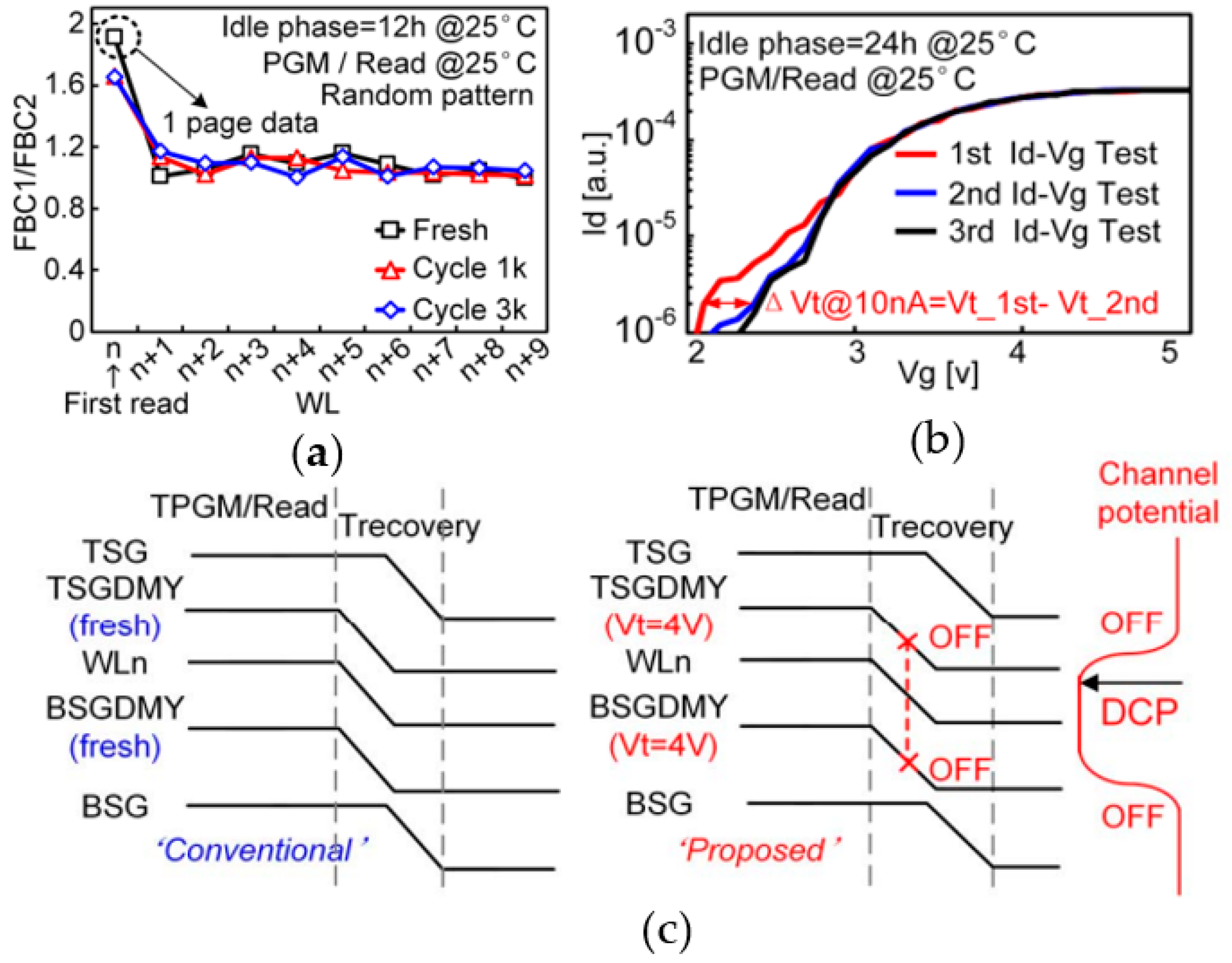
3.3. Read Failure Improvement

As previously described in the program algorithm, various solutions have been proposed to solve the cell reliability and variation problems caused by the geometry of the process integration technology of 3D NAND in the read operation.

3.3.1. The WL Pitch Scaling

Because cell-to-cell interference between WLs is a major source of increase of the read failure rate, several approaches have been derived. In NAND flash memory, since cells are arranged side by side, amount of Vt shift of a selected WL varies depending on the programming level of the adjacent WL [74]. In addition, after 1 block programming operation is completed, a charge shift occurs due to lateral migration toward the adjacent WL around the selected WL, aggravating the Vt shift [75].
To improve the above problem, W. Kim et al. proposed a read level adjustment method according to WLn + 1 Pattern [58], as shown in Figure 11. First, to broadly classify WLn + 1 pattern into two types, a pre-sensing operation is performed on WLn + 1. Next, since the amount of Vt shift of WLn varies according to the program level of WLn + 1, the read level of WLn is carefully adjusted. This method increases the read time overhead and the additional latch that stores the WLn + 1 pre-sensing result must be inserted [32].
J.-M. Sim et al. demonstrated that when reading the WLn, cell-to-cell interference can be greatly improved by adding an offset read bias of 1.5 V or more to adjacent WLs compared to unselected WL [76]. In general, cell-to-cell interference is worsen when the channel potential of WLn changes rapidly right after WLn + 1 is programmed. The proposed method keeps the channel potential fluctuation of WLn to a minimum even when WLn + 1 is programmed. However, this method causes soft programming read disturbs due to increases in read bias of adjacent WLs. To improve the charge loss caused by the reduced the pitch between WLs, D.-h. Kim et al. proposed an adaptive-read scheme [36]. First, they measure the number of cells in the highest state that are most likely to cause retention loss. When the page read command is invoked, the chip starts reading in the highest states and count the retention loss of the highest verify level cell in advance and then correct the bias of other lower read levels thereafter. This method improves the overall read margin.

3.3.2. Poly-Silicon Channel Effect

Several methods have been proposed to improve the abnormal read failure phenomenon caused by the grain boundary nature of the poly-silicon channel. Most abnormal read failure characteristics reported to date for poly-Si channels have been mainly caused by grain boundary traps (GBT). First, the problem caused by GBT is that the lower the temperature of the operating condition of the chip, the lower the channel current, which affects the sensing operation, deteriorating the cell distribution. In 2D NAND, using single crystalline silicon, phonon scattering decreases as the temperature decreases, and thereby increasing channel current [77]. However, when poly-silicon is used as a channel material, electrons are trapped at the grain boundary of poly-silicon and these trapped electrons forms a potential barrier, degrading the channel conductance. As the temperature is much lowered, the potential barrier for electrons becomes higher and higher and the channel current is further reduced, which deteriorates the sensing margin, causing read fail. As a way to improve this, a scheme to uniformly compensate for the channel current using an analog temp sensor that modulates the BL voltage in proportion to the external temperature was proposed [78]; it was demonstrated that cell distribution degradation was improved at low temperatures. However, in this method, there is a risk that the cell-to-cell interference is deteriorated during the read operation due to the neighboring gate-induced barrier lowering (NIBL) phenomenon [79]. On the other hand, as another method of compensating channel current at low temperature, a method of compensating for the pass voltage of unselected WL according to temperature has been proposed [80]. It was shown that read failure by Vt variation across temperature can be improved by increasing the pass voltage of the select transistor, which has a large effect on the channel current reduction. Compared to the previous BL voltage compensation scheme, in this new method, the NIBL phenomenon can be alleviated; however, if too high a pass voltage is applied at low temperature, it may cause a soft programming read disturbance, although the Fowler Nordheim (FN) tunneling current across the oxide is reduced at low temperature.
The second problem caused by GBT is the BL transient current phenomenon. In general, when a read voltage is applied between a channel and a gate during a read operation, band bending occurs in the poly-Si, and the poly-Si grain boundary trap below the fermi level tries to fill electrons with a high probability [81]. Therefore, as the read voltage is applied and electrons fill into these GBTs for a time of 1 msec, the channel current continuously decreases. To solve this phenomenon, W.-J. Tsai et al. proposed the ‘pre-condition’ voltage method to improve the transient current that occurs during the 1 msec immediately after the read voltage is applied to the selected WL [82]. However, becasue this method requires an additional pulse phase, there is a problem that the overall read performance deteriorates.
On the other hand, S. Xia et al. proposed a method to improve the read failure phenomenon that occurs only when the first selected WL is read after programming operation [83]. The physical mechanism is as follows. This phenomenon occurs during the idle period after the program operation is performed. During this idle time, electrons in the GBTs gradually discharge, because the gate voltage changes from program bias to 0 V [84], as shown in Figure 12. During the first read operation, the previous discharged GBTs cause lower cell Vt. After the first read operation, previous discharged GBTs are refilled due to the applied read bias, and then return to the original Vt state. To improve this, in a conventional method, after the program operation is finished, the voltages of the upper and lower dummy WLs changes from the pass voltage to 0 V; however, by holding the dummy WL bias at 4 V (Vt = 4 V), the down coupling phenomenon is suppressed and the electrons in the GBTs do not discharge [84].

4. Erase Algorithm

Unlike the program and read operations described above, the erase operation is difficult to disturb because block erase operation is performed. Also, since the operation time is very long compared to the program operation, the performance criterion is also relatively less intensive than that of the program/read operation. Therefore, most of the erase operation algorithms are focused on improving cell reliability or cell variation rather than improving the performance.

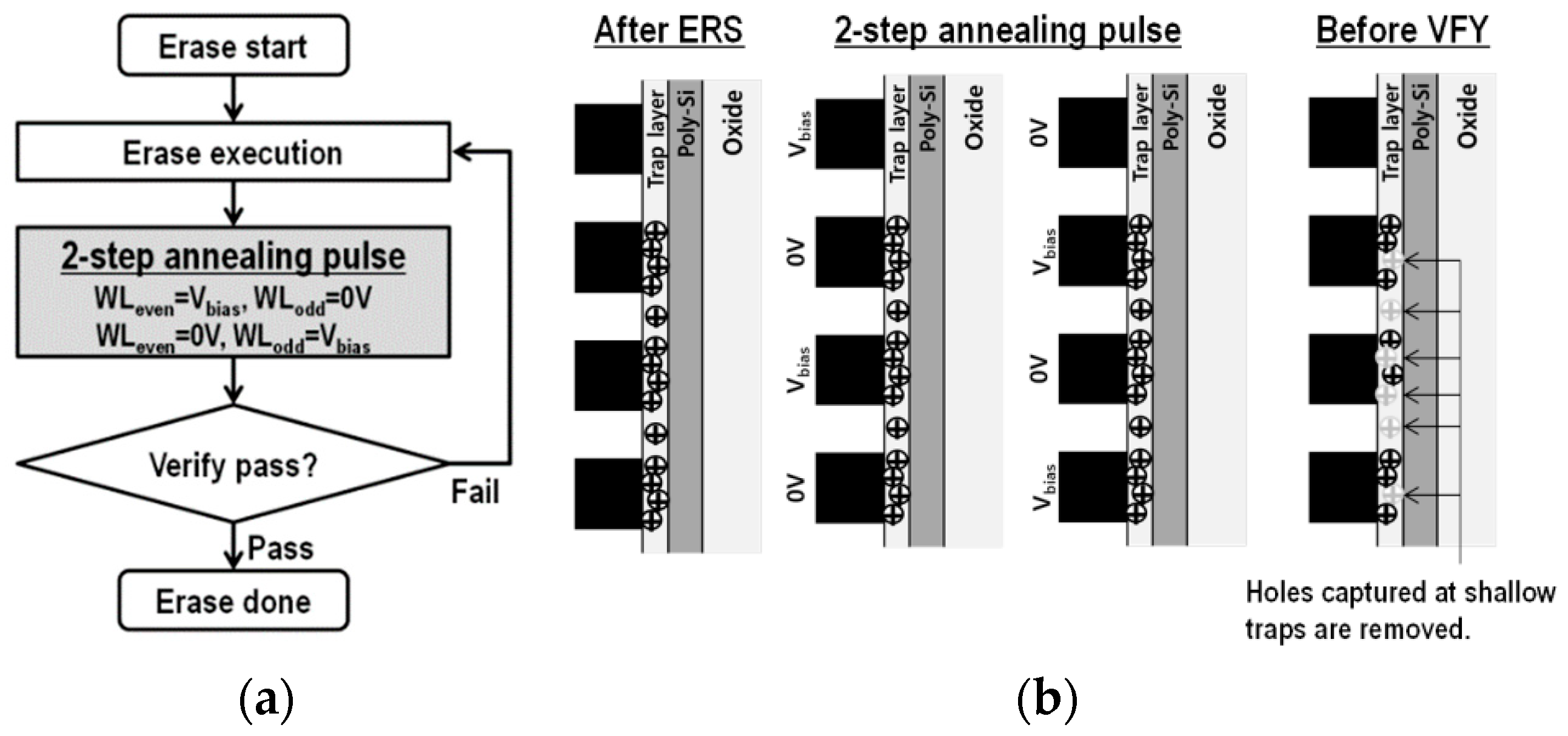
4.1. Improving the Effect of Lateral Migration

In 3D NAND, the charge trap layer (CTL) is entirely connected, from the upper WL to the lower WL, and so charges are also trapped in the CTL in the spaces between WLs during repetitive program/erase cycling [85]. In addition, since 3D NAND forms a virtual junction by fringing field, the Vt of the cell is sensitively affected not only by the charges stored in the CTL but also by the charge in the space region. In particular, as the WL pitch becomes smaller and smaller, more holes are programmed in the CTL in the space region during the erase operation due to an increase in the fringing field by the adjacent WLs. This leads to an acceleration of retention loss due to the lateral migration effect.
To improve the above problems, C. Kim et al. proposed a two-step annealing pulse scheme [40], shown in Figure 13. In conventional NAND, the equivalent voltage (0 V) is applied to all WLs when the erase voltage is applied to the channel during erase operation. However, in the proposed method, at first, 0 V is applied to even WLs, while biasing odd WLs. Next, 0 V is reversely applied to odd WLs while biasing even WLs. It is demonstrated that retention loss can be improved by suppressing the formation of holes by the fringing field in the space region. However, in this case, the two-step erase operation can deteriorate the erase time, and so there is a trade-off between erase performance and reliability gain, which must be carefully controlled.
Whereas the above-mentioned approach minimizes the occurrence of hole traps in the space area, D.-H. Kim et al. proposed a deep erase compensation scheme to reduce holes under the gate [36]. Recently, holes underneath adjacent WLs, as well as holes in the space area, have been reported to critically deteriorate the lateral migration effect [86]. In the proposed method, by softly verifying the deep erased cells toward the high Vt, retention loss by lateral migration can be enhanced. However, in this method, if the soft verifying sequence is added to all WLs within the entire erase operation, the erase time becomes too long. Therefore, adding this sequence to the program operation would be a more realistic solution.

4.2. Reliability Improvement

As described above, the block size of 3D NAND is continuously enlarging to further increase the bit density. However, since erase operations are also performed in units of blocks, these operations burden system-level reliability. To improve this problem, a block-by-deck (BBD) concept was proposed [72]. In this method, the entire WL is divided into three decks and when the erase operation is performed, individual bias is applied to the WL of each deck so that the erase operation is performed separately for each deck. In this way, the reliability of the chip can be improved because one physical block is composed of three logical sub-blocks. However, in this method, since the erase operation and the erase inhibition must be performed at the same time, a strong transverse electric field is applied between the decks, which is likely to cause hot carrier injection disturbance. Therefore, arranging optimal dummy WLs between the decks is an important procedure.
L. Yan et al. reported that, because of repetitive erase operation, program disturbance may occur due to cycling-induced Vt shift of the top select transistor (TST) [87]. During the erase operation, when high voltage is applied to SL and BL and 0 V is applied to the TST gate, a hot hole is generated by the strong transverse electric field applied under the channel between the dummy WLs and the TST. Then, hot holes break the Si-H bonds at the poly-Si/SiO2 interface, leading to TST Vt shift. The transverse electric field is alleviated by pushing a positive voltage to the TST after a certain point when SL and BL are rising. However, if the voltage gap between TST and BL and SL is too small, GIDL current generation is reduced and the erase speed may be degraded. Therefore, the trade-off relationship between reliability and erase performance must be carefully adjusted.
J. K. Park proposed a method of applying a small positive pulse immediately after the erase operation to overcome the Vt transient phenomenon [88]. In this study, vertical redistribution of holes at interface between CTL and blocking oxide toward the tunnel oxide direction continuously decreases the erased Vt, and increases the error bit in the erase verification operation. By applying a small positive pulse immediately after the erase pulse, increment in error bit can be reduced because the hole redistribution rapidly settled down.

4.3. Cell Variation Improvement

As shown in the previous description of program operation, several similar techniques in the erase operation have been proposed to improve cell variation caused by 3D NAND process. An on-chip erase speed detection method has been proposed to improve the problem that the erase speed increases toward the lower WL due to the electric field concentration effect [57]. This is because when the coaxial capacitor is biased, the electric field on the inner surface is greater than the electric field on the outer surface according to Gauss’s law. Before actual erase operation is performed, a pre-erase pulse is applied to check the erase speed for each WL, and an offset bias is automatically applied to each WL to erase all WLs toward the desired target Vt level. However, this method also adds erase time overhead, so a method to reduce the time overhead, such as correcting the erase speed at the wafer-level test stage, not during chip operation, is needed.
Meanwhile, D. Kang et al. proposed a method to maintain the entire PE window by lowering the Program verify level toward the lower WL without correcting the erase speed variation for each WL [50]. This method has the advantage of not requiring additional time, such as the pre-erase pulse above, but retention loss is likely to become more severe as it descends to the lower WL, because the retention characteristic is dominated by number of holes in the CTL (i.e., erased Vt) [85].

5. Conclusions

In the past few years, 3D NAND has steadily replaced 2D NAND in the non-volatile memory market and has become firmly established as the mainstream memory technology. In this paper, various operation algorithms and design techniques to improve the cell characteristics and performance in terms of Program, Read, and Erase operations, which are the basic operations of 3D NAND Flash memory, were reviewed. Furthermore, numerous methods to improve cell variation and reliability problems caused by 3D NAND process and geometry were described. All algorithms have advantages and disadvantages, because using a specific operation algorithm or technique may improve the individual characteristics of the device, but is highly likely to be detrimental in terms of chip area, overall system level performance, and device reliability. Nevertheless, to continue the trend of the last few years of increasing the bit density of 3D NAND, it is necessary to further develop various operation algorithms and chip design techniques mentioned in this paper, along with new process and material innovations.

Author Contributions

Investigation, J.K.P.; writing—original draft preparation, J.K.P.; writing—review and editing, S.E.K.; funding acquisition, S.E.K. All authors have read and agreed to the published version of the manuscript.

Funding

This research was supported by the National R&D Program through the National Research Foundation of Korea (NRF) funded by the Ministry of Science and ICT (2022M3I7A4072293).

Institutional Review Board Statement

Not applicable.

Informed Consent Statement

Informed consent was obtained from all subjects involved in the study.

Data Availability Statement

Not applicable.

Conflicts of Interest

The authors declare no conflict of interest.

References

  1. Park, Y.; Lee, J.; Cho, S.S.; Jin, G.; Jung, E. Scaling and reliability of NAND flash devices. In Proceedings of the 2014 IEEE International Reliability Physics Symposium, Waikoloa, HI, USA, 1–4 June 2014; pp. 2E. 1.1–2E. 1.4. [Google Scholar]
  2. Kim, H.; Ahn, S.-J.; Shin, Y.G.; Lee, K.; Jung, E. Evolution of NAND Flash Memory: From 2D to 3D as a Storage Market Leader. In Proceedings of the 2017 IEEE International Memory Workshop (IMW), Monterey, CA, USA, 14–17 May 2017. [Google Scholar]
  3. Yosuke, K.; Masaru, K.; Masaru, K.; Ryota, K.; Yoshiaki, F.; Hiroyasu, T.; Yuzo, N.; Megumi, I.; Hideaki, A.; Akihiro, N. Disturbless flash memory due to high boost efficiency on BiCS structure and optimal memory film stack for ultra high density storage device. In Proceedings of the 2008 IEEE International Electron Devices Meeting, San Francisco, CA, USA, 15 December 2008. [Google Scholar]
  4. Lee, J.; Jang, J.; Lim, J.; Shin, Y.G.; Lee, K.; Jung, E. A new ruler on the storage market: 3D-NAND flash for high-density memory and its technology evolutions and challenges on the future. In Proceedings of the 2016 IEEE International Electron Devices Meeting (IEDM), San Francisco, CA, USA, 3–7 December 2016. [Google Scholar]
  5. Kang, J.-K.; Lee, J.; Yim, Y.; Park, S.; Kim, H.S.; Cho, E.S.; Kim, T.; Lee, J.H.; Kim, J.; Lee, R.; et al. Highly Reliable Cell Characteristics with CSOB(Channel-hole Sidewall ONO Butting) Scheme for 7th Generation 3D-NAND. In Proceedings of the 2021 IEEE International Electron Devices Meeting (IEDM), San Francisco, CA, USA, 11 December 2021. [Google Scholar]
  6. Goda, A. Recent Progress on 3D NAND Flash Technologies. Electronics 2021, 10, 3156. [Google Scholar] [CrossRef]
  7. Kim, S.S.; Yong, S.K.; Kim, W.; Kang, S.; Park, H.W.; Yoon, K.J.; Sheen, D.S.; Lee, S.; Hwang, C.S. Review of Semiconductor Flash Memory Devices for Material and Process Issues. Adv. Mater. 2022, 2200659. [Google Scholar] [CrossRef] [PubMed]
  8. Micheloni, R.; Crippa, L.; Zambelli, C.; Olivo, P. Architectural and Integration Options for 3D NAND Flash Memories. Computers 2017, 6, 27. [Google Scholar] [CrossRef] [Green Version]
  9. Lee, G.H.; Hwang, S.; Yu, J.; Kim, H. Architecture and process integration overview of 3D NAND flash technologies. Appl. Sci. 2021, 11, 6703. [Google Scholar] [CrossRef]
  10. Alsmeier, J.; Higashitani, M.; Paak, S.S.; Sivaram, S. Past and Future of 3D Flash. In Proceedings of the 2020 IEEE International Electron Devices Meeting (IEDM), San Francisco, CA, USA, 12–18 December 2020. [Google Scholar]
  11. Goda, A. 3-D NAND Technology Achievements and Future Scaling Perspectives. IEEE Trans. Electron Devices 2020, 67, 1373–1381. [Google Scholar] [CrossRef]
  12. Keon-Soo, S.; Eun-Seok, C.; Sung-Wook, J.; Se-Hoon, K.; Hyun-Seung, Y.; Kwang-Sun, J.; Han-Soo, J.; Jung-Seok, O.; Yoon-Soo, J.; Kyung-Jin, P.; et al. Inherent Issues and Challenges of Program Disturbance of 3D NAND Flash Cell. In Proceedings of the 2012 4th IEEE International Memory Workshop, Milan, Italy, 20–23 May 2012. [Google Scholar]
  13. Cho, J.; Kimpton, D.; Guichard, E. Optimization of select gate transistor in advanced 3D NAND memory cell. In Proceedings of the 2019 International Conference on Simulation of Semiconductor Processes and Devices (SISPAD), Udine, Italy, 4–6 September 2019. [Google Scholar]
  14. Kwon, D.W.; Kim, W.; Kim, D.-B.; Lee, S.-H.; Seo, J.Y.; Baek, M.-H.; Park, J.-H.; Choi, E.; Cho, G.S.; Park, S.-K.; et al. Analysis on Program Disturbance in Channel-Stacked NAND Flash Memory With Layer Selection by Multilevel Operation. IEEE Trans. Electron Devices 2016, 63, 1041–1046. [Google Scholar] [CrossRef]
  15. Seo, J.Y.; Kim, Y.; Park, B.-G. New program inhibition scheme for high boosting efficiency in three-dimensional NAND array. Jpn. J. Appl. Phys. 2014, 53, 070304. [Google Scholar] [CrossRef]
  16. Kang, M.; Kim, Y. Natural Local Self-Boosting Effect in 3D NAND Flash Memory. IEEE Electron Device Lett. 2017, 38, 1236–1239. [Google Scholar] [CrossRef]
  17. Zhang, Y.; Jin, L.; Jiang, D.; Zou, X.; Zhao, Z.; Gao, J.; Zeng, M.; Zhou, W.; Tang, Z.; Huo, Z. Leakage characterization of top select transistor for program disturbance optimization in 3D NAND flash. Solid State Electron. 2018, 141, 18–22. [Google Scholar] [CrossRef]
  18. Han, S.; Jeong, Y.; Jhon, H.; Kang, M. Investigation of Inhibited Channel Potential of 3D NAND Flash Memory According to Word-Line Location. Electronics 2020, 9, 268. [Google Scholar] [CrossRef]
  19. Kim, Y.; Kang, M. Down-coupling phenomenon of floating channel in 3D NAND flash memory. IEEE Electron Device Lett. 2016, 37, 1566–1569. [Google Scholar] [CrossRef]
  20. Raghunathan, S. (Invited) 3D-NAND Reliability: Review of key mechanisms and mitigations. In Proceedings of the 2020 4th IEEE Electron Devices Technology & Manufacturing Conference (EDTM), Penang, Malaysia, 6–21 April 2020. [Google Scholar]
  21. Yamashita, R.; Magia, S.; Higuchi, T.; Yoneya, K.; Yamamura, T.; Mizukoshi, H.; Zaitsu, S.; Yamashita, M.; Toyama, S.; Kamae, N.; et al. 11.1 A 512Gb 3b/cell flash memory on 64-word-line-layer BiCS technology. In Proceedings of the 2017 IEEE International Solid-State Circuits Conference (ISSCC), San Francisco, CA, USA, 5–9 February 2017.
  22. Zhang, Y.; Jin, L.; Zou, X.; Liu, H.; Zhang, A.; Huo, Z. A Novel Program Scheme for Program Disturbance Optimization in 3-D NAND Flash Memory. IEEE Electron Device Lett. 2018, 39, 959–962. [Google Scholar] [CrossRef]
  23. Wang, J.; Wang, M. Separation of the geometric current in charge pumping measurement of polycrystalline Si thin-film transistors. IEEE Trans. Electron Devices 2014, 61, 4113–4119. [Google Scholar] [CrossRef]
  24. Caillat, C.; Beaman, K.; Bicksler, A.; Camozzi, E.; Ghilardi, T.; Huang, G.; Liu, H.; Liu, Y.; Mao, D.; Mujumdar, S.; et al. 3DNAND GIDL-Assisted Body Biasing for Erase Enabling CMOS under Array (CUA) Architecture. In Proceedings of the 2017 IEEE International Memory Workshop (IMW), Monterey, CA, USA, 14–17 May 2017. [Google Scholar]
  25. Jeong, Y.; Ham, I.; Han, S.; Kang, M. Optimal dummy word line condition to suppress hot carrier injection phenomenon due to the natural local self-boosting effect in 3D NAND flash memory. Jpn. J. Appl. Phys. 2020, 59, SGGB17. [Google Scholar] [CrossRef]
  26. Chen, W.-C.; Lue, H.-T.; Hsieh, C.-C.; Wang, K.-C.; Lu, C.-Y. Performance enhancement of 3-D NAND flash featuring a two-step dummy wordline program waveform and pair-bitline program scheme. IEEE Trans. Electron Devices 2020, 67, 99–104. [Google Scholar] [CrossRef]
  27. Lin, W.-L.; Tsai, W.-J.; Cheng, C.C.; Lu, C.-C.; Ku, S.H.; Chang, Y.W.; Wu, G.-W.; Liu, L.; Hwang, S.W.; Lu, T.-C.; et al. Hot-Carrier Injection-Induced Disturb and Improvement Methods in 3D NAND Flash Memory. In Proceedings of the 2019 International Symposium on VLSI Technology, Systems and Application (VLSI-TSA), Hsinchu, Taiwan, 22–25 April 2019. [Google Scholar]
  28. Yoon, C.-W. The Fundamentals of NAND Flash Memory: Technology for tomorrow’s fourth industrial revolution. IEEE Solid-State Circuits Mag. 2022, 14, 56–65. [Google Scholar] [CrossRef]
  29. Chang, Y.-M.; Chang, Y.-H.; Kuo, T.-W.; Li, Y.-C.; Li, H.-P. Disturbance Relaxation for 3D Flash Memory. IEEE Trans. Comput. 2016, 65, 1467–1483. [Google Scholar] [CrossRef]
  30. Yuh, J.; Li, J.; Li, H.; Oyama, Y.; Hsu, C.; Anantula, P.; Jeong, S.; Amarnath, A.; Darne, S.; Bhatia, S.; et al. A 1-Tb 4b/Cell 4-Plane 162-Layer 3D Flash Memory With a 2.4-Gb/s I/O Speed Interface. In Proceedings of the 2022 IEEE International Solid-State Circuits Conference (ISSCC), San Francisco, CA, USA, 20–24 February 2022. [Google Scholar]
  31. Pekny, T.; Vu, L.; Tsai, J.; Srinivasan, D.; Yu, E.; Pabustan, J.; Xu, J.; Deshmukh, S.; Chan, K.-F.; Piccardi, M.; et al. A 1-Tb Density 4b/Cell 3D-NAND Flash on 176-Tier Technology with 4-Independent Planes for Read using CMOS-Under-the-Array. In Proceedings of the 2022 IEEE International Solid-State Circuits Conference (ISSCC), San Francisco, CA, USA, 20–24 February 2022. [Google Scholar]
  32. Kim, M.; Yun, S.W.; Park, J.; Park, H.K.; Lee, J.; Kim, Y.S.; Na, D.; Choi, S.; Song, Y.; Lee, J.; et al. A 1Tb 3b/Cell 8th-Generation 3D-NAND Flash Memory with 164 MB/s Write Throughput and a 2.4 Gb/s Interface. In Proceedings of the 2022 IEEE International Solid-State Circuits Conference (ISSCC), San Francisco, CA, USA, 20–24 February 2022. [Google Scholar]
  33. Shibata, N.; Maejima, H.; Isobe, K.; Iwasa, K.; Nakagawa, M.; Fujiu, M.; Shimizu, T.; Honma, M.; Hoshi, S.; Kawaai, T.; et al. A 70 nm 16 Gb 16-Level-Cell NAND flash Memory. IEEE J. Solid-State Circuits 2008, 43, 929–937. [Google Scholar] [CrossRef]
  34. Im, J.-W.; Jeong, W.-P.; Kim, D.-H.; Nam, S.-W.; Shim, D.-K.; Choi, M.-H.; Yoon, H.-J.; Kim, D.-H.; Kim, Y.-S.; Park, H.-W.; et al. 7.2 A 128Gb 3b/cell V-NAND flash memory with 1 Gb/s I/O rate. In Proceedings of the 2015 IEEE International Solid-State Circuits Conference-(ISSCC) Digest of Technical Papers, San Francisco, CA, USA, 22–26 February 2015. [Google Scholar]
  35. Jeong, W.; Im, J.-W.; Kim, D.-H.; Nam, S.-W.; Shim, D.-K.; Choi, M.-H.; Yoon, H.-J.; Kim, D.-H.; Kim, Y.-S.; Park, H.-W.; et al. A 128 Gb 3b/cell V-NAND Flash Memory With 1 Gb/s I/O Rate. IEEE J. Solid-State Circuits 2016, 51, 204–212. [Google Scholar] [CrossRef]
  36. Kim, D.-H.; Kim, H.; Yun, S.; Song, Y.; Kim, J.; Joe, S.-M.; Kang, K.-H.; Jang, J.; Yoon, H.-J.; Lee, K.; et al. 13.1 A 1Tb 4b/cell NAND Flash Memory with tPROG = 2 ms, tR = 110 µs and 1.2 Gb/s High-Speed IO Rate. In Proceedings of the 2020 IEEE International Solid-State Circuits Conference-(ISSCC), San Francisco, CA, USA, 16–20 February 2020. [Google Scholar]
  37. Lee, S.; Kim, C.; Kim, M.; Joe, S.-M.; Jang, J.; Kim, S.; Lee, K.; Kim, J.; Park, J.; Lee, H.-J.; et al. A 1Tb 4b/cell 64-stacked-WL 3D NAND flash memory with 12 MB/s program throughput. In Proceedings of the 2018 IEEE International Solid-State Circuits Conference-(ISSCC), San Francisco, CA, USA, 11–15 February 2018. [Google Scholar]
  38. Dong, G.; Xie, N.; Zhang, T. On the Use of Soft-Decision Error-Correction Codes in nand Flash Memory. IEEE Trans. Circuits Syst. I Regul. Pap. 2011, 58, 429–439. [Google Scholar] [CrossRef]
  39. Maejima, H.; Kanda, K.; Fujimura, S.; Takagiwa, T.; Ozawa, S.; Sato, J.; Shindo, Y.; Sato, M.; Kanagawa, N.; Musha, J.; et al. A 512Gb 3b/Cell 3D flash memory on a 96-word-line-layer technology. In Proceedings of the 2018 IEEE International Solid-State Circuits Conference-(ISSCC), San Francisco, CA, USA, 11–15 February 2018. [Google Scholar]
  40. Kim, C.; Kim, D.H.; Jeong, W.; Kim, H.J.; Park, I.H.; Park, H.W.; Lee, J.; Park, J.; Ahn, Y.L.; Lee, J.Y.; et al. A 512Gb 3b/cell 64-Stacked WL 3D V-NAND Flash Memory. IEEE J. Solid State Circuits 2017, 53, 124–133. [Google Scholar] [CrossRef]
  41. Kim, J.H.; Yim, Y.; Lim, J.; Kim, H.S.; Cho, E.S.; Yeo, C.; Lee, W.; You, B.; Lee, B.; Kang, M. Highly Manufacturable 7 th Generation 3D NAND Flash Memory with COP structure and Double Stack Process. In Proceedings of the 2021 Symposium on VLSI Technology, Hsinchu, Taiwan, 13–19 June 2021; pp. 1–2. [Google Scholar]
  42. Kang, D.; Jeong, W.; Kim, C.; Kim, D.-H.; Cho, Y.S.; Kang, K.-T.; Ryu, J.; Kang, K.-M.; Lee, S.; Kim, W.; et al. 256 Gb 3b/cell V-NAND flash memory with 48 stacked WL layers. In Proceedings of the 2016 IEEE International Solid-State Circuits Conference-(ISSCC), San Francisco, CA, USA, 31 January–4 February 2016. [Google Scholar]
  43. Sim, J.-M.; Kang, M.; Song, Y.-H. A Novel Program Operation Scheme With Negative Bias in 3-D NAND Flash Memory. IEEE Trans. Electron Devices 2021, 68, 6112–6117. [Google Scholar] [CrossRef]
  44. Kang, D.; Jeong, W.; Kim, C.; Kim, D.-H.; Cho, Y.S.; Kang, K.-T.; Ryu, J.; Kang, K.-M.; Lee, S.; Kim, W.; et al. 256 Gb 3 b/Cell V-nand Flash Memory With 48 Stacked WL Layers. IEEE J. Solid-State Circuits 2017, 52, 210–217. [Google Scholar] [CrossRef]
  45. Shibata, N.; Kanda, K.; Shimizu, T.; Nakai, J.; Nagao, O.; Kobayashi, N.; Miakashi, M.; Nagadomi, Y.; Nakano, T.; Kawabe, T.; et al. A 1.33Tb 4-bit/Cell 3D-Flash Memory on a 96-Word-Line-Layer Technology. IEEE J. Solid State Circuits 2019, 55, 178–188. [Google Scholar] [CrossRef]
  46. Park, J.-W.; Kim, D.; Ok, S.; Park, J.; Kwon, T.; Lee, H.; Lim, S.; Jung, S.-Y.; Choi, H.; Kang, T.; et al. 30.1 A 176-Stacked 512Gb 3b/Cell 3D-NAND Flash with 10.8Gb/mm2 Density with a Peripheral Circuit Under Cell Array Architecture. In Proceedings of the 2021 IEEE International Solid-State Circuits Conference (ISSCC), San Francisco, CA, USA, 13–22 February 2021. [Google Scholar]
  47. Tanaka, T.; Helm, M.; Vali, T.; Ghodsi, R.; Kawai, K.; Park, J.-K.; Yamada, S.; Pan, F.; Einaga, Y.; Ghalam, A.; et al. 7.7 A 768Gb 3b/cell 3D-floating-gate NAND flash memory. In Proceedings of the 2016 IEEE International Solid-State Circuits Conference (ISSCC), San Francisco, CA, USA, 31 January–4 February 2016. [Google Scholar]
  48. Park, K.-T.; Nam, S.; Kim, D.; Kwak, P.; Lee, D.; Choi, Y.-H.; Choi, M.-H.; Kwak, D.-H.; Kim, D.-H.; Kim, M.-S.; et al. Three-Dimensional 128 Gb MLC Vertical nand Flash Memory With 24-WL Stacked Layers and 50 MB/s High-Speed Programming. IEEE J. Solid-State Circuits 2015, 50, 204–213. [Google Scholar] [CrossRef]
  49. Park, K.-T.; Han, J.-M.; Kim, D.; Nam, S.; Choi, K.; Kim, M.-S.; Kwak, P.; Lee, D.; Choi, Y.-H.; Kang, K.-M.; et al. 19.5 Three-dimensional 128Gb MLC vertical NAND Flash-memory with 24-WL stacked layers and 50 MB/s high-speed programming. In Proceedings of the 2014 IEEE International Solid-State Circuits Conference-(ISSCC), San Francisco, CA, USA, 9–13 February 2014. [Google Scholar]
  50. Kang, D.; Kim, M.; Jeon, S.C.; Jung, W.; Park, J.; Choo, G.; Shim, D.-K.; Kavala, A.; Kim, S.-B.; Kang, K.-M.; et al. 13.4 A 512Gb 3-bit/Cell 3D 6th-Generation V-NAND Flash Memory with 82 MB/s Write Throughput and 1.2 Gb/s Interface. In Proceedings of the 2019 IEEE International Solid-State Circuits Conference-(ISSCC), San Francisco, CA, USA, 17–21 February 2019. [Google Scholar]
  51. Chen, C.-P.; Lue, H.-T.; Hsieh, C.-C.; Chang, K.-P.; Hsieh, K.-Y.; Lu, C.-Y. Study of fast initial charge loss and it’s impact on the programmed states Vt distribution of charge-trapping NAND Flash. In Proceedings of the 2010 International Electron Devices Meeting, San Francisco, CA, USA, 6–8 December 2010; pp. 5.6.1–5.6.4. [Google Scholar]
  52. Ouyang, Y.; Xia, Z.; Yang, T.; Shi, D.; Zhou, W.; Huo, Z. Optimization of performance and reliability in 3D NAND flash memory. IEEE Electron Device Lett. 2020, 41, 840–843. [Google Scholar] [CrossRef]
  53. Maconi, A.; Arreghini, A.; Compagnoni, C.M.; Spinelli, A.; Van Houdt, J.; Lacaita, A.L. Comprehensive investigation of the impact of lateral charge migration on retention performance of planar and 3D SONOS devices. Solid State Electron. 2012, 74, 64–70. [Google Scholar] [CrossRef]
  54. Padovani, A.; Pesic, M.; Kumar, M.A.; Blomme, P.; Subirats, A.; Vadakupudhupalayam, S.; Baten, Z.; Larcher, L. Understanding and variability of lateral charge migration in 3D CT-NAND flash with and without band-gap engineered barriers. In Proceedings of the 2019 IEEE International Reliability Physics Symposium (IRPS), Monterey, CA, USA, 31 March–4 April 2019; pp. 1–8. [Google Scholar]
  55. Cheng, T.; Jia, J.; Jin, L.; Jia, X.; Xia, S.; Lu, J.; Li, K.; Luo, Z.; Li, D.; Liu, H.; et al. Investigation of Re-Program Scheme in Charge Trap-Based 3D NAND Flash Memory. IEEE J. Electron Devices Soc. 2021, 9, 640–644. [Google Scholar] [CrossRef]
  56. Du, Z.; Li, S.; Wang, Y.; Fu, X.; Liu, F.; Wang, Q.; Huo, Z. Adaptive Pulse Programming Scheme for Improving the Vth Distribution and Program Performance in 3D NAND Flash Memory. IEEE J. Electron Devices Soc. 2021, 9, 102–107. [Google Scholar] [CrossRef]
  57. Hsu, T.-H.; Lue, H.-T.; Lai, E.-K.; Hsieh, J.-Y.; Wang, S.-Y.; Yang, L.-W.; King, Y.-C.; Yang, T.; Chen, K.-C.; Hsieh, K.-Y. A high-speed BE-SONOS NAND flash utilizing the field-enhancement effect of FinFET. In Proceedings of the 2007 IEEE International Electron Devices Meeting, Washington, DC, USA, 6–8 December 2007; pp. 913–916. [Google Scholar]
  58. Kim, W.; Byeon, D.; Joe, S.-M.; Lee, J.; Song, J.H. Cell Operation Technologies to Overcome Scale-down Issues in 3D NAND Flash Memory. In Proceedings of the 2022 International Conference on Electronics, Information, and Communication (ICEIC), Jeju, Korea, 3–5 September 2022; pp. 298–299. [Google Scholar]
  59. Yi, S.-I.; Kim, J. Novel Program Scheme of Vertical NAND Flash Memory for Reduction of Z-Interference. Micromachines 2021, 12, 584. [Google Scholar] [CrossRef]
  60. Wang, Y.; Tan, J.; Mao, R.; Li, T. Temperature-Aware Persistent Data Management for LSM-Tree on 3-D NAND Flash Memory. IEEE Trans. Comput. Aided Des. Integr. Circuits Syst. 2020, 39, 4611–4622. [Google Scholar] [CrossRef]
  61. Wang, Y.; Huang, J.; Chen, J.; Mao, R. PVSensing: A Process-Variation-Aware Space Allocation Strategy for 3D NAND Flash Memory. IEEE Trans. Comput. Aided Des. Integr. Circuits Syst. 2022, 41, 1302–1315. [Google Scholar] [CrossRef]
  62. Zhang, Y.; Jin, L.; Jiang, D.; Zou, X.; Liu, H.; Huo, Z. A Novel Read Scheme for Read Disturbance Suppression in 3D NAND Flash Memory. IEEE Electron Device Lett. 2017, 38, 1669–1672. [Google Scholar] [CrossRef]
  63. Cho, W.; Jung, J.; Kim, J.; Ham, J.; Lee, S.; Noh, Y.; Kim, D.; Lee, W.; Cho, K.; Kim, K.; et al. A 1-Tb, 4b/Cell, 176-Stacked-WL 3D-NAND Flash Memory with Improved Read Latency and a 14.8Gb/mm2 Density. In Proceedings of the 2022 IEEE International Solid-State Circuits Conference (ISSCC), San Francisco, CA, USA, 20–24 February 2022. [Google Scholar]
  64. Wang, H.-H.; Shieh, P.-S.; Huang, C.-T.; Tokami, K.; Kuo, R.; Chen, S.-H.; Wei, H.-C.; Pittikoun, S.; Aritome, S. A New Read-Disturb Failure Mechanism Caused by Boosting Hot-Carrier Injection Effect in MLC NAND Flash Memory. In Proceedings of the 2009 IEEE International Memory Workshop, Monterey, CA, USA, 10–14 May 2009. [Google Scholar]
  65. Choe, B.-I.; Lee, J.-K.; Park, B.-G.; Lee, J.-H. Suppression of Read Disturb Fail Caused by Boosting Hot Carrier Injection Effect for 3-D Stack NAND Flash Memories. IEEE Electron Device Lett. 2014, 35, 42–44. [Google Scholar] [CrossRef]
  66. Jo, H.; Shin, H. New Read Schemes to Reduce Read Disturbance Due to HCI in Full Boosting Channel 3-D NAND Flash Memories. In Proceedings of the 2021 Silicon Nanoelectronics Workshop (SNW), Honolulu, HI, USA, 13–14 June 2021; pp. 1–2. [Google Scholar]
  67. Kwon, D.W.; Kim, D.-B.; Lee, J.; Kim, S.; Lee, R.; Lee, J.-H.; Park, B.-G. Analysis on New Read Disturbance Induced by Hot Carrier Injections in 3-D Channel-Stacked NAND Flash Memory. IEEE Trans. Electron Devices 2019, 66, 3326–3330. [Google Scholar] [CrossRef]
  68. Huh, H.; Cho, W.; Lee, J.; Noh, Y.; Park, Y.; Ok, S.; Kim, J.; Cho, K.; Lee, H.; Kim, G.; et al. 13.2 A 1Tb 4b/Cell 96-Stacked-WL 3D NAND Flash Memory with 30 MB/s Program Throughput Using Peripheral Circuit Under Memory Cell Array Technique. In Proceedings of the 2020 IEEE International Solid-State Circuits Conference-(ISSCC), San Francisco, CA, USA, 16–20 February 2020. [Google Scholar]
  69. Higuchi, T.; Kodama, T.; Kato, K.; Fukuda, R.; Tokiwa, N.; Abe, M.; Takagiwa, T.; Shimizu, Y.; Musha, J.; Sakurai, K.; et al. 30.4 A 1Tb 3b/Cell 3D-Flash Memory in a 170+ Word-Line-Layer Technology. In Proceedings of the 2021 IEEE International Solid-State Circuits Conference (ISSCC), San Francisco, CA, USA, 13–22 February 2021. [Google Scholar]
  70. Kim, M.; Jung, W.; Lee, H.-J.; Chung, E.-Y. A novel nand flash memory architecture for maximally exploiting plane-level parallelism. IEEE Trans. Very Large Scale Integr. (VLSI) Syst. 2019, 27, 1957–1961. [Google Scholar] [CrossRef]
  71. Siau, C.; Kim, K.-H.; Lee, S.; Isobe, K.; Shibata, N.; Verma, K.; Ariki, T.; Li, J.; Yuh, J.; Amarnath, A.; et al. 13.5 A 512Gb 3-bit/Cell 3D Flash Memory on 128-Wordline-Layer with 132 MB/s Write Performance Featuring Circuit-Under-Array Technology. In Proceedings of the 2019 IEEE International Solid-State Circuits Conference-(ISSCC), San Francisco, CA, USA, 17–21 February 2019. [Google Scholar]
  72. Khakifirooz, A.; Balasubrahmanyam, S.; Fastow, R.; Gaewsky, K.H.; Ha, C.W.; Haque, R.; Jungroth, O.W.; Law, S.; Madraswala, A.S.; Ngo, B.; et al. 30.2 A 1Tb 4b/Cell 144-Tier Floating-Gate 3D-NAND Flash Memory with 40 MB/s Program Throughput and 13.8 Gb/mm2 Bit Density. In Proceedings of the 2021 IEEE International Solid-State Circuits Conference (ISSCC), San Francisco, CA, USA, 13–22 February 2021. [Google Scholar]
  73. Cai, Y.; Ghose, S.; Haratsch, E.F.; Luo, Y.; Mutlu, O. Error characterization, mitigation, and recovery in flash-memory-based solid-state drives. Proc. IEEE 2017, 105, 1666–1704. [Google Scholar] [CrossRef]
  74. Jo, H.; Ahn, S.; Shin, H. Investigation and Modeling of Z-Interference in Poly-Si Channel-Based 3-D NAND Flash Memories. IEEE Trans. Electron Devices 2022, 69, 543–548. [Google Scholar] [CrossRef]
  75. Liu, Y.-H.; Jiang, C.-M.; Chen, W.-C.; Wang, T.; Tsai, W.-J.; Lu, T.-C.; Chen, K.-C.; Lu, C.-Y. Electric Field Induced Nitride Trapped Charge Lateral Migration in a SONOS Flash Memory. IEEE Electron Device Lett. 2017, 38, 48–51. [Google Scholar] [CrossRef]
  76. Sim, J.-M.; Kang, M.; Song, Y.-H. A New Read Scheme for Alleviating Cell-to-Cell Interference in Scaled-Down 3D NAND Flash Memory. Electronics 2020, 9, 1775. [Google Scholar] [CrossRef]
  77. Resnati, D.; Goda, A.; Nicosia, G.; Miccoli, C.; Spinelli, A.S.; Monzio Compagnoni, C. Temperature Effects in NAND Flash Memories: A Comparison Between 2-D and 3-D Arrays. IEEE Electron Device Lett. 2017, 38, 461–464. [Google Scholar] [CrossRef]
  78. Choi, S.; Park, K.; Passerini, M.; Park, H.; Kim, D.; Kim, C.; Park, K.; Kim, J. A cell current compensation scheme for 3D NAND FLASH memory. In Proceedings of the 2015 IEEE Asian Solid-State Circuits Conference (A-SSCC), Xia’men, China, 9–11 November 2015. [Google Scholar]
  79. Rachidi, S.; Arreghini, A.; Verreck, D.; Donadio, G.L.; Banerjee, K.; Katcko, K.; Oniki, Y.; Van Den Bosch, G.; Rosmeulen, M. At the Extreme of 3D-NAND Scaling: 25 nm Z-Pitch with 10 nm Word Line Cells. In Proceedings of the 2022 IEEE International Memory Workshop (IMW), Dresden, DE, USA, 15–18 May 2022. [Google Scholar]
  80. Zhao, C.; Jin, L.; Li, D.; Xu, F.; Zou, X.; Zhang, Y.; Song, Y.; Wei, H.; Chen, Y.; Li, C.; et al. Investigation of Threshold Voltage Distribution Temperature Dependence in 3D NAND Flash. IEEE Electron Device Lett. 2019, 40, 204–207. [Google Scholar] [CrossRef]
  81. Lin, W.-L.; Tsai, W.-J.; Cheng, C.C.; Ku, S.H.; Liu, L.; Hwang, S.W.; Lu, T.-C.; Chen, K.-C.; Tseng, T.-Y.; Lu, C.-Y. Grain Boundary Trap-Induced Current Transient in a 3-D NAND Flash Cell String. IEEE Trans. Electron Devices 2019, 66, 1734–1740. [Google Scholar] [CrossRef]
  82. Tsai, W.-J.; Lin, W.L.; Cheng, C.C.; Ku, S.H.; Chou, Y.L.; Liu, L.; Hwang, S.W.; Lu, T.C.; Chen, K.C.; Wang, T.; et al. Polycrystalline-silicon channel trap induced transient read instability in a 3D NAND flash cell string. In Proceedings of the 2016 IEEE International Electron Devices Meeting (IEDM), San Francisco, CA, USA, 3–7 December 2016. [Google Scholar]
  83. Zambelli, C.; Micheloni, R.; Scommegna, S.; Olivo, P. First Evidence of Temporary Read Errors in TLC 3D-NAND Flash Memories Exiting From an Idle State. IEEE J. Electron Devices Soc. 2020, 8, 99–104. [Google Scholar] [CrossRef]
  84. Xia, S.; Jia, X.; Jin, L.; Luo, Z.; Song, Y.; Liu, C.; Xu, F.; Li, K.; Li, H.; Li, D.; et al. Analysis and Optimization of Temporary Read Errors in 3D NAND Flash Memories. IEEE Electron Device Lett. 2021, 42, 820–823. [Google Scholar] [CrossRef]
  85. Jia, X.; Jin, L.; Hou, W.; Wang, Z.; Jiang, S.; Li, K.; Huang, D.; Liu, H.; Wei, W.; Lu, J. Impact of cycling induced intercell trapped charge on retention charge loss in 3-D NAND flash memory. IEEE J. Electron Devices Soc. 2020, 8, 62–66. [Google Scholar] [CrossRef]
  86. Kim, S.; Shin, H. Analysis of the Effect of Residual Holes on Lateral Migration During the Retention Operation in 3-D NAND Flash Memory. IEEE Trans. Electron Devices 2021, 68, 6094–6099. [Google Scholar] [CrossRef]
  87. Yan, L.; Jin, L.; Zou, X.; Ai, D.; Li, D.; Zhang, A.; Wei, H.; Chen, Y.; Huo, Z. Investigation of Erase Cycling Induced TSG Vt Shift in 3D NAND Flash Memory. IEEE Electron Device Lett. 2019, 40, 21–23. [Google Scholar] [CrossRef]
  88. Park, J.K.; Moon, D.-I.; Choi, Y.-K.; Lee, S.-H.; Lee, K.-H.; Pyi, S.H.; Cho, B.J. Origin of transient Vth shift after erase and its impact on 2D/3D structure charge trap flash memory cell operations. In Proceedings of the 2012 International Electron Devices Meeting, San Francisco, CA, USA, 10–13 December 2012. [Google Scholar]
Figure 1. (a) WL pitch scaling. Reprinted/adapted with permission from Ref. [10], 2020, IEEE. (b) TLC NAND scaling trends of program throughput and parallelism. Reprinted/adapted with permission from Ref. [11], 2020, IEEE.
Applsci 12 10697 g001
Figure 2. (a) Four strings in a block and USP sequence. Reprinted/adapted with permission from Ref. [21], 2017, IEEE. (b) Cell distribution using USP sequence. Reprinted/adapted with permission from Ref. [21], 2017, IEEE.
Applsci 12 10697 g002
Figure 3. High-speed program (HSP) of V-NAND. Reprinted/adapted with permission from Ref. [35], 2016, IEEE.
Applsci 12 10697 g003
Figure 4. (a) Proposed program scheme using predictive verifying concept. Reprinted/adapted with permission from Ref. [36], 2020, IEEE. (b) The number of verifies is decreased by 47% using the predictive program scheme. Reprinted/adapted with permission from Ref. [36], 2020, IEEE.
Applsci 12 10697 g004
Figure 5. (a) WL loading variation due to channel hole CD variation. Reprinted/adapted with permission from Ref. [44], 2017, IEEE. (b) Variable-pulse scheme to cope with WL loading variation. Reprinted/adapted with permission from Ref. [44], 2017, IEEE.
Applsci 12 10697 g005
Figure 6. Couple-capacitance-minimizing technique. Reprinted/adapted with permission from Ref. [50], 2019, IEEE.
Applsci 12 10697 g006
Figure 7. (a) Negative counter-pulse scheme. Reprinted/adapted with permission from Ref. [48], 2015, IEEE. (b) Diagram of its mechanism and measured Vt variation. Reprinted/adapted with permission from Ref. [48], 2015, IEEE.
Applsci 12 10697 g007
Figure 8. Read operation (a) with a conventional channel initialization. Reprinted/adapted with permission from Ref. [63], 2022, IEEE. (b) with the proposed unselected string boosting scheme. Reprinted/adapted with permission from Ref. [63], 2022, IEEE.
Applsci 12 10697 g008
Figure 9. (a) The reference and proposed signal timing diagrams of the read operation. Reprinted/adapted with permission from Ref. [62], 2017, IEEE. (b) WL waveform of conventional and the proposed scheme. Reprinted/adapted with permission from Ref. [44], 2016, IEEE.
Applsci 12 10697 g009
Figure 10. (a) Die photograph with a four-plane and 16 KB architecture. Reprinted/adapted with permission from Ref. [46], 2021, IEEE. (b) Four-plane asynchronous independent plane read floorplan. Reprinted/adapted with permission from Ref. [69], 2021, IEEE.
Applsci 12 10697 g010
Figure 11. Read level adjustment scheme according to N + 1 WL pattern. Reprinted/adapted with permission from Ref. [58], 2022, IEEE.
Applsci 12 10697 g011
Figure 12. (a) Experimental fail bit count at fresh, after 1 K P/E cycles and 3 K P/E cycles. Reprinted/adapted with permission from Ref. [84], 2021, IEEE. (b) Id-Vg sweep with Cell Vt is programmed to ∼3 V. Reprinted/adapted with permission from Ref. [84], 2021, IEEE. (c) The recovery phase of conventional and proposed program operation, respectively. Reprinted/adapted with permission from Ref. [84], 2021, IEEE.
Applsci 12 10697 g012
Figure 13. (a) Flowchart of erase operation using the two-step annealing pulse scheme. Reprinted/adapted with permission from Ref. [40], 2021, IEEE. (b) conceptual behavioral model of annealing pulse scheme. Reprinted/adapted with permission from Ref. [40], 2021, IEEE.
Applsci 12 10697 g013
Publisher’s Note: MDPI stays neutral with regard to jurisdictional claims in published maps and institutional affiliations.

