Article

Symmetry Criterion and Far-Field Control of Photonic-Crystal Surface-Emitting Lasers

1
State Key Laboratory of Luminescence and Applications, Changchun Institute of Optics, Fine Mechanics and Physics, Chinese Academy of Sciences, Changchun 130033, China
2
Center of Materials Science and Optoelectronics Engineering, University of Chinese Academy of Sciences, Beijing 100049, China
*
Author to whom correspondence should be addressed.
Appl. Sci. 2022, 12(20), 10581; https://doi.org/10.3390/app122010581
Submission received: 8 September 2022 / Revised: 4 October 2022 / Accepted: 14 October 2022 / Published: 20 October 2022
(This article belongs to the Special Issue Advanced Semiconductor Lasers)

Abstract

:
Photonic-crystal surface-emitting lasers (PCSELs) have led to amazing results in overcoming the divergence limitation of semiconductor lasers. However, so far, the physical mechanism behind this promising control of far-field characteristics is still unclear. Here, we perform a theoretical study of the mechanism of the influence of photonic crystal (PhC) geometry on the far field of PCSELs. The perspective from group theory is adopted in our analysis. We explore the function of symmetry in the formation of the far-field pattern (FFP) and clarify the roles played by various PhC parameters in this process. Through our analysis, a symmetry criterion to design PCSELs with single-lobed narrow beams is shown, where an asymmetric in-plane PhC structure, a large vertical confinement factor, and a sufficient number of periods are required. Our results reveal the physical origin of the narrow beam of PCSELs, which can even reach 0.1° with a PhC cavity size of over 1000 μm at a lasing wavelength of 940 nm.

1. Introduction

Narrow laser beams are required in many applications, such as light detection and ranging (LiDAR), laser processing, etc. [1,2]. Sometimes, the requirement for divergence angle is even below 0.1° [3,4]. Especially, with the continuous development of autonomous driving technology, LiDAR is expected to play a major role in the future. A light source with ultralow divergence angle is vital for improving the spatial resolution of LiDAR. For example, a divergence angle of 0.1° implies a spot size of 17 cm at a detection distance of 100 m, which is common in autonomous driving applications. However, traditional semiconductor lasers can hardly meet such requirements. For instance, the divergence angle of edge-emitting lasers is generally in the range of 10–30° [5,6]. Collimation and focus are necessary in this case. The alignment process is difficult because its accuracy should be of the order of microns. Moreover, the external lens will inevitably weaken the stability of the system. Thus, researchers hope to find a solution at the on-chip level. Vertical-cavity surface-emitting lasers (VCSELs) are good candidates. Although their divergence angle is also large [7,8], of the order of 10°, they have better circular spots compared with edge-emitting lasers. This greatly reduces the difficulty of collimation. In addition, due to their planar manufacturing process, they can be easily integrated with a microlens [9] or metalens [10,11], and it is easier to manufacture large-scale chip arrays, although alignment error is still inevitable.
Photonic-crystal surface-emitting lasers (PCSELs), a novel kind of surface-emitting semiconductor lasers, retain the above advantages of VCSELs, and fill the blank of a semiconductor light source with a divergence angle below 10° [12,13,14,15,16,17,18]. It introduces large freedom into the design of resonator cavity, which can realize large-area single-mode resonance. Recently, Noda’s group, the main developer of PCSELs, has experimentally achieved an impressive performance with continuous output power of 29 W and divergence angle of less than 0.4° without any lens [19,20]. They also analytically derive the general conditions for ultra-large-area (3–10 mm) single-mode operation in PCSELs to achieve 100 W to 1 kW lasing [21]. This indeed provides a bright prospect for the development and application of PCSELs in the future. In the face of such an impressive result, we want to know why PCSELs can achieve such a low divergence angle, and what factors determine the far-field patterns. Some important works have been performed on this. Eiji Miya et al. first demonstrated that the asymmetry of PCSELs is helpful to realize single-lobed FFP and showed us various tailored beams produced by PCSELs [22]. Liang Yong et al. developed a three-dimensional coupled wave model to calculate the far field of finite-size PCSELs [23]. Besides, the perspective of group theory is first introduced to analyze resonant modes of PCSELs by Mitsuru Yokoyama and Susumu Noda [24]. Wang Zhixin et al. recently utilized group theory to analyze far-field polarization of PCSELs with circular air holes [25]. However, the mechanism of the influence of photonic crystal (PhC) geometry on the shape of far-field pattern is still not clear, especially for PCSELs with more complicated PhC geometry. With the further development of PCSELs, more detailed theoretical studies on these influence mechanisms and their underlying physical origin need to be explored. Our work will focus on this goal and attempt to achieve control of the far field with adjusted PhC geometry and symmetry.
In this work, we systematically studied the influence of PhC cavity on the far-field performance of PCSELs by three-dimensional finite-difference time-domain (3D-FDTD) simulation. In Section 2, we present the model setup and explain the analysis method we use. In Section 3, we discuss the obtained results from the perspective of group theory, including the impact of in-plane PhC structure, vertical epi-structure, and period number on far field.

2. Calculation Model and Method

The PCSEL model in this paper is shown in Figure 1a. The structure has four layers of cladding layer I, active layer, PhC layer, and cladding layer II, from top to bottom. The refractive indices of materials in these layers are 3.2, 3.52, 3.55, and 3.28, respectively, which are similar to the refractive index of GaAs/AlGaAs. The PhC adopts a square-lattice structure, and the refractive index of air holes was 1. The red box represents the simulation region, whose boundaries are set as perfect matched layer (PML) in all directions. Two frequency-domain field monitors are placed within the center of the PhC layer, and at the position about 0.6 times the wavelength above the top surface of cladding layer I, respectively. Magnetic dipoles act as the injection light sources that favor TE polarization. They are placed at the antinode position in the PhC layer periodically for the selection of target resonance mode.
For square-lattice PCSELs, the unidirectional vertical light emission can be achieved at the Γ2 point, corresponding to the lasing mode. There are four band edges near the Γ2 point, including two dielectric bands and two air bands, among which band edge A, as shown in Figure 1b, generally has the lowest threshold and will preferentially lase. The controlling of mode threshold has been investigated in detail by Takuya Inoue et al. [21]. Here, we select the fundamental mode operating at band edge A as the studied object in this paper.
Figure 2 displays the simulation results of the square-lattice PCSEL with circular air holes. The magnetic field distribution in PhC layer, as shown in Figure 2a, is directly obtained from monitor 2. The field intensity is in the range from 2.5 × 10⁻⁴ to 3.4 × 10⁻² A/m. It clearly illustrates the large-area resonance characteristics in PhC cavities. Moreover, its distribution in the single unit cell is very similar to that in slab model [26], indicating their similarity in the modulation of the electromagnetic field.
The near-field pattern (NFP), as shown in Figure 2b, is obtained by integrating the Poynting vector from monitor 1. Its intensity is in the range from 1.8 × 10⁻⁸ to 1.3 × 10⁻⁴ W/m2. It has a low intensity in the middle, which is caused by the negative interference originating from its perfect structure symmetry. The corresponding annular FFP is shown in Figure 2c, which is calculated through the Fourier transform of the near field, and its intensity profile at the center along the x direction is shown in Figure 2d. Apparently, the center has zero intensity. This is because vertical radiation decays due to the negative interference when the in-plane wave vector k is equal to 0. However, the finite period number of the photonic crystal extends the wavenumber to the periphery of Γ2 [26], so the annular spot appears. Evidently, PhC with circular holes is not a good choice for the design of high-power PCSELs with a single-lobed far-field pattern [27,28].

3. Results and Discussion

In this section, we will discuss the impact of in-plane PhC structure, vertical epi-structure, and period number on the FFP and divergence angle.

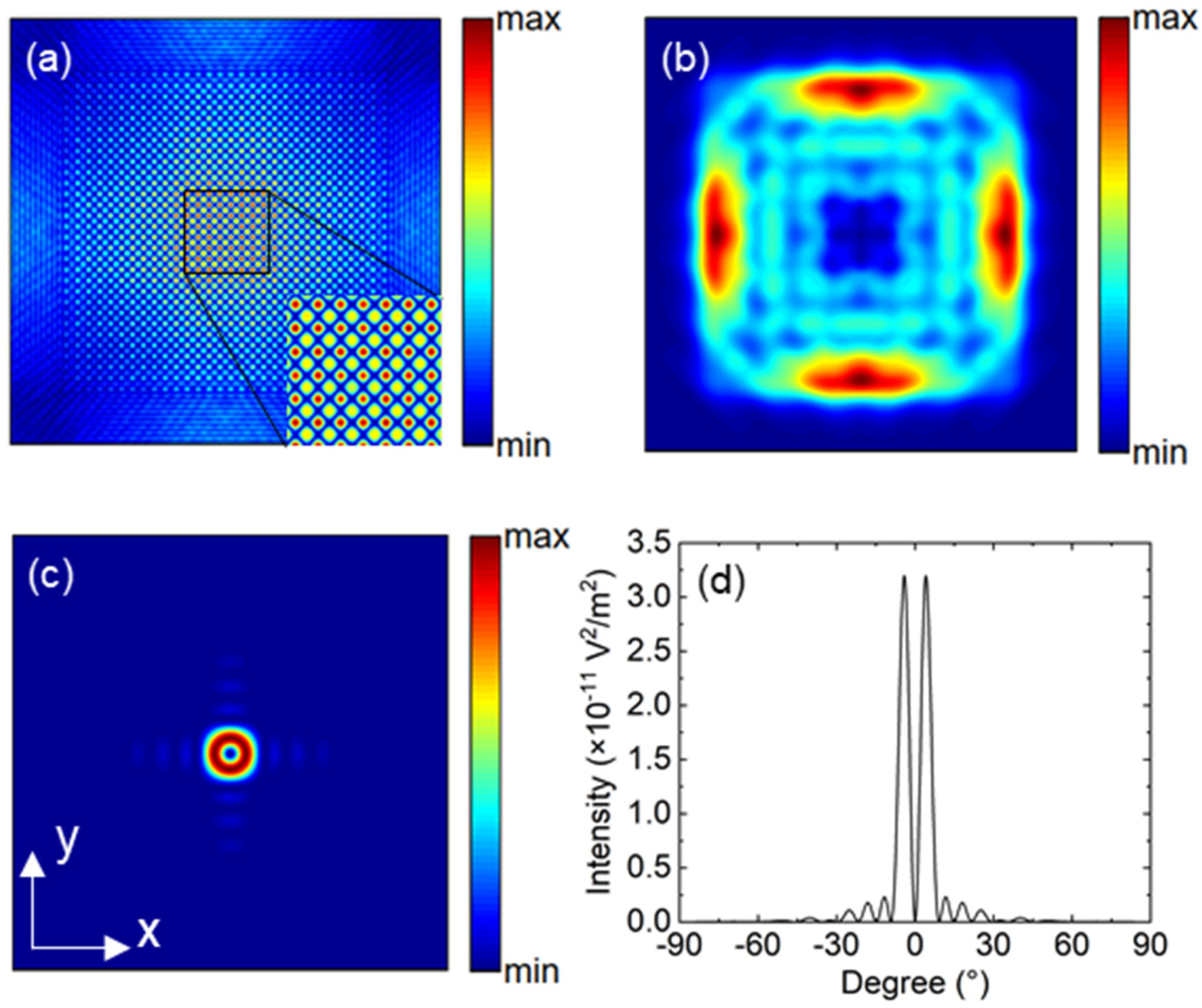
3.1. The Impact of In-Plane PhC Structure

In this part, we adjust the in-plane PhC structure to study its influence on FFP while keeping the other parameters unchanged. The air filling factor, period number, and hole depth are set as 20%, 31, and 160 nm, respectively. The air filling factor is defined as the ratio between the area of air holes and the area of the unit cell. The corresponding FFPs of these structures are obtained by the aforementioned method and will be analyzed from the perspective of symmetry later.
From previous investigations on photonic bands, it was shown that the modulation of light was significantly affected by the optical confinement in the PhC layer [29]. In order to maximize the influence of in-plane PhC structure on the far field, and avoid interference from other complicated factors, we use the PhC slab as the calculation model to obtain the results in Figure 3. In this case, both sides of the PhC layer are air cladded unlike the epi-structure of PCSEL model in Figure 1a. Thereby, the optical confinement in the PhC layer is maximized and so is the coupling coefficient.
In Figure 3, we show the FFP and NFP of PhC slabs with various in-plane structures, including a circle, an isosceles triangle, an isosceles right triangle, and other six structures. They are grouped into two categories, i.e., single-lattice and multiple-lattice structures. The latter can be regarded as several single lattices nested within each other. Since the electric field components determine the final vertical radiation, we calculate their distribution in a single unit cell at the center of slabs. Among single-lattice structures, when the hole-shape of a unit cell is a circle, its electric field distribution exhibits all the same symmetries as the square lattice structure, including rotational symmetry. This leads to negative interference and eventually results in an annular FFP, as mentioned in Figure 2. When its shape changes to an isosceles right triangle, the FFP displays a circular single-lobed spot, which is usually important for a diode laser. This is because the electric field loses the rotational symmetry and then the negative interference effect degrades. When the shape is an isosceles triangle, symmetrical about the x-axis, the FFP displays an elliptical spot with a larger divergence angle in the y-direction than in the x-direction.
Further, we study the FFP corresponding to multiple-lattice PhC structures. This type of PhC structure is more suitable for controlling the in-plane optical loss and vertical radiation factor by adjusting the space between nested lattices or adjusting the shape of holes in each lattice. Thus, some key performances of PCSELs based on them would be flexibly designed, such as modal threshold gain and slope efficiency. Here, we select three double-lattice, two triple-lattice, and one quadruple-lattice PhC structures. The positions of holes are designed to give the PhC structures specific symmetries as described in Table 1. For example, in the case of the triple-lattice structures, the spacing between the holes along both x and y directions are set as half a period. In one of the triple-lattice PhC structures, the offsets of the upper right hole are reduced by 10%, that is, eventually 0.45 times the period along both x and y directions. For the sake of distinction, it is referred to as the deformed triple-lattice structure hereinafter. However, this slight adjustment actually makes the FFP change a lot, from a ring to a circular single lobe.
A square lattice is invariable under eight different symmetry operations, which reflects the symmetry characteristics of the lattice. They are E, C4, C42, C4−1, σx, σy, σd’, σd’’ [30], all of which belong to the C4v point group. Table 1 shows the allowed symmetry operations in different PhC structures. They correspond in turn to the structures in Figure 3. Through seeking the subgroups of C4V point group, all possible combinations of symmetry operations are considered. Among single-lattice structures, the structure with circular air holes has perfect symmetry, allowing all symmetry operations. At the same time, the undeformed triple-lattice one also has perfect symmetry among multiple-lattice structures. Thus, the FFPs arising from them are both annular. The corresponding divergence angles are relatively large, being 13.4° estimated from the 1/e2 width.
The structures named double lattice 1 and double lattice 2 have the second-highest symmetry. They can be kept invariant under both rotational and mirror operations. Their FFPs tend to be double-lobed, with a large divergence angle in the x and y directions. It can be found that the symmetry of their FFP, σd’ and σy, belongs to the allowed symmetry operations of their respective structures. This reveals the consistency among them from the perspective of symmetry.
Further, the other PhC structures have either rotational symmetry or mirror symmetry. Their FFPs are single-lobed and have a lower divergence angle than aforementioned PhC structures. Among all structures, the deformed triple-lattice structure has a completely asymmetric structure and thus obtains a single-lobed far-field spot with low divergence angle as expected. It should be pointed out that the NFPs tend to render the same symmetry characteristic as FFPs, as shown in Figure 3. Thus, their characteristics are not listed independently in Table 1.
In fabrication, holes with special shapes, such as triangles, are more difficult to process than circular shapes. In this way, multi-lattice structures with several circular holes reduce fabrication difficulties compared to single-lattice designs, while achieving the same goal by tuning the hole positions. However, multiple-lattice structures tend to have smaller hole diameters, which is a drawback in the exposure and etching processes, but may be an advantage in the process of retaining air holes during regrowth.

3.2. The Impact of Vertical Epi-Structure

In addition to in-plane PhC structure or hole shape, the air filling factor, hole depth, vertical epi-structure, and even period number also have effects on the FFP, although they are not as direct as the hole shape. As shown in Figure 4, when the air filling factor was reduced from 20% to 13%, the FFP changed from the previous almost-circular single lobe in Figure 4a to the irregular shape with lower central intensity in Figure 4b. This trend is very similar to the structure with circular holes, although its FFP is not a ring as unique as the latter. This illustrates that the decrease in the air filling factor reduces the degree of asymmetry of the structure and then hence the modulation effect on the optical field. Therefore, the central intensity is still affected by the negative interference of the electric field to a certain extent. However, when the hole depth is increased from 160 nm to 320 nm, the central intensity begins to increase, and the spot is transformed towards a better single lobe as shown in Figure 4c, while the air filling factor remained unchanged at 13%.
While all parameters in the PhC layer are the same as those of Figure 4b, including air filling factor, depth, etc., only the air claddings are replaced with an epi-structure as sketched in Figure 1a. The corresponding results are shown in Figure 4d–f. The only variable parameter among them is the period number of PhC, which is 31, 61, and 101, respectively. With the increase in period number, the far field eventually evolves from multi-lobes to an approximately single lobe, which is similar to the result shown in Figure 4b. The introduction of epi-structure lowers the optical confinement factor in the PhC layer and coupling coefficient, and the modulation effect of PhC on electromagnetic field becomes weaker. This is the reason why similar FFP appears at 101 periods, which is much larger than that in the PhC slab. This means that a larger period number in the epi-structure is required if a similar FFP in the PhC slab is wanted.

3.3. The Impact of Period Number

Figure 5 shows the dependence of divergence angle on the size of the PhC cavity in the PhC slab and PCSEL. The periods of PhC in both structures are set as 277 nm. The deformed triple-lattice structure described in Figure 3 is adopted here. After fitting the data, the following inversely proportional relationship was obtained for both curves:
θ = m λ L ,
where θ is the divergence angle expressed in radians, m is the coefficient mainly determined by the in-plane lattice structure whose value is about 1.87 in Figure 5, λ is the resonant wavelength in free space, and L is the size of PhC cavity. Note that the difference of the resonance wavelength corresponding to the two structures leads to two fitting curves that do not overlap. Based on this relationship, it can further control the shape of FFPs to obtain different divergence angles in x and y directions by adjusting the period number of PhC in these two directions, respectively.
This relationship in Equation (1) can be explained through Fraunhofer diffraction theory in the following way: each cell of photonic crystal can be regarded as an independent light emitting unit, and the far field is a result of the coherent superposition of light waves from all units. Since the resonance occurs at the Γ2 point, we assume all emitting units have the same initial phase, so the complex electrical field at the far field is:
E ˜ far ( α , β ) = E ˜ 0 ( α , β ) m = 1 N 1 n = 1 N 2 exp [ i 2 π λ ( ( m 1 ) a cos α + ( n 1 ) a cos β ) ] ,
where E ˜ 0 ( α , β ) is the complex amplitude distribution contributed by a single emitting unit, and we assume its value is the same for all emitting units for simplicity, N1 and N2 are the period number along the x and y directions, a is the period, and α and β are the direction angle of emitting rays along the x and y directions. After simplification, the following formula can be obtained:
E ˜ far ( α , β ) = E ˜ 0 ( α , β ) exp ( i ϕ ) ( sin N 1 δ 1 δ 1 ) ( sin N 2 δ 2 δ 2 ) ,
where:
ϕ = ( N 1 1 ) δ 1 + ( N 2 1 ) δ 2 ,
δ 1 = π λ a cos α ,   δ 2 = π λ a cos β .
Through Equation (3), we deduce that the nearest 1/e times amplitude from the central occurs at directions where:
sin c ( N 1 δ 1 ) sin ( N 1 δ 1 ) N 1 δ 1 = 1 N 1 e , sin c ( N 2 δ 2 ) sin ( N 2 δ 2 ) N 2 δ 2 = 1 N 2 e .
Their values approaches zero when N1 and N2 are large. Then,
N 1 δ 1 = π ,   N 2 δ 2 = π .
Further, assuming their corresponding angles from normal direction, θx and θy, are small, we obtain:
θ x sin θ x = cos α = ± λ N 1 a = ± λ L 1 , θ y sin θ y = cos β = ± λ N 2 a = ± λ L 2
where L1 and L2 are the size of PhC cavity along the x and y directions. Equation (8) is similar to Equation (1) in expression, and implies that coefficient m in Equation (1) should have a value of around 2.
In many applications, a very small beam divergence is necessary. For example, when applied for light detection and ranging and free-space optical communication, laser beams with a divergence angle less than 0.1° or even smaller are needed. According to Equation (1), we deduce that the size of PhC cavity should be larger than 1000 μm at a wavelength of about 940 nm, for example, in order to realize a lens-free application in these fields. For a longer wavelength regime, a larger size is needed.

4. Conclusions

In summary, we have investigated the far-field characteristics of PCSELs using 3D-FDTD simulation. We analyzed the evolution of FFPs from the perspective of group theory and demonstrated that the symmetry of FFPs is consistent with that of the in-plane PhC structure. The symmetry criterion to decrease the divergence angle is increasing the in-plane asymmetry of PhC. Especially, it will result in a circular single lobe when minimum symmetry operations are allowed. Further, we found that a reduction in the thickness of the PhC layer or the introduction of a more complex vertical epi-structure is bad for the formation of a single-lobed FFP because the modulation effect of the PhC on FFP is weakened in this case. However, increasing period number could counteract this negative effect. Moreover, the inverse relationship between the divergence angle and the size of the PhC cavity is provided analytically. When the size of PhC cavity reaches 1000 μm, the beam divergence angle will be as low as 0.1°. We believe that our work will contribute to revealing the mechanism of the influence of PhC geometry on far field and the physical origin of PCSELs’ ultralow divergence angle.

Author Contributions

Conceptualization, Z.W. and C.T.; methodology, Z.W. and C.T.; software, Z.W., P.W. and H.L.; validation, P.W., B.M. and Y.W.; formal analysis, Z.W., B.M. and C.T.; investigation, Z.W. and H.L.; resources, L.W.; data curation, P.W.; writing—original draft preparation, Z.W.; writing—review and editing, B.M. and C.T.; visualization, Z.W.; supervision, L.W; project administration, C.T.; funding acquisition, C.T. All authors have read and agreed to the published version of the manuscript.

Funding

This research was funded by National Key Research and Development Program of China (2018YFB2201000), National Natural Science Foundation of China (61790584, 62025506).

Institutional Review Board Statement

Not applicable.

Informed Consent Statement

Not applicable.

Data Availability Statement

Not applicable.

Conflicts of Interest

The authors declare no conflict of interest.

References

  1. Yoshida, M.; De Zoysa, M.; Ishizaki, K.; Kunishi, W.; Inoue, T.; Izumi, K.; Hatsuda, R.; Noda, S. Photonic-crystal lasers with high-quality narrow-divergence symmetric beams and their application to LiDAR. J. Phys. Photonics 2021, 3, 022006. [Google Scholar] [CrossRef]
  2. Xu, J.; Cheng, Y.; Sugioka, K. Optics for beam shaping in laser processing. In Handbook of Laser Micro- and Nano-Engineering; Springer: Cham, Switzerland, 2021; pp. 527–543. [Google Scholar]
  3. Kaymak, Y.; Rojas-Cessa, R.; Feng, J.; Ansari, N.; Zhou, M. On divergence-angle efficiency of a laser beam in free-space optical communications for high-speed trains. IEEE Trans. Veh. Technol. 2017, 66, 7677. [Google Scholar] [CrossRef]
  4. Wang, Z.; Zhang, J.; Gao, H. Impacts of laser beam divergence on lidar multiple scattering polarization returns from water clouds. J. Quant. Spectrosc. Radiat. Transf. 2021, 268, 107618. [Google Scholar] [CrossRef]
  5. Winterfeldt, M.; Crump, P.; Knigge, S.; Maabdorf, A.; Zeimer, U.; Erbert, G. High beam quality in broad area lasers via suppression of lateral carrier accumulation. IEEE Photonics Technol. Lett. 2015, 27, 1809–1812. [Google Scholar] [CrossRef]
  6. Agrawal, G.P.; Dutta, N.K. Semiconductor Lasers; Kluwer Academic Publishers: Boston, MA, USA, 1993. [Google Scholar]
  7. Martinsson, H.; Vukusic, J.; Grabberr, M.; Michalzik, R.; Jager, R.; Ebeling, K.; Larsson, A. Transverse mode selection in large-area oxide-confined vertical-cavity surface-emitting lasers using a shallow surface relief. IEEE Photonics Technol. Lett. 1999, 11, 1536–1538. [Google Scholar] [CrossRef]
  8. Zhou, D.; Mawst, L.J. High-power single-mode antiresonant reflecting optical waveguide-type vertical-cavity surface-emitting lasers. IEEE J. Quantum Electron. 2002, 38, 1599–1606. [Google Scholar] [CrossRef] [Green Version]
  9. Bardinal, V.; Camps, T.; Reig, B.; Barat, D.; Daran, E.; Doucet, J.B. Collective micro-optics technologies for VCSEL photonic integration. Adv. Opt. Technol. 2013, 2011, 609643. [Google Scholar] [CrossRef] [Green Version]
  10. Chang, Y.-C.; Shin, M.C.; Phare, C.T.; Miller, S.A.; Shim, E.; Lipson, M. 2D beam steerer based on metalens on silicon photonics. Opt. Express 2021, 29, 854. [Google Scholar] [CrossRef]
  11. Engelberg, J.; Levy, U. The advantages of metalenses over diffractive lenses. Nat. Commun. 2020, 11, 1991. [Google Scholar] [CrossRef] [Green Version]
  12. Hirose, K.; Liang, Y.; Kurosaka, Y.; Watanabe, A.; Sugiyama, T.; Noda, S. Watt-class high-power, high-beam-quality photonic-crystal lasers. Nat. Photonics 2014, 8, 406–411. [Google Scholar] [CrossRef]
  13. Ishizaki, K.; De Zoysa, M.; Noda, S. Progress in photonic-crystal surface-emitting lasers. Photonics 2019, 6, 96. [Google Scholar] [CrossRef] [Green Version]
  14. Yoshida, M.; De Zoysa, M.; Ishizaki, K.; Tanaka, Y.; Kawasaki, M.; Hatsuda, R.; Song, B.; Gelleta, J.; Noda, S. Double-lattice photonic-crystal resonators enabling high-brightness semiconductor lasers with symmetric narrow-divergence beams. Nat. Mater. 2019, 18, 121–128. [Google Scholar] [CrossRef] [PubMed]
  15. Zhou, W.; Liu, S.-C.; Ge, X.; Zhao, D.; Yang, H.; Reuterskiold-Hedlund, C.; Hammar, M. On-chip photonic crystal surface-emitting membrane lasers. IEEE J. Sel. Top. Quantum Electron. 2019, 25, 4900211. [Google Scholar] [CrossRef]
  16. Lu, H.-Y.; Tian, S.-C.; Tong, C.-Z.; Wang, L.-J.; Rong, J.-M.; Liu, C.-Y.; Wang, H.; Shu, S.; Wang, L.-J. Extracting more light for vertical emission: High power continuous wave operation of 1.3-μm quantum-dot photonic-crystal surface-emitting laser based on a flat band. Light Sci. Appl. 2019, 8, 108. [Google Scholar] [CrossRef] [PubMed] [Green Version]
  17. Li, G.; Sarma, J.; Taylor, R.J.E.; Childs, D.T.D.; Hogg, R.A. Modeling and Device Simulation of Photonic Crystal Surface Emitting Lasers Based on Modal Index Analysis. IEEE J. Sel. Top. Quantum Electron. 2019, 25, 1–9. [Google Scholar] [CrossRef] [Green Version]
  18. Chen, L.-R.; Hong, K.-B.; Huang, K.-C.; Yen, H.-T.; Lu, T.-C. Improvement of output efficiency of p-face up photonic-crystal surface-emitting lasers. Opt. Express 2021, 29, 11293–11300. [Google Scholar] [CrossRef]
  19. Katsuno, S.; Yoshida, M.; Izumi, K.; Inoue, T.; Ishizaki, K.; De Zoysa, M.; Hatsuda, R.; Gelleta, J.; Enoki, K.; Noda, S. 29-W continuous-wave operation of photonic-crystal surface-emitting laser (PCSEL). In Proceedings of the 27th International Semiconductor Laser Conference (ISLC), Matsue, Japan, 16–19 October 2021. [Google Scholar]
  20. Morita, R.; Inoue, T.; De Zoysa, M.; Ishizaki, K.; Noda, S. Photonic-crystal lasers with two-dimensionally arranged gain and loss sections for high-peak-power short-pulse operation. Nat. Photonics 2021, 15, 311–318. [Google Scholar] [CrossRef]
  21. Inoue, T.; Yoshida, M.; Gelleta, J.; Izumi, K.; Yoshida, K.; Ishizaki, K.; De Zoysa, M.; Noda, S. General recipe to realize photonic-crystal surface-emitting lasers with 100-W-to-1-kW single-mode operation. Nat. Commun. 2022, 13, 3262. [Google Scholar] [CrossRef]
  22. Eiji, M.; Kyosuke, S.; Takayuki, O.; Wataru, K.; Dai, O.; Susumu, N. Lasers producing tailored beams. Nature 2006, 441, 946. [Google Scholar]
  23. Liang, Y.; Peng, C.; Sakai, K.; Iwahashi, S.; Noda, S. Three-dimensional coupled-wave analysis for square-lattice photonic crystal surface emitting lasers with transverse-electric polarization: Finite-size effects. Opt. Express 2012, 20, 15945–15961. [Google Scholar] [CrossRef]
  24. Yokoyama, M.; Noda, S. Finite-difference time-domain simulation of two dimensional photonic crystal surface-emitting laser. Opt. Express 2005, 13, 2869. [Google Scholar] [CrossRef] [PubMed]
  25. Wang, Z.; Liang, Y.; Beck, M.; Scalari, G.; Faist, J. Topological charge of finite-size photonic crystal modes. Phys. Rev. B 2020, 102, 045122. [Google Scholar] [CrossRef]
  26. Yokoyama, M.; Noda, S. Finite-difference time-domain simulation of two-dimensional photonic crystal surface-emitting laser having a square-lattice slab structure. IEICE Transanctions Electron. 2004, 87, 386–392. [Google Scholar]
  27. Bian, Z.; Rae, K.J.; McKenzie, A.F.; King, B.C.; Babazadeh, N.; Li, G.; Orchard, J.R.; Gerrard, N.D.; Thoms, S.; MacLaren, D.A.; et al. 1.5 μm epitaxially regrown photonic crystal surface emitting laser diode. IEEE Photonics Technol. Lett. 2020, 32, 1531–1534. [Google Scholar] [CrossRef]
  28. Itoh, Y.; Kono, N.; Fujiwara, N.; Yagi, H.; Katsuyama, T.; Kitamura, T.; Fujii, K.; Ekawa, M.; Shoji, H.; Inoue, T.; et al. Continous-wave lasing operation of 1.3-μm wavelength InP-based photonic crystal surface-emitting lasers using MOVPE regrowth. Opt. Express 2020, 28, 35483–35489. [Google Scholar] [CrossRef]
  29. Sakai, K.; Miyai, E.; Sakaguchi, T.; Ohnishi, D.; Okano, T.; Noda, S. Lasing band-edge identification for a surface-emitting photonic crystal laser. IEEE J. Sel. Areas Commun. 2005, 23, 1335–1340. [Google Scholar] [CrossRef]
  30. Sakoda, K. Optical Properties of Photonic Crystals; Springer: Berlin, Germany, 2004. [Google Scholar]
Figure 1. (a) Schematic of the photonic-crystal surface-emitting laser (PCSEL) model adopted in the simulation. The orange layer represents active layer, below which is the photonic crystal (PhC) layer. The top and bottom layers are cladding layers. The translucent blue planes represent field monitors. The red box represents simulation region. The yellow arrow represents light emission direction. (b) The typical photonic band of the square-lattice PCSEL near Γ2 point. Point A is the band edge where PCSELs commonly work at.
Applsci 12 10581 g001
Figure 2. The simulation results of the square-lattice PCSEL with circular air holes. (a) Magnetic field distribution inside the PhC layer. (b) Near-field pattern (NFP) and (c) far-field pattern (FFP) of the PCSEL. (d) The intensity profile at the center of (c) along x-direction.
Applsci 12 10581 g002
Figure 3. The schematic of various in-plane PhC structures and their corresponding electric field, FFP, and NFP. The period number of PhC is 31.
Applsci 12 10581 g003
Figure 4. The FFP and NFP of devices with right isosceles triangular air holes. The former three groups are PhC slab clad by air, with the same period numbers of 31, but with various air filling factors and hole depths of (a) 20%, 160 nm, (b) 13%, 160 nm, (c) 13%, 320 nm, respectively. The latter three groups are PCSELs clad by dielectric layers, with the same air filling factor of 13% and hole depth of 160 nm, but various period numbers of (d) 31, (e) 61, (f) 101, respectively.
Applsci 12 10581 g004
Figure 5. Divergence angle versus the size of PhC cavity for PhC slab and PCSEL, respectively. The air filling factor and hole depth are kept as 20% and 160 nm.
Applsci 12 10581 g005
Table 1. The symmetry characteristics and far-field performance of various PhC structures.
PhC StructureSymmetry of PhCFFPSymmetry of FFPDivergence Angle (o)
EC4C42C4−1σxσyσdσd’’xy
Single latticeCircle√ *AnnularC4v13.413.4
Isosceles
triangle
Elliptical
single-lobed
E, σy11.012.1
Isosceles right
triangle
Circular
single-lobed
E, σd11.011.0
Multiple latticeDouble lattice 1 Double-lobedE, σd13.313.3
Double lattice 2 Double-lobedE, σy14.314.0
Double lattice 3 Circular
single-lobed
E, C4210.310.3
Undeformed
triple lattice
AnnularC4v13.413.4
Deformed
triple lattice
Circular
single-lobed
E10.810.6
Quadruple lattice Circular
single-lobed
E, C4211.311.3
* Symbol √ means that the corresponding symmetry is satisfied.
Publisher’s Note: MDPI stays neutral with regard to jurisdictional claims in published maps and institutional affiliations.

