
Simulation of Optical Nano-Manipulation with Metallic Single and Dual Probe Irradiated by Polarized Near-Field Laser


Abstract
:1. Introduction
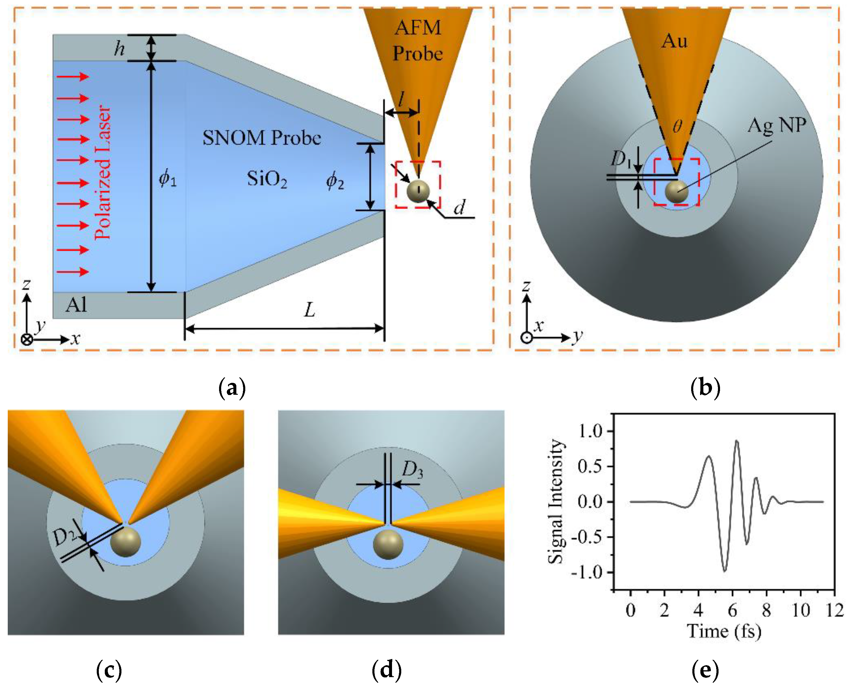
2. Methods
3. Results and Discussion
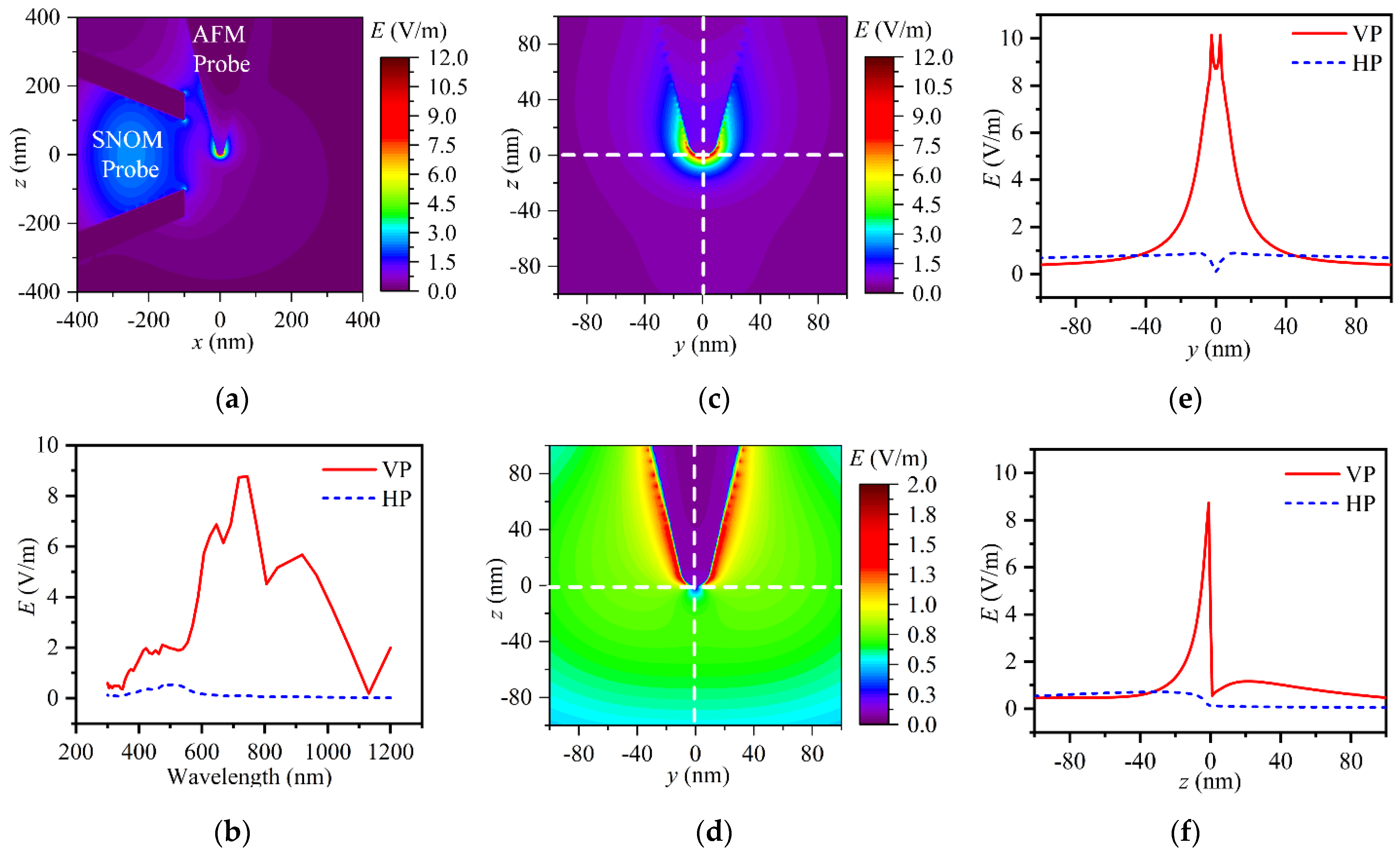
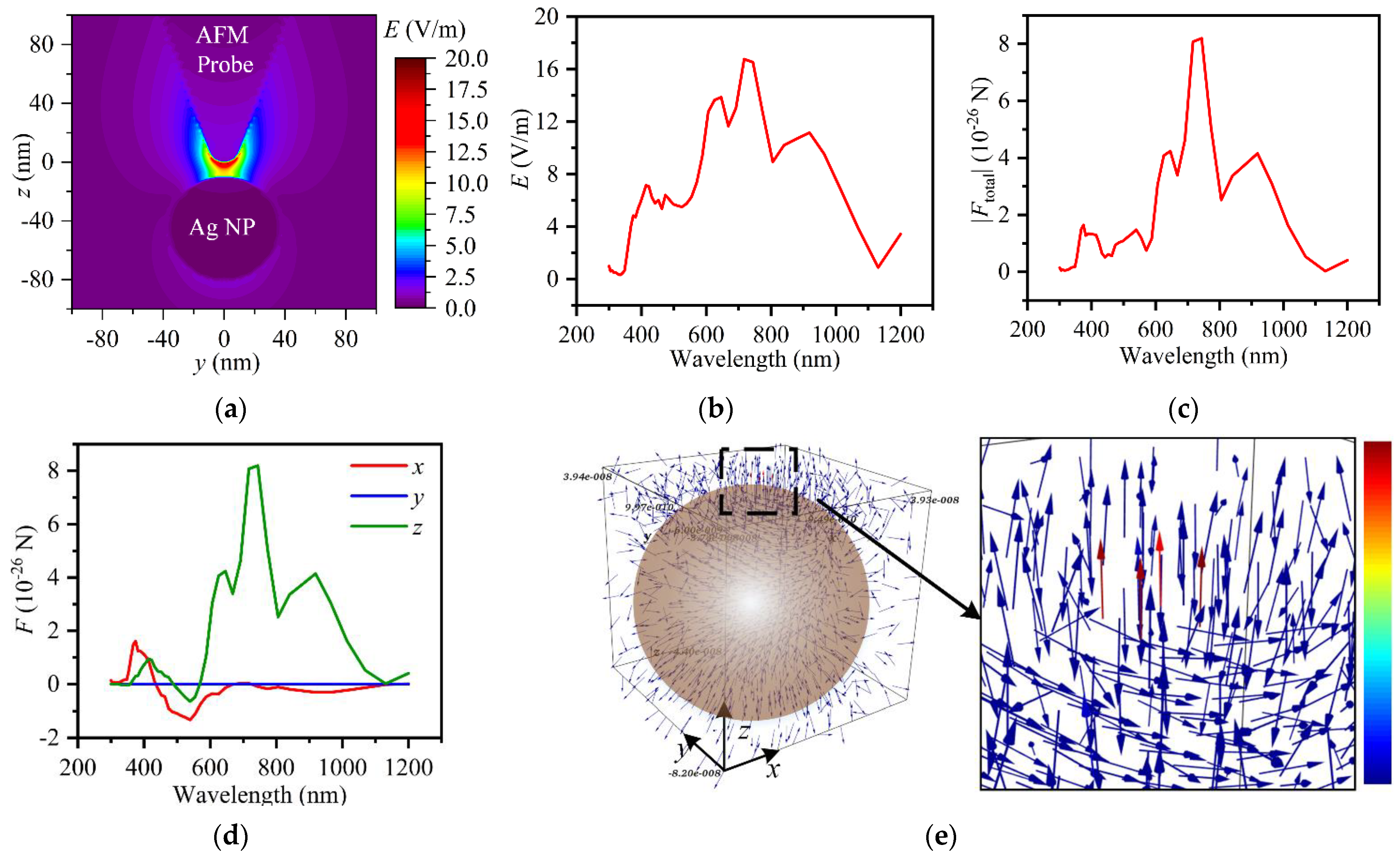
3.1. Distribution of Electric Field around Tip without NP
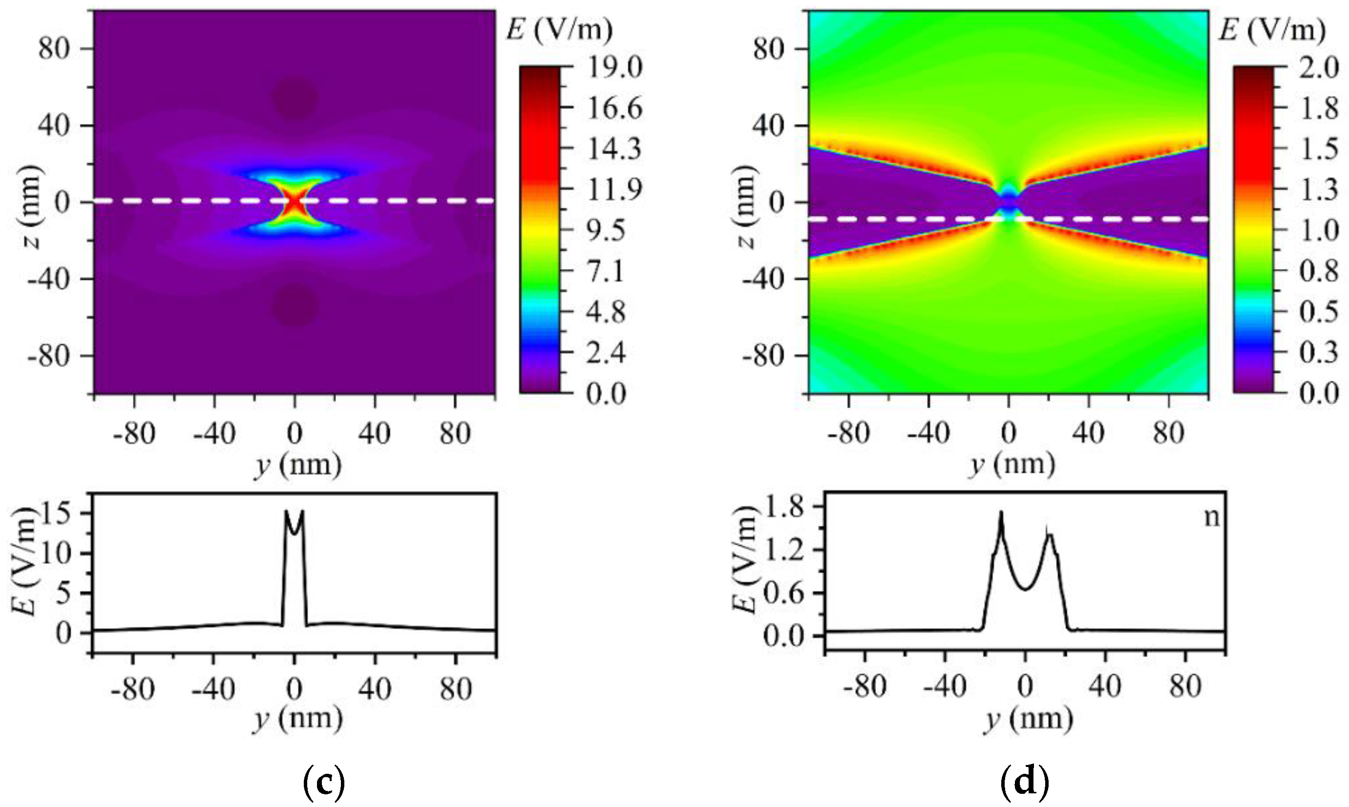
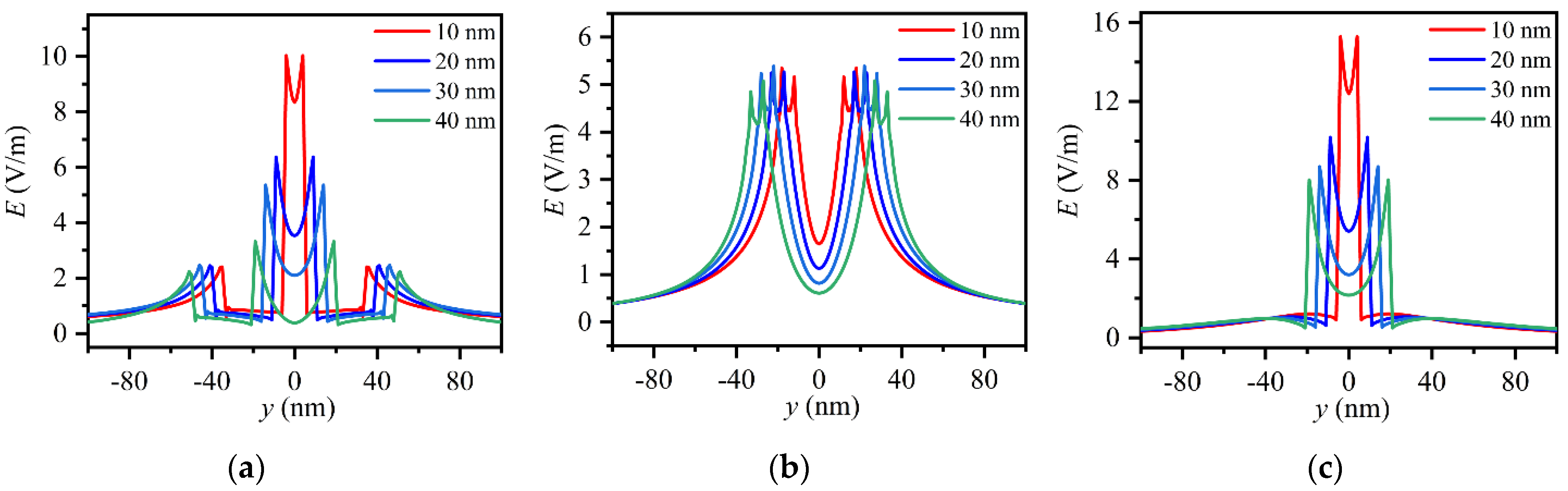
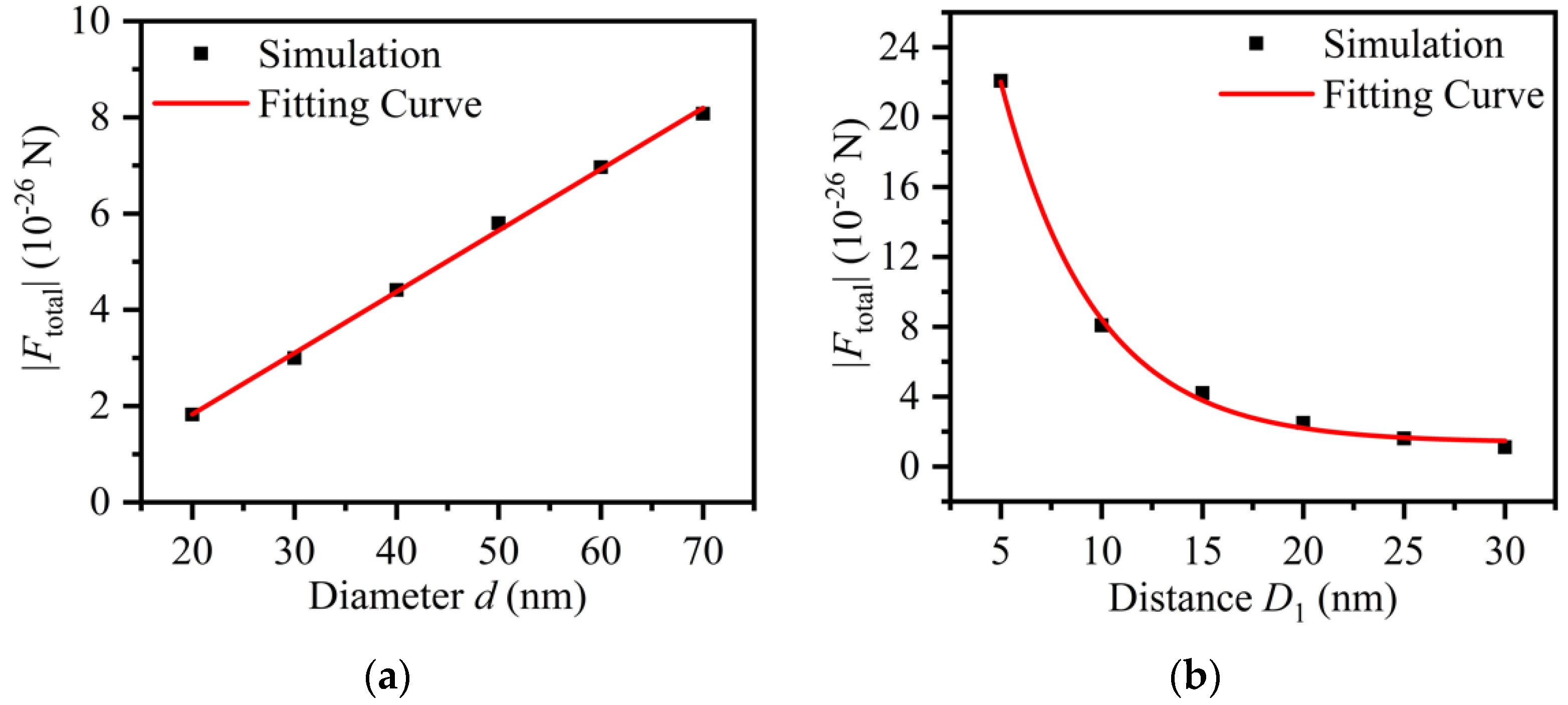
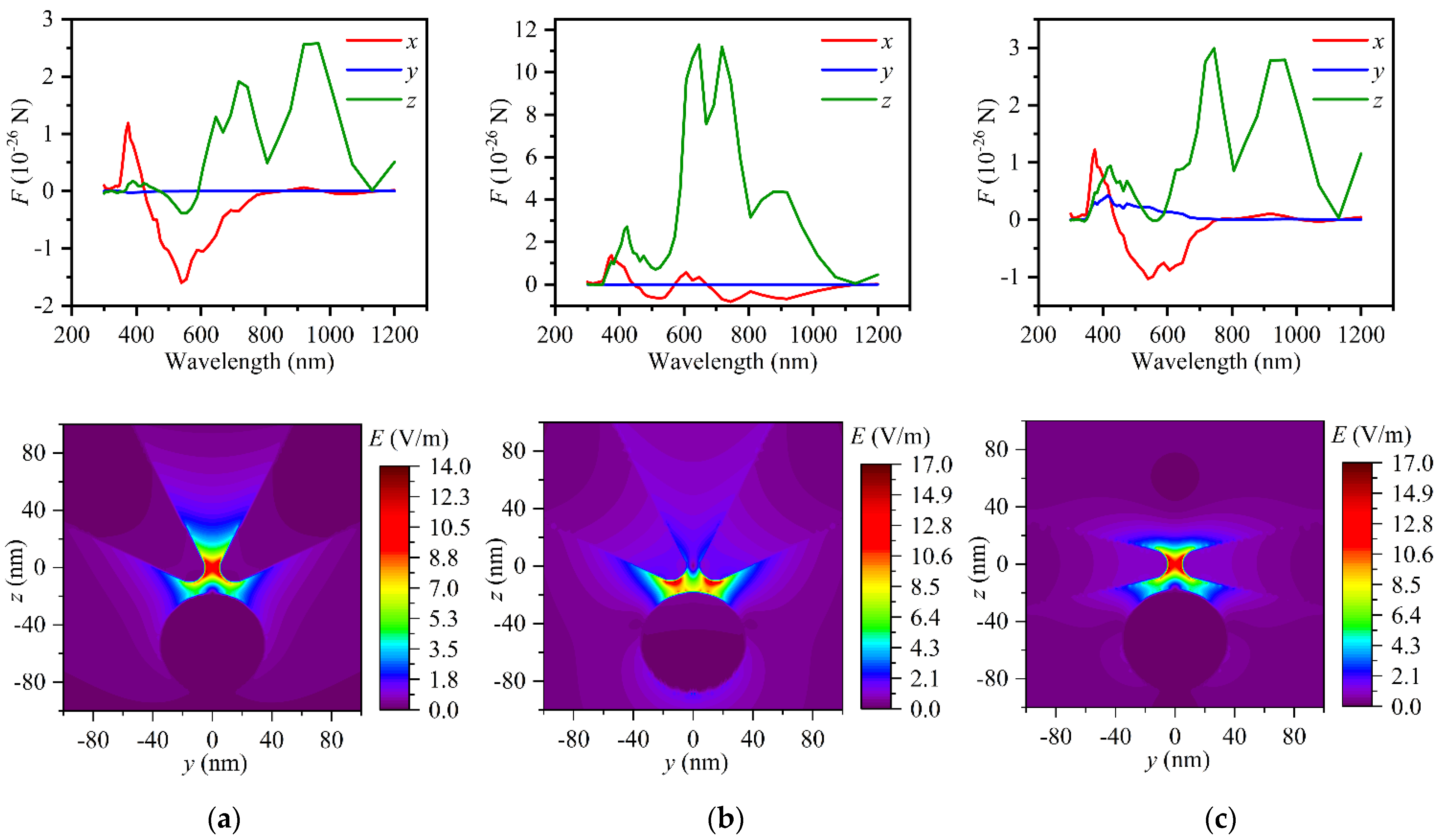
3.2. Trapping Force of an NP in Enhanced Near-Field
4. Conclusions
Supplementary Materials
Author Contributions
Funding
Institutional Review Board Statement
Informed Consent Statement
Data Availability Statement
Acknowledgments
Conflicts of Interest
References
- Eigler, D.M.; Schweizer, E.K. Positioning single atoms with a scanning tunnelling microscope. Nature 1990, 344, 524–526. [Google Scholar] [CrossRef]
- Jiang, C.; Lu, H.; Zhang, H.; Shen, Y.; Lu, Y. Recent advances on in situ SEM mechanical and electrical characterization of low-dimensional nanomaterials. Scanning 2017, 2017, 1–11. [Google Scholar]
- Ono, M.; Kuramochi, E.; Zhang, G.; Sumikura, H.; Harada, Y.; Cox, D.; Notomi, M. Nanowire-nanoantenna coupled system fabricated by nanomanipulation. Opt. Express 2016, 24, 8647–8659. [Google Scholar] [CrossRef]
- Ratchford, D.; Shafiei, F.; Kim, S.; Gray, S.K.; Li, X. Manipulating coupling between a single semiconductor quantum dot and single gold nanoparticle. Nano Lett. 2011, 11, 1049–1054. [Google Scholar] [CrossRef]
- Wang, H.; Shi, Q.; Nakajima, M.; Takeuchi, M.; Chen, T.; Di, P.; Huang, Q.; Fukuda, T. Rail-guided multi-robot system for 3D cellular hydrogel assembly with coordinated nanomanipulation. Int. J. Adv. Robot. Syst. 2014, 11, 1–9. [Google Scholar] [CrossRef]
- Vasić, B.; Matković, A.; Gajić, R.; Stanković, I. Wear properties of graphene edges probed by atomic force microscopy based lateral manipulation. Carbon 2016, 107, 723–732. [Google Scholar] [CrossRef]
- Shi, C.; Luu, D.K.; Yang, Q.; Liu, J.; Chen, J.; Ru, C.; Xie, S.; Luo, J.; Ge, J.; Sun, Y. Recent advances in nanorobotic manipulation inside scanning electron microscopes. Microsyst. Nanoeng. 2016, 2, 1–16. [Google Scholar] [CrossRef] [Green Version]
- Cao, C.; Zhang, Z.; Amirmaleki, M.; Tam, J.; Dou, W.; Filleter, T.; Sun, Y. Local strain mapping of GO nanosheets under in situ TEM tensile testing. Appl. Mater. Today 2019, 14, 102–107. [Google Scholar] [CrossRef]
- Van der Lit, J.; Jacobse, P.H.; Vanmaekelbergh, D.; Swart, I. Bending and buckling of narrow armchair graphene nanoribbons via STM manipulation. New J. Phys. 2015, 17, 053013. [Google Scholar] [CrossRef]
- Kim, S.; Ratchford, D.C.; Li, X. Atomic force microscope nanomanipulation with simultaneous visual guidance. ACS Nano 2009, 3, 2989–2994. [Google Scholar] [CrossRef]
- Lu, X.; Liu, J.; Ding, Y.; Yang, L.; Yang, Z.; Wang, Y. Simulation and fabrication of carbon nanotube–nanoparticle interconnected structures. Mech. Sci. 2021, 12, 451–459. [Google Scholar] [CrossRef]
- Xie, H.; Haliyo, D.S.; Régnier, S. A versatile atomic force microscope for three-dimensional nanomanipulation and nanoassembly. Nanotechnology 2009, 20, 215301. [Google Scholar] [CrossRef] [Green Version]
- Zimmermann, S.; Tiemerding, T.; Fatikow, S. Automated robotic manipulation of individual colloidal particles using vision-based control. IEEE/ASME Trans. Mechatron. 2014, 20, 2031–2038. [Google Scholar] [CrossRef]
- Chen, H.; Zhang, X.L.; Zhang, Y.Y.; Wang, D.; Bao, D.L.; Que, Y.; Xiao, W.; Du, S.; Ouyang, M.; Pantelides, S.T.; et al. Atomically precise, custom-design origami graphene nanostructures. Science 2019, 365, 1036–1040. [Google Scholar] [CrossRef] [Green Version]
- Moreno-Moreno, M.; Ares, P.; Moreno, C.; Zamora, F.; Gomez-Navarro, C.; Gomez-Herrero, J. AFM manipulation of gold nanowires to build electrical circuits. Nano Lett. 2019, 19, 5459–5468. [Google Scholar] [CrossRef] [Green Version]
- Ashkin, A.; Dziedzic, J.M.; Bjorkholm, J.E.; Chu, S. Observation of a single-beam gradient force optical trap for dielectric particles. Opt. Lett. 1986, 11, 288–290. [Google Scholar] [CrossRef] [Green Version]
- Yan, Z.; Jureller, J.E.; Sweet, J.; Guffey, M.J.; Pelton, M.; Scherer, N.F. Three-dimensional optical trapping and manipulation of single silver nanowires. Nano Lett. 2012, 12, 5155–5161. [Google Scholar] [CrossRef]
- Jauffred, L.; Taheri, S.M.R.; Schmitt, R.; Linke, H.; Oddershede, L.B. Optical trapping of gold nanoparticles in air. Nano Lett. 2015, 15, 4713–4719. [Google Scholar] [CrossRef] [PubMed] [Green Version]
- Li, Y.; Guo, Z.; Qu, S. Living cell manipulation in a microfluidic device by femtosecond optical tweezers. Opt. Lasers Eng. 2014, 55, 150–154. [Google Scholar] [CrossRef]
- Eriksson, E.; Sott, K.; Lundqvist, F.; Sveningsson, M.; Scrimgeour, J.; Hanstorp, D.; Goksör, M.; Granéli, A. A microfluidic device for reversible environmental changes around single cells using optical tweezers for cell selection and positioning. Lab A Chip 2010, 10, 617–625. [Google Scholar] [CrossRef]
- Mandal, S.; Serey, X.; Erickson, D. Nanomanipulation using silicon photonic crystal resonators. Nano Lett. 2010, 10, 99–104. [Google Scholar] [CrossRef] [PubMed]
- Zhang, W.; Huang, L.; Santschi, C.; Martin, O.J. Trapping and sensing 10 nm metal nanoparticles using plasmonic dipole antennas. Nano Lett. 2010, 10, 1006–1011. [Google Scholar] [CrossRef] [PubMed] [Green Version]
- Kotnala, A.; Gordon, R. Quantification of high-efficiency trapping of nanoparticles in a double nanohole optical tweezer. Nano Lett. 2014, 14, 853–856. [Google Scholar] [CrossRef] [PubMed]
- Keyi, W.; Zhen, J.; Wenhao, H. The possibility of trapping and manipulating a nanometer scale particle by the SNOM tip. Opt. Commun. 1998, 149, 38–42. [Google Scholar] [CrossRef]
- Berthelot, J.; Aćimović, S.S.; Juan, M.L.; Kreuzer, M.P.; Renger, J.; Quidant, R. Three-dimensional manipulation with scanning near-field optical nanotweezers. Nat. Nanotechnol. 2014, 9, 295–299. [Google Scholar] [CrossRef] [PubMed]
- Liu, B.; Yang, L.; Wang, Y. Optical trapping force combining an optical fiber probe and an AFM metallic probe. Opt. Express 2011, 19, 3703–3714. [Google Scholar] [CrossRef]
- Liu, B.; Yang, L.; Wang, Y. Simulation of near-field optical manipulator using the combination of a near-field scanning optical microscope probe and an atomic force microscope metallic probe. J. Appl. Phys. 2011, 109, 104317. [Google Scholar] [CrossRef]
- Cui, J.; Yang, L.; Wang, Y.; Mei, X.; Wang, W.; Hou, C. Nanospot soldering polystyrene nanoparticles with an optical fiber probe laser irradiating a metallic AFM probe based on the near-field enhancement effect. ACS Appl. Mater. Interfaces 2015, 7, 2294–2300. [Google Scholar] [CrossRef] [PubMed]
- Liu, B.; Yang, L.; Wang, Y. Near-Field Optical Tweezers Based on NSOM and AFM Probes. Integr. Ferroelectr. 2012, 136, 59–65. [Google Scholar] [CrossRef]

Publisher’s Note: MDPI stays neutral with regard to jurisdictional claims in published maps and institutional affiliations. |
© 2022 by the authors. Licensee MDPI, Basel, Switzerland. This article is an open access article distributed under the terms and conditions of the Creative Commons Attribution (CC BY) license (https://creativecommons.org/licenses/by/4.0/).
Share and Cite
Wang, G.; Ding, Y.; Long, H.; Guan, Y.; Lu, X.; Wang, Y.; Yang, L. Simulation of Optical Nano-Manipulation with Metallic Single and Dual Probe Irradiated by Polarized Near-Field Laser. Appl. Sci. 2022, 12, 815. https://doi.org/10.3390/app12020815
Wang G, Ding Y, Long H, Guan Y, Lu X, Wang Y, Yang L. Simulation of Optical Nano-Manipulation with Metallic Single and Dual Probe Irradiated by Polarized Near-Field Laser. Applied Sciences. 2022; 12(2):815. https://doi.org/10.3390/app12020815
Chicago/Turabian StyleWang, Genwang, Ye Ding, Haotian Long, Yanchao Guan, Xiwen Lu, Yang Wang, and Lijun Yang. 2022. "Simulation of Optical Nano-Manipulation with Metallic Single and Dual Probe Irradiated by Polarized Near-Field Laser" Applied Sciences 12, no. 2: 815. https://doi.org/10.3390/app12020815
APA StyleWang, G., Ding, Y., Long, H., Guan, Y., Lu, X., Wang, Y., & Yang, L. (2022). Simulation of Optical Nano-Manipulation with Metallic Single and Dual Probe Irradiated by Polarized Near-Field Laser. Applied Sciences, 12(2), 815. https://doi.org/10.3390/app12020815