Article

Development of 1.3 GHz Medium-β (β = 0.634) Disk-Loaded Deflecting Cavity for 150 keV Electron Beam

State Key Laboratory of Nuclear Physics and Technology, Peking University, Beijing 100871, China
*
Author to whom correspondence should be addressed.
Appl. Sci. 2022, 12(18), 9243; https://doi.org/10.3390/app12189243
Submission received: 23 July 2022 / Revised: 6 September 2022 / Accepted: 13 September 2022 / Published: 15 September 2022
(This article belongs to the Special Issue Nuclear Techniques and Material Analysis)

Abstract

:
A miniaturized 150 kV DC photocathode gun is developed at Peking University to generate electron beam which can be manipulated in temporal and spatial distribution as requirements freely. To measure the bunch length which is an important temporal parameter of the low energy electron beam from the DC photocathode gun, a 1.3 GHz medium-β disk-loaded deflecting cavity is adopted. In this paper we present the design of the deflecting cavity which involves the microwave design including the geometry optimization and the separation of the orthogonal dipole modes as well as the power coupling, the mechanical design including the determination of the cavity wall thickness and the tuning as well as brazing structure, and the thermodynamic analysis. Particle tracking simulation shows that the best resolution of 190 fs can be achieved for the 150 keV electron beam by using the deflecting cavity. Its fabrication is completed and the RF measurements are carried out with a vector network analyzer. It is shown the measured values of the RF physical parameters are in good agreement with the simulation design ones.

1. Introduction

The 150 kV DC photocathode gun at Peking University will be used as the source to produce electron beams which can be manipulated in temporal and spatial distribution as requirements freely. The measurements of the electron beam bunch length are proposed. Till now, many well-known measurement methods have been developed including electro-optical sampling [1], streak camera [2], auto-correlation method [3], harmonic analysis [4], zero-phase cross [5], ponderomotive scattering [6], etc. In recent years, deflecting cavities have been widely used for bunch length measurement because there is no limitation of the bunch charge and beam energy. Its principle is that the head and tail of the bunch experience opposite transverse deflecting force through the cavity and then the bunch drifts a certain length producing a spot on the YAG screen, the size of the spot is linearly related to the bunch length [7]. Generally, a higher operation frequency can provide a higher measurement resolution, and increasing the number of cells could enhance the deflecting ability of the cavity with the same input power. To diagnose electron beams with energy of several MeV or even GeV, many laboratories developed different deflecting cavities. Two 117-cell disk-loaded X-band deflectors at LCLS [8], two 1.7 m disk-loaded C-band deflectors at Spring-8 [9], a 96-cell and a 120-cell disk-loaded X-band deflectors at SwissFEL [10], a 47-cell disk-loaded X-band deflector at SINAP [11] were used for GeV electron beam diagnosis. A 1.3 GHz single-cell deflecting cavity with protrusions inside at Cornell University [12], a 2.9985 GHz 9-cell deflecting cavity at Daresbury Laboratory [13], a 2.856 GHz 2-cell rectangular deflecting cavity at Waseda University [14], a 2.856 GHz 7-cell disk-loaded deflecting cavity at Tsinghua University [15], a 2.856 GHz single-cell rectangular deflecting cavity at KAERI [16] were developed for electron beam diagnosis with energy of several MeV. The bunch length measurements of the electron beam with energy lower than 1 MeV are also being developed, Eindhoven University of Technology developed a 2.9995 GHz reentrant cavity to measure the length of 95 keV electron beams in their UED experiment [17]. KEK fabricated a 2.6 GHz single-cell deflecting cavity similar to a rectangular cavity at compact ERL injector, to measure the electron beam from their 500 kV high voltage photoemission DC gun [18]. Different from the ones just mentioned, a 1.3 GHz medium- β disk-loaded standing-wave cylindrical deflecting cavity is adopted, since the fabrication of a cylindrical cavity is more convenient and much easier than that of a rectangular cavity and a reentrant cavity.
In this paper, the deflecting cavity is fabricated and tested, which is also installed in the beamline eventually. Firstly, the design of the 1.3 GHz standing-wave normal-conducting disk-loaded deflecting cavity including the microwave design is presented. In addition, the beam dynamics simulation for the deflecting cavity is taken. Next, the mechanical design and thermodynamic analysis is carried out. Finally, after fabricating the RF measurement results is presented including the resonant frequency, the intrinsic quality factor ( Q 0 ), external quality factor ( Q e ), and field distribution.

2. Deflecting Cavity Design

The bunch length can be calculated in the deflecting cavity measurement by the following equation:
σ t = β 2 W ω q V d e f D σ y 2 σ y , 0 2
and the resolution formula is
Δ t = β 2 W σ y , 0 ω q V d e f D
where β is the velocity of electron divided by light velocity, W is the total energy of the electron beam including kinetic energy and rest energy, ω is the angle frequency of the microwave, V d e f is the effective deflecting voltage, D is the drift distance, σ y , 0 and σ y are the vertical RMS bunch size at the screen with the deflecting cavity off and on, respectively.
To achieve the resolution of less than 200 fs for the 150 keV electron beam, numerical analysis shows that the 1.3 GHz cavity is expected to provide a deflecting voltage of 50 kV while assuming σ y , 0 is 0.1 mm and D is about 0.6 m.

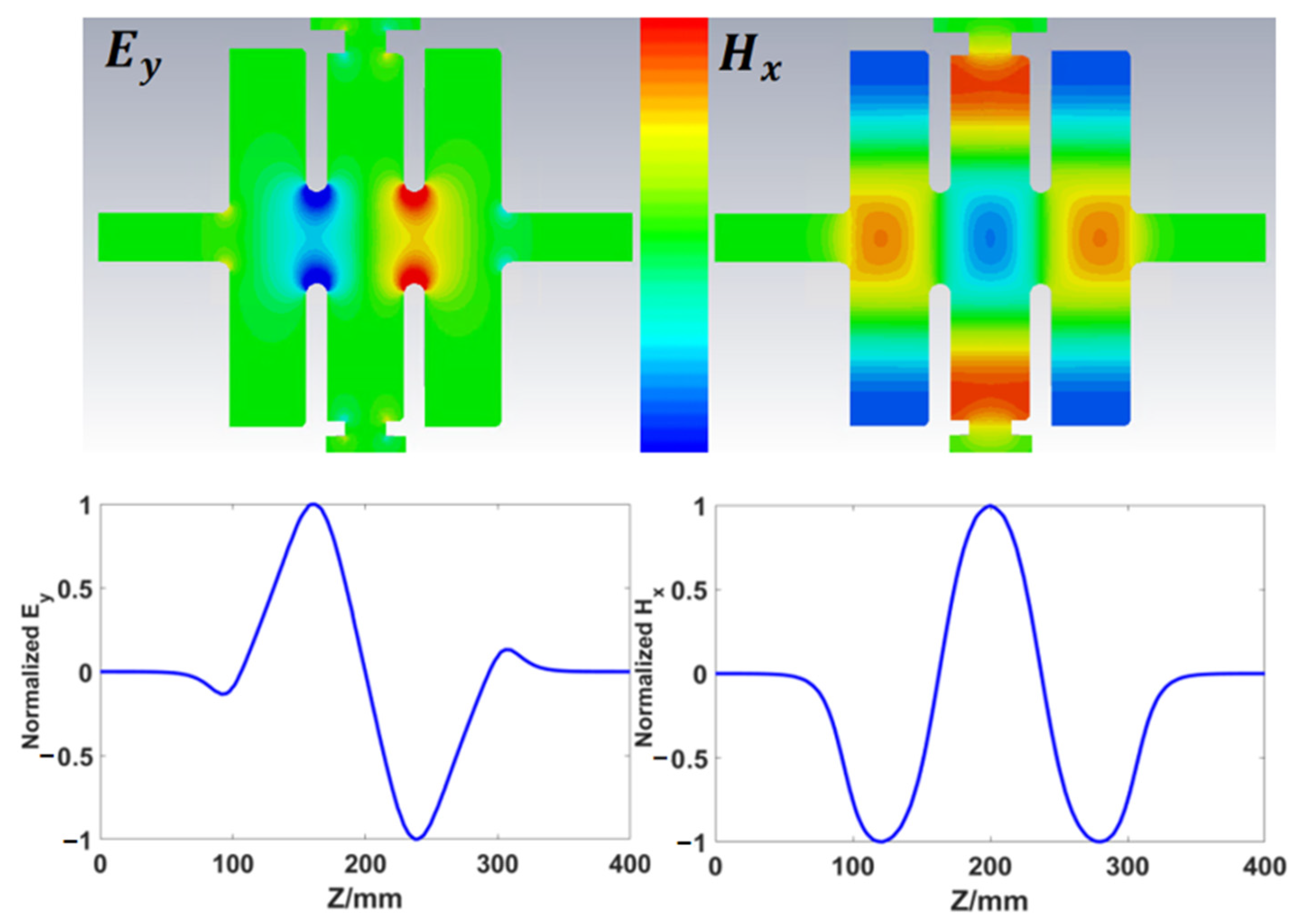
2.1. Microwave Design and Particle Tracking

Microwave design is carried out in CST [19], which includes geometry optimization, mode separation and power coupling design.
The normal-conducting standing-wave deflecting cavity is designed based on circular waveguide, and its working mode is TM 110 . Benefiting from the good design of the 150 kV DC structure, the electron is accelerated relatively uniformly from the photocathode. The energy spread is low enough to neglect at low bunch charge. Therefore, the average beta of the electron beam is considered during the cavity geometry optimization. The single-cell length of the standing-wave deflecting cavity is
l = β g λ / 2
where β g is the geometric beta of the deflecting structure which is nearly the same as the electron beam beta β , λ is the wavelength of the electromagnetic field. As the β of the electron beam from the DC photocathode gun is 0.634, if the β g of deflecting cavity is equal to β , the TM110 transverse shunt impedance R of a pure copper pillbox cavity is about 0.4 MΩ. In this paper, the polarization direction of the working mode is chosen along y-axis, so the definition of transverse shunt impedance is
R =   V d e f 2 P = β 2 |   E z ( x = 0 , y = y 0 ) e j k z β d z | 2 ω U ( k y 0 ) 2
where the integration path takes off-axis (x = 0, y   =   y 0 ), P is the power dissipated in the cavity walls, k is wave-number of the microwave.
To provide higher deflecting voltage with same input power, a 3-cell cavity is finally adopted. The two-dimensional diagram of the deflecting cavity is shown in Figure 1.
The key geometric parameters are optimized. Cavity radii b m and b e are optimized for the goal resonant frequency and better field flatness. The cell length l comprising disk thickness t and the length d is optimized to acquire the value of the shunt impedance R as high as possible. Considering that obvious mechanical deformation could occur during fabrication if t is too small, and a large t is not beneficial to R , a compromised resolution with t of 16 mm is made. As the cavity deflects electron beam with medium- β , the cell length l is calculated in detail in the following.
In this paper, three structures with different cavity length are optimized. The simulations start from simple structures of which the three cells have equal length. The first structure is that each cell length is as Equations (2) and (3) with β g of 0.634. Simulation shows the R acquire its maximum value at β   of 0.72. To enable the   R acquire its maximum value at β of 0.634, the simulations show that β g should be equal to 0.551 which is called as the second structure. The reason why the value of β with the peak R is not identical with that of the design β g is from the influence of the beam pipes at both ends. The attenuation distance of the RF field is much longer than t/2 at the beam pipe, so the electron beam experiences a longer distance than the cavity length determined by Equations (1) and (2). To make the value of β with the peak R the same as the design β g , the length of the end cell should be shorter than that of the middle cell. The third structure is proposed that the middle cell length is with β g of 0.634 and the end cells length is shortened. Figure 2 shows the R of the three structures with different β electron beams. It is shown all the three structures can produce deflecting force for electron beams with β   larger than 0.5. The simulated Q 0 values of the three structures are 1.95 × 10 4 ,   1.73 × 10 4 ,   1.69 × 10 4 with pure copper, respectively. Finally, the first structure with the largest cavity length is selected. It can produce the maximum deflecting effect to the 150 keV electron beam with R of 0.98 MΩ. It also can provide enhanced deflecting ability to the electron beam with higher energy.
The geometric parameters optimized in CST are listed in Table 1. The RF design points out that the deflecting cavity can provide 50 kV deflecting voltage with RF power of 2.6 kW. In addition, the deflecting voltage will be further improved to reach a better resolution in the future.

2.2. Power Coupling for Operation

There is a slot to bring RF power in to establish the electromagnetic fields and to deflect the beam. The slot is on the top of the middle cell with a racetrack shape. To guarantee the symmetry of RF field in the cavity, a same size slot is placed at the bottom of the middle cell which can be used for pumping. With mechanical design presented in the next section, the top height of the coupling slot is 149.19 mm. For this normal conducting cavity, the coupling factor of the input port is set to about 1.05, the Q e should be about 1.78 × 10 4 with the consideration the actual Q 0 is 95% of the simulated value with pure copper. It is concluded from the simulation that the length u of the coupling slot is 58.9 mm and the width w is 30.7 mm. The field probe port which is used for RF measurement is placed at the side face of pumping pipe, and the external quality factor of the copper antenna is set to approximately 2 × 10 8 .
Figure 3 illustrates the working mode’s transverse electromagnetic field which plays a major role on deflecting electron. The top left plot is the y component of the electric field E y . The top right plot is the x component of the magnetic field H x . The bottom plots are normalized E y and H x distributions along the cavity axis, respectively.

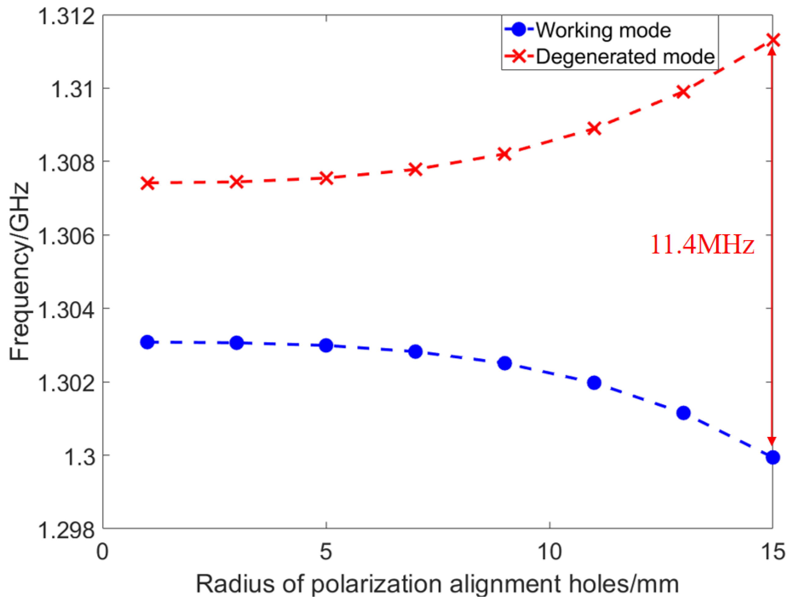
2.3. Mode Separation

TM 110 is the working mode in the deflecting cavity which exists degenerated modes. The present methods of mode separation are to break the rotational symmetry of the cavity and fix the polarization direction, which include adding holes on the disk [20], using racetrack shaped RF coupling iris [9], cutting slots on the edge of the cavity [12,16], adding longitudinal rods in the cavity [21], using an elliptical racetrack shaped cavity [22], etc. Due to the exist of coupling slot in the middle cell, the symmetry has been broken and the frequency separation value of the two degenerated modes is about 3 MHz. To further separate the frequency, adding polarization alignment holes is selected due to the 1.3 GHz deflecting cavity has large geometric size. As the polarization direction of the working mode is y-axis, the two polarization alignment holes are chosen to locate on x-axis with center-to-center distance of 128 mm. The holes locate where the degenerated mode has stronger electric field, and the working mode has stronger magnetic field to acquire the most outstanding mode separation effect. The frequency deviation of the two modes with different hole radius are shown in Figure 4, finally the radius of 15 mm is determined, and the frequency deviation of the two modes is greater than 10 MHz.
The final parameters of the deflecting cavity are shown in Table 2.

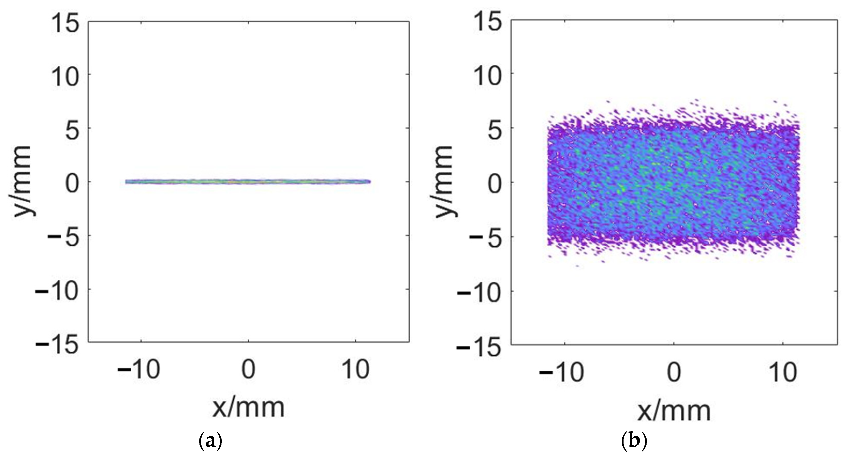
2.4. Particle Tracking Simulation

Figure 5 shows the design of the beamline to measure the electron beam bunch length of the miniaturized 150 kV DC photocathode gun. To evaluate the performance of the deflecting cavity, the simulation of bunch length measurement is carried out in General Particle Tracer (GPT) [23]. In this paper, the integrated deflecting voltage is calculated as
V d e f   = Δ p × v q   =   [ E y ( z ) e j k z β + j β c H x ( z ) e j k z β ] d z
where E y is the electric field intensity in vertical direction, H x is the magnetic field intensity in horizonal direction.
As the electron bunch energy is so low, the bunch is susceptible to the deflecting field and the longitudinal electric field when it is passing through the deflecting cavity. The former deflects the bunch as expected, but the later complicates the measurements. As the electron bunch has a finite transverse dimension of which the center is located along the cavity axis at the entrance, its upper and lower part sees the longitudinal electric field in opposite directions resulting in the increase of the energy spread and bunch lengthening. In addition, this effect will be aggravated with the space charge effect (SCE) making the transverse and longitudinal size larger and the electron bunch being kicked up as well as having a transverse offset. However, under the situation of low charge the SCE has little effect on result.
The electron beam distribution in 6D phase space generated by ASTRA [24] is used as the source for the GPT simulation. According to the ASTRA internal plateau distribution model, the bunch is generated from initial conditions set and the initial average kinetic energy of the total electron bunch is 0.9 eV with energy spread 0.63 eV. The initial RMS length of the plateau bunch is 6.05 ps with 0.42 mm transverse diameter after driving laser shaping. The normalized emittance calculated value of a cesium potassium antimonide photocathode is ~0.134 mm-mrad according to the thermal emittance measurement result of 0.56 mm-mrad/mm (@532 nm) at JLab [25]. Electron bunch with certain low charges are simulated and Table 3 shows the plateau bunch simulation results.
The simulated bunch length without SCE is 6.05 ps at the center of the cavity which is basically consistent to original value. According to Table 3, when the charge is lower than 100 fC, the SCE can be basically ignored. Therefore, to accurately measure the bunch length with low energy of 150 keV, the electron beam should be with a low charge density in the situation of low charge. Furthermore, the best resolution of the system is 590 fs with bunch charge of 50 fC and solenoid focus intensity of 214 Gauss.
From the simulation with different charge, when the electron bunch enters the cavity center at zero phase, all the transverse offsets of the average trajectory at the exit of cavity is about 2.79 mm. With the transverse offset, the average kinetic energy is increased from 150 keV to 151.5 keV due to the longitudinal electric field. The energy spread can be ignored after DC field and is increased differently with different charge due to Table 3 when leaving the deflecting cavity.
To further improve the temporal resolution as the initial charge is 50 fC and the solenoid is off, by introducing a 100-μm-gap horizontal slit placed 127 mm before the entrance of deflecting cavity the resolution can be improved to 190 fs. As the vertical size of the electron bunch becomes smaller after passing through the slit, the bunch hitting on the screen produces a narrower beam spot with cavity off and is kicked up with cavity on. Figure 6 indicates the bunch length measurement result at the screen with cavity off and on. In addition, the vertical RMS size are 0.18 mm and 5.84 mm, respectively. Simulation shows the resolution of the measurement system can reach to 190 fs with 50 kV deflecting voltage and the bunch length is 6.30 ps which is consistent with the actual value of 6.28 ps. Due to the exist of slit, the σ y , 0 becomes small and a better resolution has been achieved, but the charge of electron bunch becomes lower so CCDs with higher sensitivity are required.

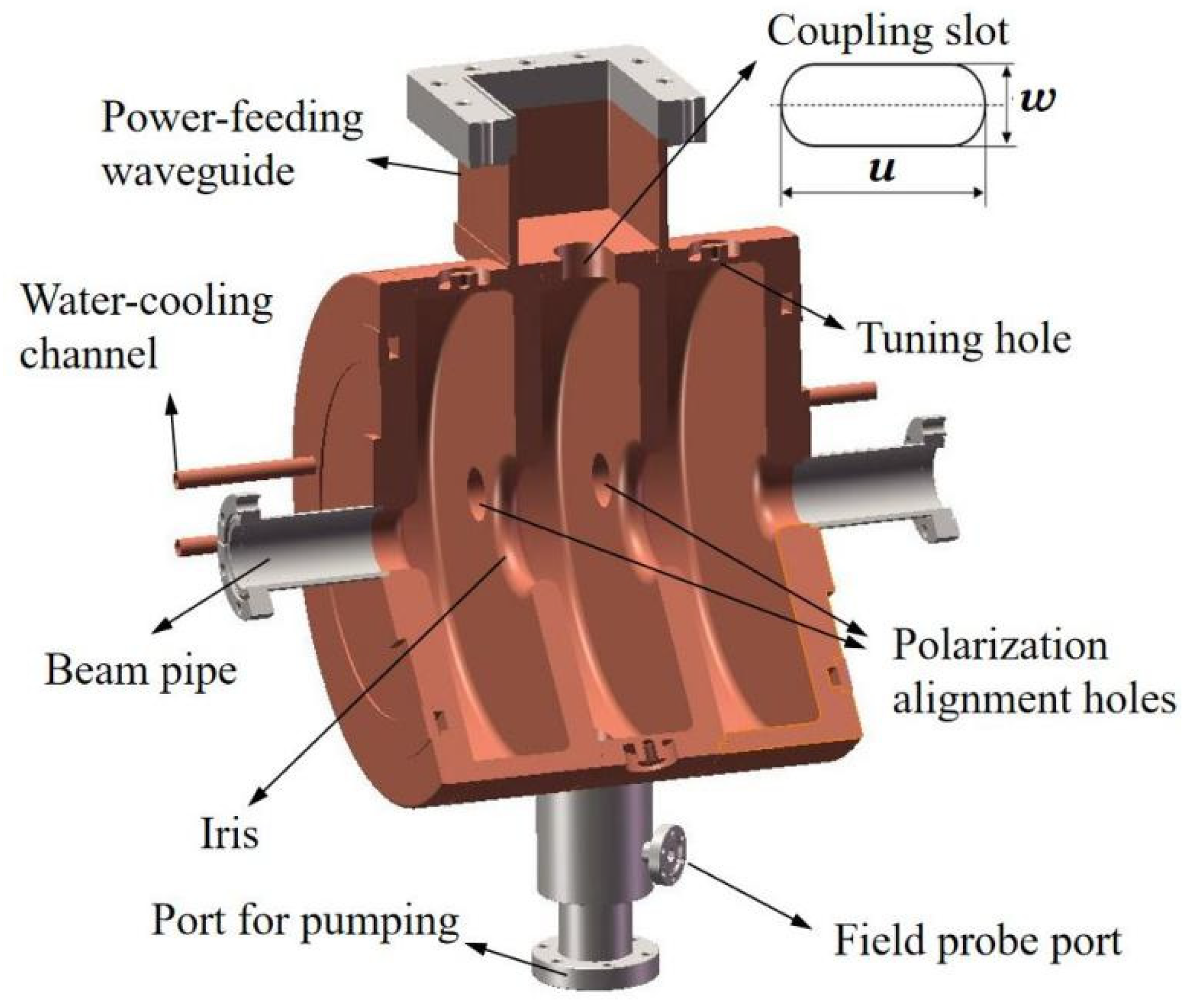
3. Mechanical Design

After completing the microwave design as well as particle tracking simulation, the 3D model of deflecting cavity is established and shown in Figure 7. In the mechanical design, there are three main goals. One is to ensure the limited frequency shift during pumping. The other one is to solve the brazing problem between the cavity and the coupler. The third one is to enable the cavity with the capability of frequency tuning.

3.1. Analysis of the Frequency Drift during Pumping

As the 1.3 GHz deflecting cavity operates in TM 110 mode, the coefficient of frequency shift with temperature is about −20.52 kHz/°C through calculation in CST, so the frequency shift of less than 20 kHz can be easily compensated either by adjusting water temperature or during the design. The deflecting cavity works in an ultra-high vacuum state, and the changed pressure would cause the surface deformation during pumping. For a uniform thickness cylindrical cavity, the deformation of the curved surface is smaller than the end walls, so the thickness of the curved surface and end walls are optimized separately for the deflecting cavity. Due to the weight and mechanical strength, the outer diameter of the cavity is chosen to be 296 mm, and the wall thickness of the end and middle cell are 11.76 mm and 15.61 mm, respectively. The frequency drift caused by the deformation of the curved surface is about 5 kHz, which can be ignored. The largest deformation and frequency drift with different end wall thickness during pumping are calculated. The results are listed in Table 4. When the end wall thickness is more than 21 mm, the frequency drift is within acceptable range. Simulation shows that maximum deformation is located around the root segment of the beam pipe, so setting stiffening rings around the beam pipe is proposed. Finally, the thickness of the end wall is 21 mm, the thickness and outer diameter of the stiffening ring are 5 mm and 118 mm, respectively. The cavity frequency deviation is −17.22 kHz due to the mechanical deformation from the atmosphere pressure to vacuum under the design.

3.2. Brazing Solution

For the 1.3 GHz deflecting cavity with geometric beta of 1, the length of a single cell is slightly longer than the width of the standard rectangular waveguide, so the waveguide can be brazed to the cavity directly. For the deflecting cavity with geometric beta of 0.634, its single cell length is shorter than the width of the standard rectangular waveguide, the rectangular waveguide occupies the top of the total middle cell and partial end cells, the conventional brazing method cannot be used here. In order to solve the brazing problem, a special transition plate is designed as shown in Figure 8. Its one side equipped arc surfaces and location steps which can be brazed with the middle cell equipping the corresponding arc surfaces and steps, and the other side is flat which can be brazed with the waveguide. By using the transition plate, the waveguide brazing has ignored influence on the end cells.

3.3. Tuning Holes Design

There may exist deviation between the actual frequency and the desired value when the fabrication of the deflecting cavity is completed. Therefore, the deflecting cavity is required to have frequency tuning capability. In this paper, perturbation of the cavity radius is adopted to tune the frequency.
The electric field of the working mode is concentrated inside the cavity, which is surrounded by the magnetic field. There is magnetic field distributing over the cavity wall concentrated on the upper and lower part, so volume perturbations of the magnetic field are performed to adjust the resonant frequency. The tuning scheme is carried out on all the three cells. One pair of tuning holes are located at the upper and lower part for each end cell and four tuning holes are placed at an angle of 45° from the y-axis for the middle cell. All the eight holes with reserved rods have the same size. The outer diameter of the tuning hole is 30 mm, and the remaining wall thickness is 4 mm. There are M8 screw threads in the center of each reserved rod with diameter of 16 mm, and the holes can be pushed or pulled to adjust the resonant frequency. The deformation produced by applying different forces to the tuners are calculated in CST. The results show that, when the adjustment is 627 kHz which has met the requirement, the deformation value is 0.54 mm.

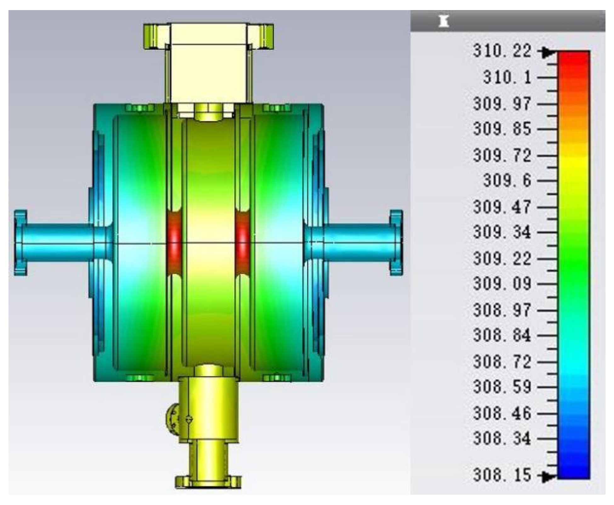
4. Thermodynamic Analysis

The microwave power of the normal-conducting deflecting cavity is mainly dissipated on the cavity wall. To prevent the rise in surface temperature from exceeding 1 °C and ensure stable operation, a water-cooling system is designed. When the repetition rate is of 10 Hz and pulse width is of 1 ms, the average power loss of the 3-cell deflecting cavity is 100 W with peak power of 10 kW, as the cavity works in the pulse mode instead of CW mode so the 1 ms pulse is long enough to the measurement.
The cooling design is slotting a C-type water channel at both end walls with a rectangular section of 12 mm × 6 mm. When the water flow is 3 L/min and the inlet water temperature is 35 °C, the temperature rise of the outlet water is about 0.48 °C, which leads to negligible changes in the physical parameters of cooling water, and the heat exchange coefficient is 4492 W/( m 2 ∙K). The temperature distribution of the deflecting cavity is calculated in CST. The result with 110 mm water ring radius is shown in Figure 9, in which the boundary condition is set as adiabatic.
The result shows that there is little difference between the wall temperature and water temperature, and the highest temperature is located at the iris of the disk. The frequency shift due to thermal expansion is 27.8 kHz from further calculation, which can be easily compensated.

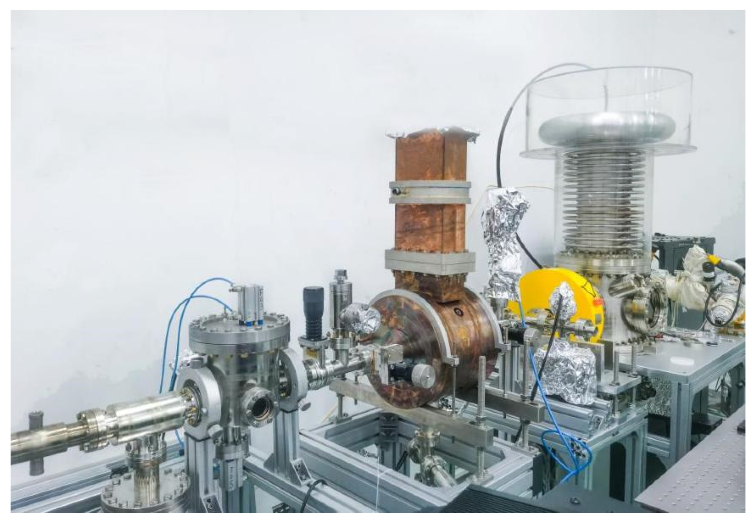
5. Fabrication and RF Measurement Results

After the completion of the whole design, a deflecting cavity made of oxygen-free high thermal conductivity copper is fabricated to reduce the ohmic losses. To guarantee the actual resonant frequency of the cavity is almost the same as the desired frequency, the radii of the three cells are slightly cut twice before brazing. Simulations indicate the frequency deviation
Δ f ( 2.6 × Δ b e 3.8 × Δ b m ) MHz / mm
where ∆ b m and ∆ b e are the radius variations of middle cell and one end cell, respectively. RF measurements are taken before the brazing using a vector network analyzer (VNA). The initial frequency is 1301.636 MHz at 21 °C. After all the three cells are cut 0.1 mm in radius, the change of the resonant frequency is 0.89 MHz, which is consistent well with the simulation results. The reference value of the second cutting value is 0.094 mm, and the measured resonant frequency is 1299.933 MHz at 21 °C. This frequency is within expectations, it is estimated to 1300.284 MHz after the cavity is pumping to vacuum due to the different inside dielectrics. Finally, the cavity can be operated at the frequency of 1300 MHz with cooling water with temperature of 35 °C which is the goal frequency. The deflecting cavity is brazed after the second cutting.
RF measurements of the deflecting cavity after brazing are carried out. The frequency of the cavity is 1299.932 MHz, Q 0 is 1.87 × 10 4 , Q e is 1.72 × 10 4 which are measured with the room temperature of 21 °C and under atmospheric pressure. The frequency of the deflecting cavity is almost unchanged before and after brazing as expected.
The field distribution of the working mode is measured by bead-pull method [26] shown in Figure 10. Meanwhile, one of the measurement results with normalized frequency change is also presented in Figure 10. The braided wire with a nominal diameter of 0.105 mm is used in the measurement which has much weaker ductility than commonly used nylon material wire, which can improve the measurement stability. The bead is a rotational symmetric cylinder with length of ~10 mm and diameter of ~1 mm made of aluminum tape, so that even in the process of pulling the wire, the rotation of the wire has little effect on the field distribution. As shown in Figure 10, a ~2 mm diameter hole is made in the center of the flange protector cover, and the wire is aligned through the small hole to ensure that the wire is on the axis, the deviation of the axis is controlled to be less than 1 mm. Eventually, the wire is pulled at a low speed which is less prone to jitter to acquire a stable and repeatable measurement result. Ten groups of measurements have been taken totally by using VNA, and the repeatability is quite good, the average value of the field flatness is 99.18 ± 0.08%. In conclusion, the measured values of the physical parameters are in good agreement with the simulation design ones.
The vacuum of deflecting cavity is reach to 2.3 × 10 7 Pa with ion pump after baking and is installed in beamline of the DC photocathode gun. The beamline is shown in Figure 11. Next, we will test the beamline and the bunch length measurement experiment will be taken in the near future.

6. Conclusions

A 1.3 GHz 3-cell medium- β ( β = 0.634) disk-loaded normal-conducting standing-wave deflecting cavity is systematic studied and fabricated to deflect electron beams with low energy of 150 keV. Benefiting from its simple structure, the cavity is quite easy for fabrication. The measured results of the cavity are in good agreement with the simulation. In addition, the cavity has been installed in the measurement beamline of 150 kV DC photocathode gun and the simulation results indicate the deflecting cavity can achieve a best resolution of 190 fs with the existing power amplifier.

Author Contributions

Conceptualization, Z.X., F.W., T.T. and Y.L.; methodology, Z.X. and F.W.; formal analysis, Z.X. and F.W.; investigation, Z.X. and F.W.; writing—original draft preparation, Z.X.; writing—review and editing, F.W.; supervision, S.H. and S.Q. All authors have read and agreed to the published version of the manuscript.

Funding

This research was funded by National Key R&D Program of China, grant number No. 2017YFA0701001.

Institutional Review Board Statement

Not applicable.

Informed Consent Statement

Not applicable.

Data Availability Statement

The data presented in this study are available on request from the corresponding author.

Acknowledgments

The authors want to show their gratitude to Lin Lin for providing the research material and methods.

Conflicts of Interest

The authors declare no conflict of interest.

References

  1. Bernd, S.; Sara, C.; Peter, S.; Stefan, S.; Manfred, T.; Axel, W.; Timo, K.; Thomas, S.; Volker, S.; Hans, S.; et al. Bunch Length Measurements at the SLS Linac Using Electro Optical Sampling. In Proceedings of the Free Electron Laser Conference, Trieste, Italy, 29 August–3 September 2004. [Google Scholar]
  2. Xuan, W.; Shouhua, N.; Hyuk, P.; Junjie, L.; Rick, C.; Renkai, L.; Xijie, W.; Jianming, C. Measurement of femtosecond electron pulse length and the temporal broadening due to space charge. Rev. Sci. Instrum. 2009, 80, 013902. [Google Scholar]
  3. Baum, P.; Zewail, A. Breaking resolution limits in ultrafast electron diffraction and microscopy. Proc. Natl. Acad. Sci. USA 2006, 103, 16105–16110. [Google Scholar] [CrossRef] [PubMed]
  4. Takao, I. High-resolution bunch-length monitor capable of measuring an rms value of a few mm. Nucl. Instrum. Methods A 1995, 361, 430–435. [Google Scholar]
  5. Wang, D.X.; Krafft, G.A.; Sinclair, C.K. Measurement of femtosecond electron bunches using a rf zero-phasing method. Phys. Rev. E 1998, 57, 2283–2286. [Google Scholar] [CrossRef]
  6. Gao, M.; Jean-Ruel, H.; Cooney, R.; Stampe, J.; de Jong, M.; Harb, M.; Sciaini, G.; Moriena, G.; Miller, R. Full characterization of RF compressed femtosecond electron pulses using ponderomotive scattering. Opt. Express 2012, 20, 12048–12058. [Google Scholar] [CrossRef] [PubMed]
  7. Shi, J.; Chen, H.; Tang, C.; Huang, W.; Du, Y.; Zheng, S.; Ren, L. RF deflecting cavity for bunch length measurement in Tsinghua Thomson scattering X-ray source. Chin. Phys. C 2009, 33, 161–164. [Google Scholar]
  8. Dolgashev, V.; Bowden, G.; Ding, Y.; Emma, P.; Krejcik, P.; Lewandowski, J.; Limborg, C.; Litos, M.; Wang, J.; Xiang, D. Design and application of multimegawatt X-band deflectors for femtosecond electron beam diagnostics. Phys. Rev. ST Accel. Beams 2014, 17, 102801. [Google Scholar] [CrossRef]
  9. Maesaka, M.; Inoue, S.; Ohshima, T.; Matsubara, S.; Higashiya, A.; Yabashi, M.; Shintake, T.; Otake, Y.; Ego, H.; Yanagida, K.; et al. Beam diagnostic system of XFEL/Spring-8. In Proceedings of the DIPAC’09, Basel, Switzerland, 25–27 May 2009. [Google Scholar]
  10. Craievich, P.; Bopp, M.; Braun, H.; Ganter, R.; Pedrozzi, M.; Prat, E.; Reiche, S.; Zennaro, R.; Grudiev, A.; Catalan, L.N.; et al. Sub-Femtosecond Time-Resolved Measurements Based on a Variable Polarization X-Band Transverse Deflecting Structures for SwissFEL. In Proceedings of the Free Electron Laser Conference, Santa Fe, NM, USA, 20–25 August 2017. [Google Scholar]
  11. Tan, J.; Gu, Q.; Fang, W.; Tong, D.; Zhao, Z. X-band deflecting cavity design for ultra-short bunch length measurement of SXFEL at SINAP. Nucl. Sci. Tech. 2014, 25, 060101. [Google Scholar]
  12. Sergey, B.; Ivan, B.; Valery, S.; John, S.; Karl, S.; Vadim, V. Deflecting cavity for beam diagnostics at Cornell ERL injector. Nucl. Instrum. Methods A 2014, 614, 179–183. [Google Scholar]
  13. McKenzie, J. Longitudinal Beam Characterisation on VELA Using a Transverse Deflecting Cavity. Ph.D. Thesis, University of Liverpool, Liverpool, UK, 2018. [Google Scholar]
  14. Nishimura, Y.; Sakaue, K.; Nishiyama, M.; Takahashi, T.; Washio, M.; Takatomi, T.; Urakawa, J. Design of a two-cell rf-deflector cavity for ultra-short electron bunch measurement. Nucl. Instrum. Methods A 2014, 764, 291–298. [Google Scholar] [CrossRef]
  15. Lin, X.; Zha, H.; Shi, J.; Zhou, L.; Liu, S.; Gao, J.; Chen, H. Development of a seven-cell S-band standing-wave RF-deflecting cavity for Tsinghua Thomson scattering X-ray source. Nucl. Sci. Tech. 2021, 32, 36. [Google Scholar] [CrossRef]
  16. Sunjeong, P.; Hyun, W.; Mi, H.; Young, C.; In, H.; Kyu-Ha, J.; Eun-San, K.; Hongjoo, K.; Nikolay, A.; Young, U.; et al. Measurement of low-energy and low-charge ultrashort bunches using an S-band RF deflector. Nucl. Instrum. Methods A 2019, 927, 194–201. [Google Scholar]
  17. van Oudheusden, T.; Pasmans, P.L.E.M.; der Geer, S.B.; de Loos, M.J.; van der Wiel, M.J.; Luiten, O.J. Compression of Subrelativistic Space-Charge-Dominated Electron Bunches for Single-Shot Femtosecond Electron Diffraction. Phys. Rev. Lett. 2010, 105, 264801. [Google Scholar] [CrossRef] [PubMed]
  18. Matsuba, S.; Honda, Y.; Miyajima, T. Deflecting cavity for bunch length diagnostics at compact ERL injector. In Proceedings of the 1st International Particle Accelerator Conference, IPAC, Kyoto, Japan, 23–28 May 2010. [Google Scholar]
  19. CST (Computer Simulation Technology) Studio Suite. Available online: http://www.cst.com (accessed on 12 March 2021).
  20. Akre, R.; Bentson, L.; Emma, P.; Krejcik, P. A transverse RF deflecting structure for bunch length and phase space diagnostics. In Proceedings of the Particle Accelerator Conference, Chicago, IL, USA, 18–22 June 2001. [Google Scholar]
  21. David, A.; Giampiero, D.; Luca, F.; Andrea, M.; Luigi, P.; James, R.; Cristina, V. RF deflector design and measurements for the longitudinal and transverse phase space characterization at SPARC. Nucl. Instrum. Methods A 2006, 568, 488–502. [Google Scholar]
  22. Ambattu, P.K.; Burt, G.; Grudiev, A.; Dolgashev, V.; Dexter, A. Coupler induced monopole component and its minimization in deflecting cavities. Phys. Rev. ST Accel. Beams 2013, 16, 062001. [Google Scholar] [CrossRef]
  23. General Particl Tracer (GPT). Pulsar Physics. Available online: http://www.pulsar.nl/gpt/ (accessed on 16 June 2021).
  24. A Space Charge Tracking Algorithm (ASTRA). Available online: http://www.desy.de/~mpyflo/ (accessed on 18 July 2021).
  25. Wang, Y.; Mamun, M.A.; Adderley, P.; Bullard, B.; Grames, J.; Hansknecht, J.; Hernandez-Garcia, C.; Kazimi, R.; Krafft, G.A.; Palacios-Serrano, G.; et al. Thermal emittance and lifetime of alkali-antimonide photocathodes grown on GaAs and molybdenum substrates evaluated in a −300 kV dc photogun. Phys. Rev. Accel. Beams 2020, 23, 103401. [Google Scholar] [CrossRef]
  26. Shi, J.; Alexej, G.; Walter, W. Tuning of X-band traveling-wave accelerating structures. Nucl. Instrum. Methods A 2013, 704, 14–18. [Google Scholar] [CrossRef]
Figure 1. The two-dimensional drawing of the 3-cell deflecting cavity.
Applsci 12 09243 g001
Figure 2. The relationship between R and the electron beam β .
Applsci 12 09243 g002
Figure 3. The electromagnetic field of the working mode.
Applsci 12 09243 g003
Figure 4. The influence of the polarization alignment holes radius on the mode frequency separation.
Applsci 12 09243 g004
Figure 5. The design of the bunch length measurement beamline.
Applsci 12 09243 g005
Figure 6. Electron beam profile at the screen in the GPT simulation. (a) Deflecting cavity is off; (b) Deflecting cavity is on.
Applsci 12 09243 g006
Figure 7. Three-dimensional mechanical model of the deflecting cavity.
Applsci 12 09243 g007
Figure 8. Schematic of the waveguide brazing with the middle cell. (a) Transition plate; (b) Main part of cavity; (c) After brazing.
Applsci 12 09243 g008
Figure 9. Temperature distribution of the cavity with water cooling.
Applsci 12 09243 g009
Figure 10. Bead-pull measurement device with measurement result. (a) The measurement device; (b) One of the measurement results.
Applsci 12 09243 g010
Figure 11. Measurement beamline installing.
Applsci 12 09243 g011
Table 1. The geometric dimension of the 3-cell deflecting cavity.
ParametersbmbedtRa
Value132.29136.1457.24163317.5
Table 2. Design parameters of the deflecting cavity.
ParametersDesign Value
Beam energy E [keV]150
Operation frequency f [MHz]1300
Transverse shunt impedance R [MΩ]0.98
Quality factor Q 0 19,500
RF input power P [kW]2.6
Deflecting voltage V d e f [kV]50
Expected temporal resolution Δ t [fs]<200
The frequency of π-mode in y-direction [MHz]1299.93
The frequency of π/2-mode in y-direction [MHz]1312.69
The frequency of 0-mode in y-direction [MHz]1335.19
The frequency of π-mode in x-direction [MHz]1311.33
The frequency of π/2-mode in x-direction [MHz]1317.71
The frequency of 0-mode in x-direction [MHz]1352.87
Table 3. The results of bunch length simulation with SCE under 50 kV deflecting voltage.
Bunch
Charge/fC
Solenoid Focus
Intensity/Gauss
Bunch-Length
Actual Value/ps
Simulated Value (Resolution)/psEnergy Increase/keVEnergy Spread
502146.286.31 (0.59)1.51.32%
1002156.506.55 (0.60)1.51.37%
2002186.936.99 (0.65)1.51.42%
5002248.108.17 (0.88)1.51.86%
Table 4. Simulation results of the largest deformation and frequency drift with different end wall thickness.
End Wall Thickness/mmLargest Deformation/mmFrequency Drift/kHz
100.0609−69.19
150.0266−33.57
210.0142−19.55
230.0119−16.75
250.0101−14.48
Publisher’s Note: MDPI stays neutral with regard to jurisdictional claims in published maps and institutional affiliations.

