1. Introduction
In the past few decades, detectors based on microchannel plates (MCP) and position sensitive anodes have been widely used in neutron detection [
1], biomedical imaging [
2,
3], X-ray spectroscopic measurement [
4], and aerospace [
5,
6]. Direct readout is the traditional readout to directly collect the electron cloud emitted from MCP by metal anodes. It arouses the redistribution of secondary electrons on the anode, which results in image instability. Luckily, charge induction readout technology overcomes these problems and also provides significant performance and practical advantages. Different from the direct readout, the charge induction readout has a resistive layer between the MCP and the anode. The electrons fall on the resistive layer, and then the signal is coupled to the anode. Compared with direct readout, charge induction readout can eliminate the secondary electron-mediated charge redistribution noise and avoid the influence of an uneven electrostatic field on the electron movement, so it is beneficial to improve the image linearity. In addition, the resistive layer can play the role of electrical and physical isolation, which facilitates the packaging and modularization of the detector. The anode is located outside the vacuum chamber and is easy to replace.
There is much research concerning on the MCP imaging detector with a charge induction readout. In 2002, Jagutzki introduced the charge induction readout into a wedge and strip anode (WSA) detector, obtaining similar image resolution to that of direct readout [
7]. In 2003, Lapington developed an open-faced position-sensitive detector by combining a WSA and charge induction readout for the SPIDER mission. It overcomes the major WSA deficiency of image instability resulting from secondary electron-mediated charge redistribution on the anode [
8]. In 2013, Jagutzki applied the charge induction readout technology to an intensifier and combined it with a delay line (DL) anode to form a detector for space- and time-correlated single photon counting [
9]. In 2015, Ni applied charge induction readout to a curved MCP detector, reducing the influence of MCP curvature on charge cloud size. The resulting imaging detector fulfilled the requirements of the Moon-based EUV camera [
10]. In 2020, Han developed photon-counting imaging for Aurora Observations based on WSA and charge induction [
11]. Charge induction readout technology is popular and has been used on various occasions, but there is still a lack of exploration in the case of cross-strip (XS) anode.
As the most recent developments of anodes, the XS anode has the advantages of high spatial resolution, good linearity, and low gain requirement [
12,
13]. Different from the planar structure of the WSA and DL anodes, the XS anode has two mutually perpendicular anodes. The three-dimensional anode pattern will affect the anode charge distribution in the process of electric field coupling. Therefore, it is necessary to carry out theoretical and simulation research to design detector parameters. Here, a new photon imaging detector combining charge induction readout with an XS anode is developed. This XS detector is expected to achieve the detection of particles (such as photons, ions, neutrons, and electrons) with a good imaging performance. In
Section 2, the operation of an XS anode detector with a resistive layer is introduced. Through theoretical research, the sheet resistance and substrate thickness of the resistive layer are given. A three-dimensional finite element model is established, and the anode parameters, including strip electrode width and insulation thickness, are designed from the perspective of optimizing the induced charge distribution on the XS anode and the inter-electrode capacitance between strips. In
Section 3, the XS anode is manufactured and the parameters are given. To characterize the detector, a test system is set up. In
Section 4, the designed anode is measured, and the small difference between measurement and simulation proves the accuracy of the model. The performance of the XS detector is tested with the resolution plate and full field illumination. The results indicate that the XS detector can achieve a resolution of 44.2 μm with a periodic distortion about 25.8%. Meanwhile, the calculation results of the same raw data with different algorithms show that a modified center of gravity (MCoG) is the optimal centroiding algorithm.
2. Design of Detector Parameters
2.1. Detector Operation
The developed XS detector consists of a Kovar-alumina brazed body assembly containing MCP stacks, resistive layer, and XS anode. The schematic diagram of XS detector operation is depicted in
Figure 1. First, the incident particle is converted into an electron cloud of 10
6–10
7 electrons by the MCP stack. Then, these electrons are accelerated by the electric field to the resistive layer, and induced charge pulses are generated on the XS anode strips because of the change of the electromagnetic field. Finally, the position of incident photons can be inversed by calculating the charge collected by the anode. The MCP stack is formed by using two MCPs with one placed on top of another with a bias angle of 13°. The resistive layer is a ceramic substrate coated with high-resistance germanium film; a −200 V is applied across the MCP-to-resistive layer gap by using a resistor mounted on the external wall of the brazed body.
2.2. Resistive Layer
The resistive layer and the readout anode can be viewed as a distributed two-dimensional RC network in the finite element approximation, as depicted in
Figure 2, where
Rs is the sheet resistance of resistive layer and
Ctotal is the total equivalent capacitance between the resistive layer and the anode.
ρ (
x,
y) indicates the point where the electron cloud lands on the resistive layer.
C1 to
CN represent the capacitances between the germanium film and each anode strip, respectively. The total capacitance
Ctotal is dependent on capacitances
C1 to
CN and the inter-electrode capacitances
Cij (
i = 1 to
N,
j = 1 to
N,
I ≠
j) between anode strips. Additionally, the readout circuits are presented by a charge-sensitive amplifier (CSA) in the red dotted box.
The induced charge on the anode is affected by the sheet resistance of the resistive layer. If the sheet resistance is too low, the transmission to the electrode decreases, whereas a too-high sheet resistance results in the decrease in resolution and count rate because of the electron cloud overlapping. When the electron cloud diffuses on the resistive layer, the charge density distribution can be expressed as [
14]:
where, in this case,
τ =
RsCtotal. N is the number of incident electrons. Clearly, the variation of the density distribution function of the charge cloud is related to the broadening width
σ and time constant
τ. The charge cloud broadening σ can be adjusted by changing the gap distance and gap voltage, which is generally about 0.5 mm. Given that
Trc is the duration of the electron cloud on the resistive layer, which satisfies
. To avoid overlapping,
Trc needs to satisfy
t < 1/(5 ×
Ncnts);
Ncnts is the counting rate of detector. As much energy as possible needs to be transmitted to the anode to achieve high energy utilization. A sheet resistance of 50 MΩ is finally chosen to satisfy the above requirements.
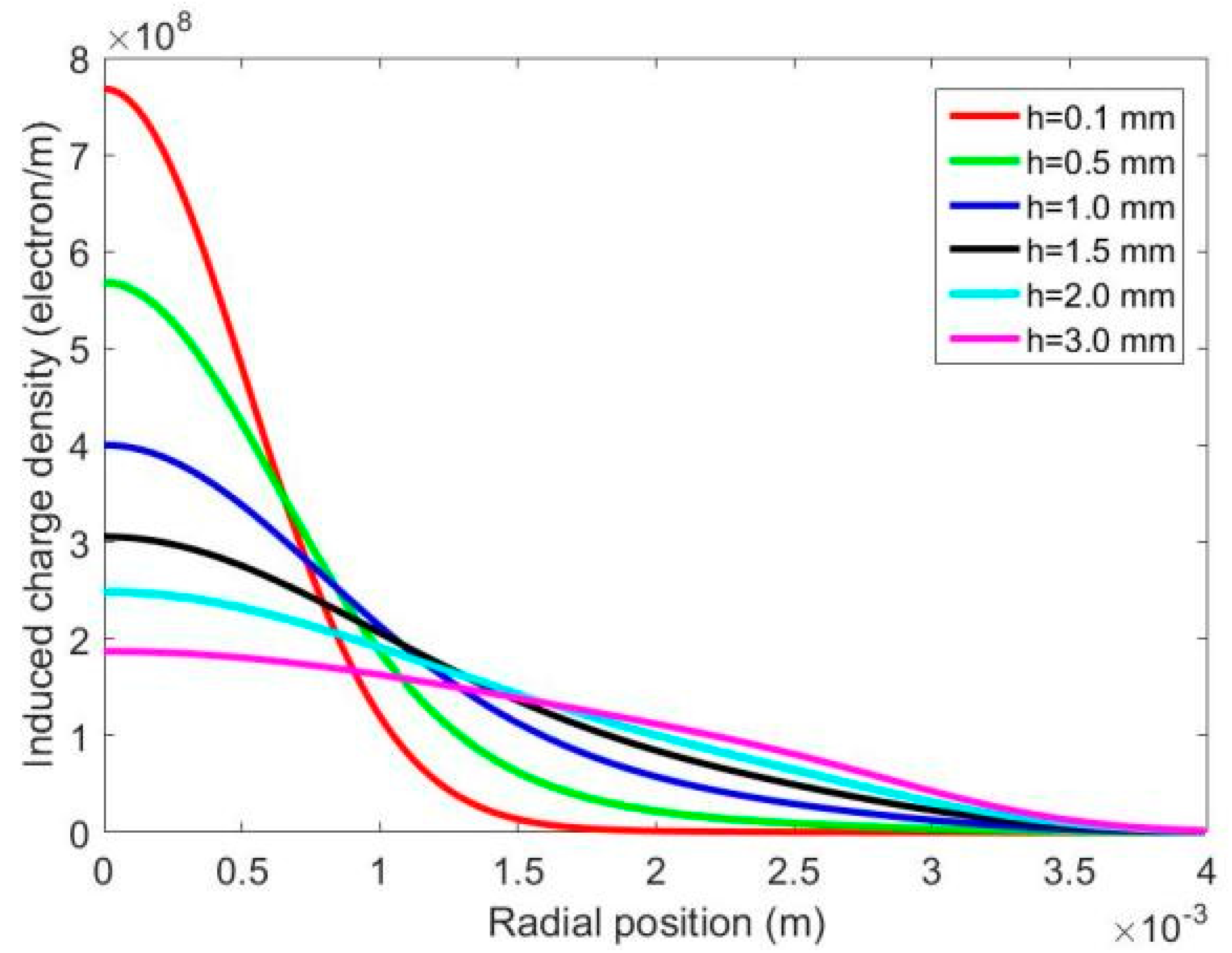
The width of the induced charge cloud footprint at the plane of the anode obviously must be optimized to match the XS anode. Indeed, a too-narrow footprint results in an under-sampled charge distribution. At the same time, a too-wide charge footprint leads to charge division between a large number of anode electrodes and, consequently, to the reduction in the signal-to-noise ratio (especially at the edge of the charge distribution). The charge density on the resistive layer as a function of radius for different substrate thickness is shown in
Figure 3. It is seen that the thicker the substrate thickness, the more dispersed the induced charge footprint, which prevents accurate centroid decoding. The substrate thickness of 0.5 mm is found to be optimal as five to seven strips must be covered.
2.3. XS Anode
The XS anode is a metal and ceramic cross-strip pattern structure with 32 + 32 strips for the top and bottom layers, respectively. For planar anodes, the amount of charge received on each anode is mainly related to its exposed area and charge distribution. For an XS anode with a double-layer structure, the top-layer anode will shield the bottom anode to some extent. The difference of charge amount between top and bottom layers will affect the signal-to-noise ratio in different spatial directions and the selection of amplifiers.
A detector composed of an XS anode and a resistive layer in the electric field satisfies Maxwell’s equations. It is assumed that there is a weak current density caused by the electric field. Therefore, the magnetic flux density B is negligibly small. Then the charge of the anode can be achieved by the Gauss’s law [
15]:
where
ε is the dielectric constant,
V is potential,
is free charge density. To reveal the relationship between the induced charge collected by the anode and its structure, the resistive layer and XS anode model are established by COMSOL, as shown in
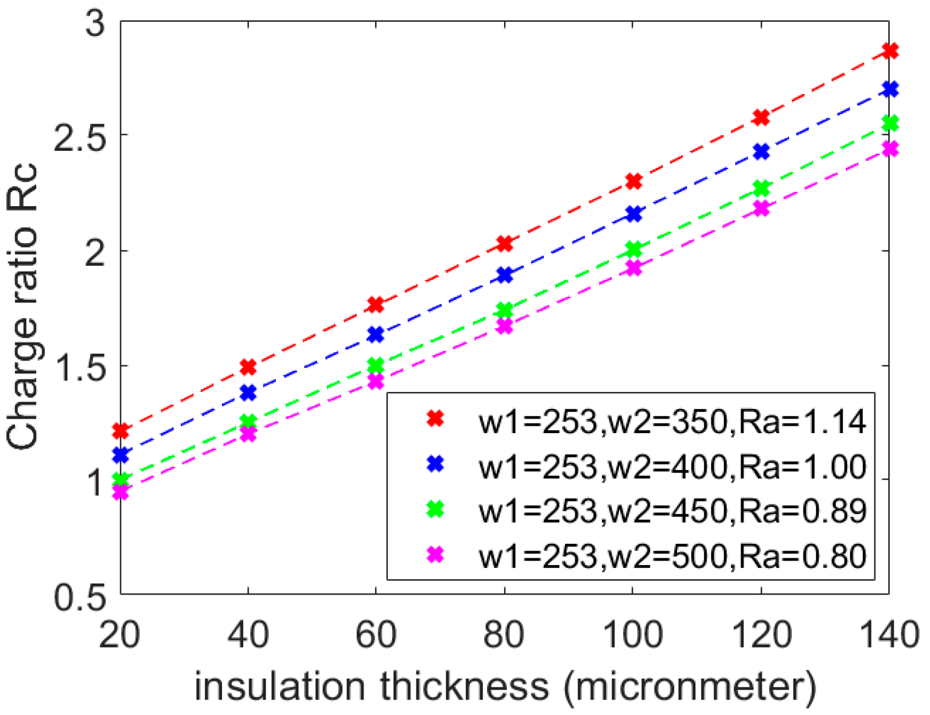
Figure 4. An electron cloud is generated on the resistive layer according to Equation (1), and the amount of induced charge on anode strips is integrated. The charge ratio of top and bottom anodes
Rc as a function of insulation thickness for different exposed area ratio
Ra is shown in
Figure 5.
It can be seen that for the same exposed area, the charge ratio increases linearly with the increase in insulation thickness. For the anode of Ra = 1, the charge ratio Rc is greater than 1. This is because the bottom strip is farther away from the resistive layer and the electric shielding effect of the top strip. For the same insulation thickness, the charge ratio Rc decreases with the increase of the exposed area ratio Ra. The initial broadening and central falling point of the electron cloud on the resistive layer also affect the charge ratio, so Rc is an average value. Based on the above rules, the anode parameters could be designed and the charge amplifier with appropriate magnification could be selected.
2.4. Crosstalk Effect of the Inter-Electrode Capacitance
The spatial resolution of the XS anode is primarily determined by the electronic noise, which is mainly induced by the charge-sensitive amplifier (CSA) and increases with input capacitance adding [
16]. The anode is a periodic structure, and the circuits of each channel are independent of each other. The capacitance of one channel is:
where
Ci is the strip electrode capacitance,
Cie is the inter-electrode capacitance of the anode strip,
Ca is the amplifier input capacitance,
Cf is the feedback capacitance, and
A is the open loop gain of the integrated amplifier. Crosstalk directly affects the signals on the strip electrodes because of the inter-electrode capacitance
Cie of the XS anode. Optimization of the inter-electrode capacitance is conductive to reduce the electronic noise.
For an ideal XS anode, the charges on the strips could be expressed as:
However, the crosstalk effect cannot be neglected in practice. The expression of charges on strips can be written in Maxwell’s capacitance matrix:
where
Cii is the capacitance of strip
i to the vacuum chamber,
Cij is the capacitance between the strip
i and
j,
Cij =
Cji. Substituting Equation (5) into Equation (4), the relationship between the ideal charge and the actual charge can be obtained, and the charge can be corrected to remove crosstalk.
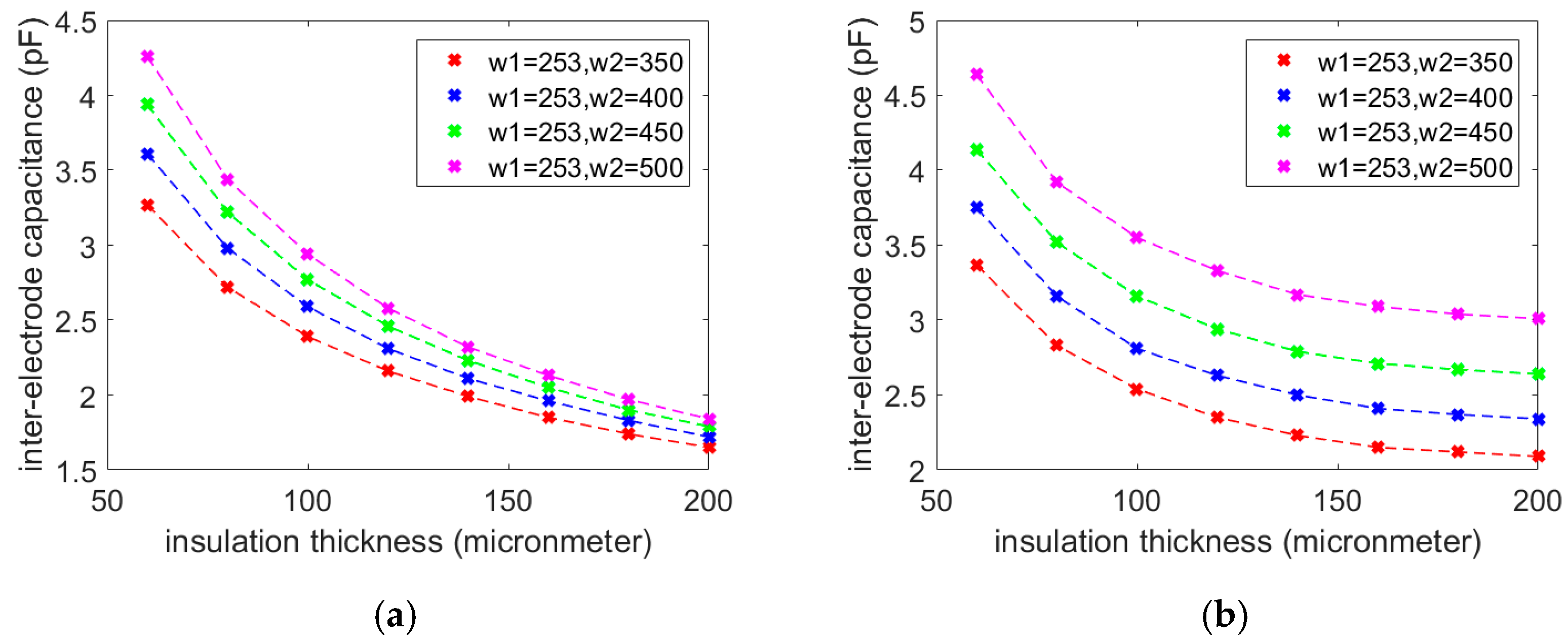
The XS anode model established by COMSOL mentioned earlier is also used to optimize inter-electrode capacitance. Taking one top strip and one bottom strip as examples, the variation of total inter-electrode capacitance (
) with insulation thickness for different strip widths is depicted in
Figure 6. It can be seen that, for the same strip width,
Cie decreases with the increase in insulation thickness. For the same insulation thickness,
Cie increases with the increase in strip width. The top and bottom strips can be regarded as parallel plate capacitors. The width of the strip and insulation thickness corresponds to the area of the capacitor plate and the dielectric thickness, respectively. This explains the variation of inter-electrode capacitance with different parameters.
To sum up, reducing the inter electrode capacitance requires increasing the thickness of the insulation layer and reducing the width and area of the strip. However, this will lead to the imbalance of charge ratio and the reduction in power utilization. Therefore, when designing anode parameters, it is necessary to comprehensively consider the system requirements and make trade-offs.
3. Experiment
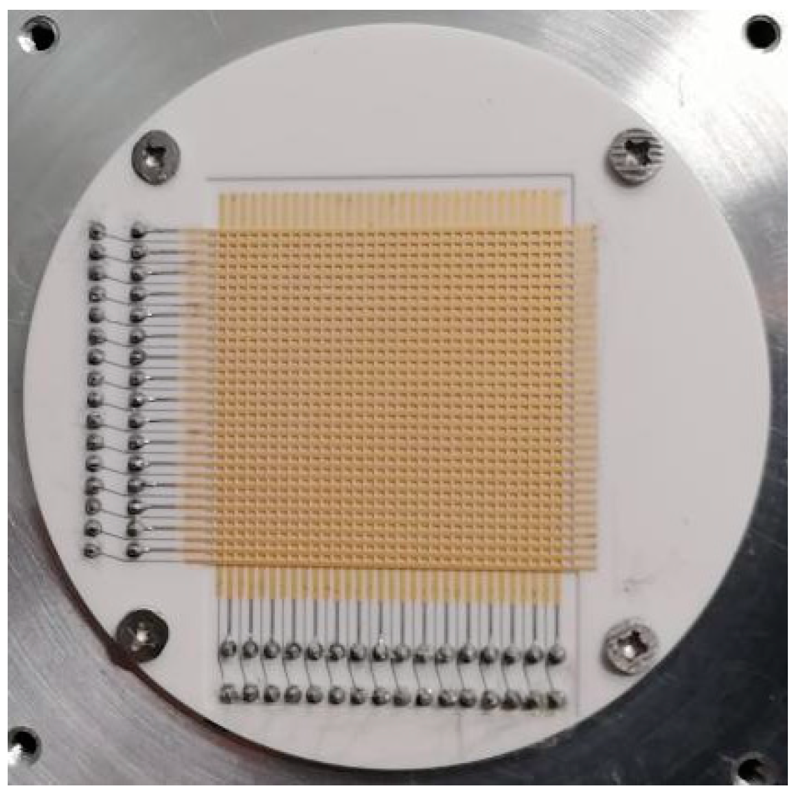
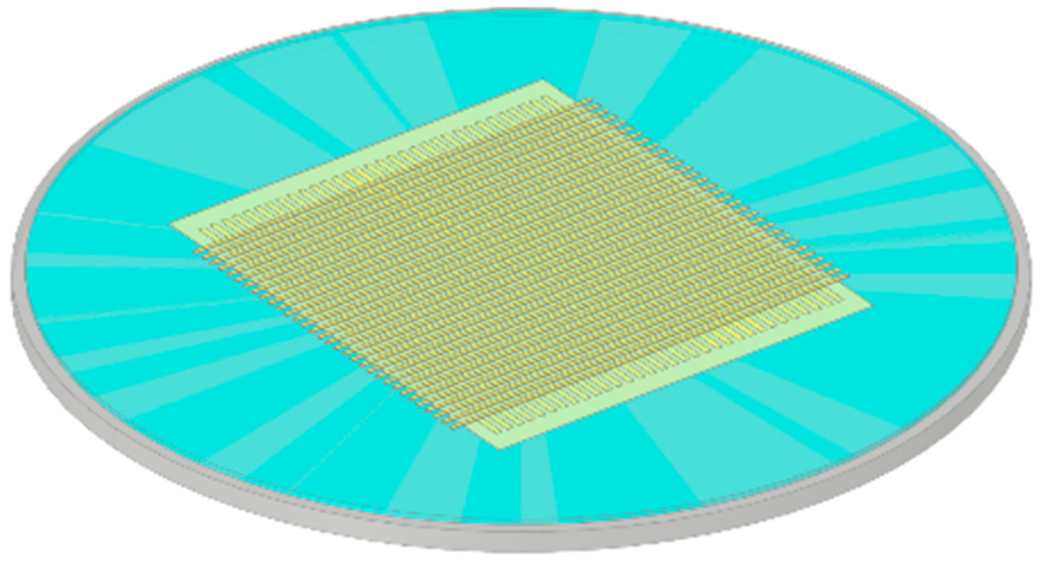
The 32 + 32 XS anode is manufactured by low-temperature cofired ceramic (LTCC) technology, as shown in
Figure 7. The whole process includes casting, drilling, through-hole filling, electrode printing, lamination, hot pressing, slicing, cofiring, etc. The design parameters are listed in
Table 1.
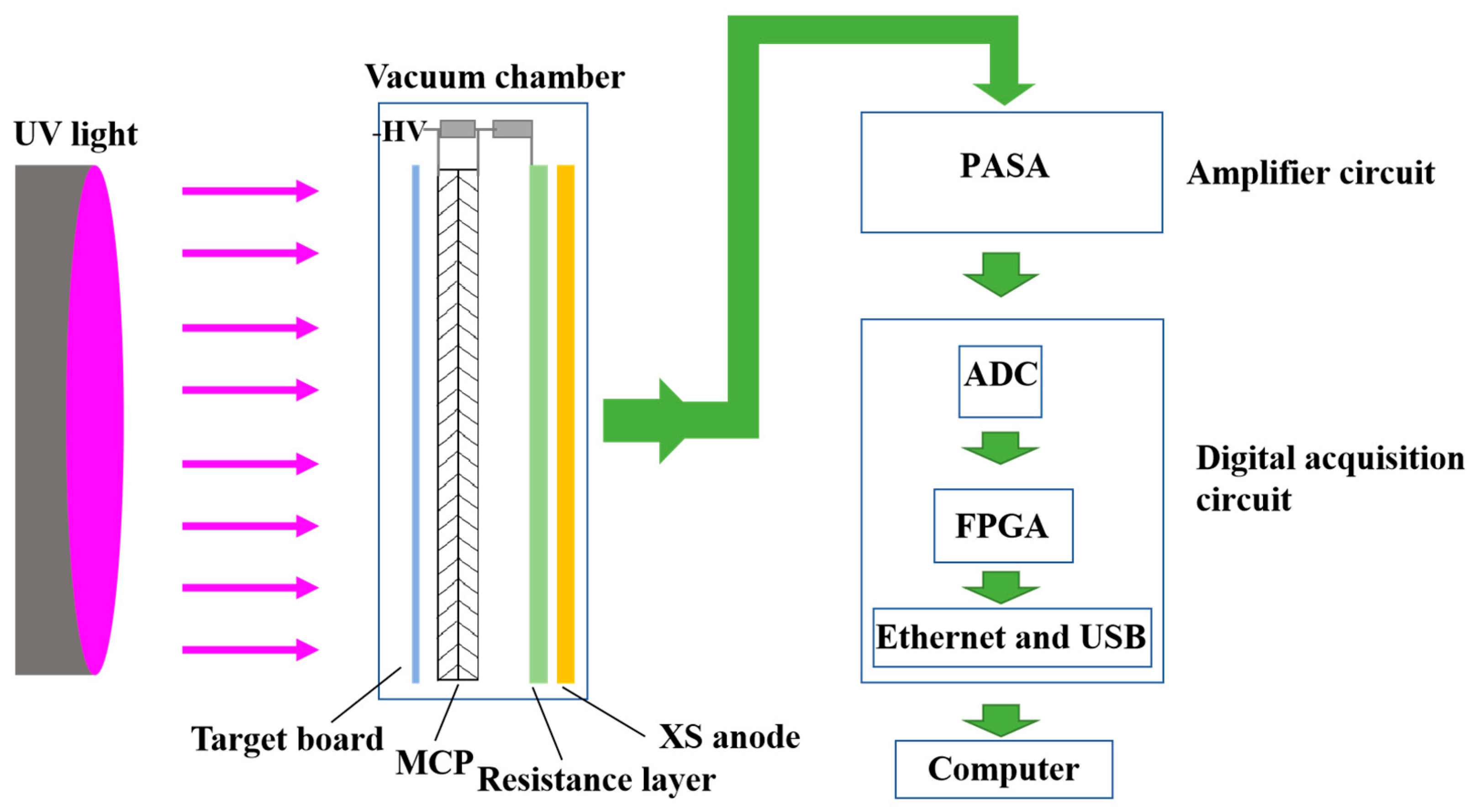
To evaluate its performance in spatial resolution and image linearity, the detector is placed in a vacuum chamber with a pressure of about 10
−5 pa. As shown in
Figure 8, an ultraviolet beam is used to illuminate the target board located in front of the detector. A negative high voltage is applied to the MCP stacks and the MCP-to-resistive layer gap via two resistors connected in series.
The signal processing electronics of the detector consists of 64 pre-amplifier shaping amplifiers (PASA), analog-to-digital converters (AD9257, ADI), and control (Spartan6, Xilinx) and interface circuits (RTL8211EG, REALTEK; CY7C68016A, CYPRESS). Each 64-channel signal is amplified and shaped, and then converted into digital form and sent to the FPGA. When the amplitude of the signal reaches the preset threshold, the sampling logic of FPGA is triggered and the data are transmitted to the computer through optical fiber or USB. The decoding software subsequently converts data to X, Y coordinates.
4. Results and Discussion
4.1. Results of Simulation and Measurement
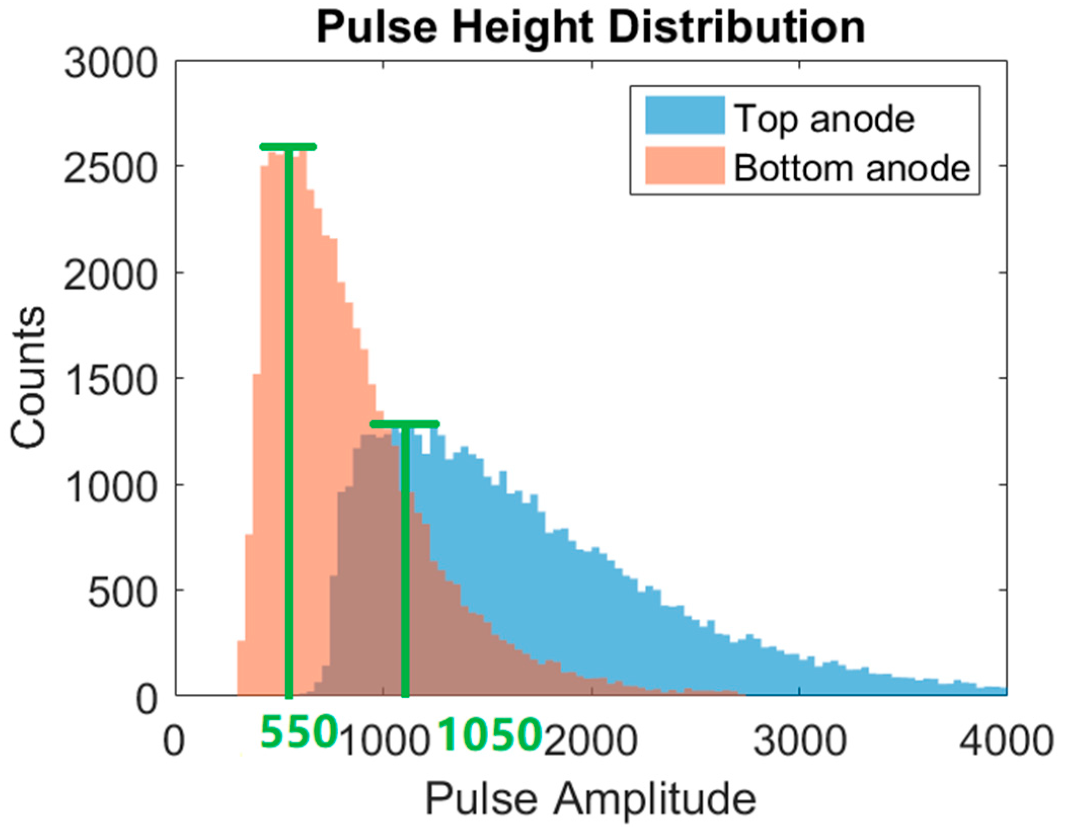
The same amplifier groups are used to collect the anode signal, and pulse height distribution of the top and bottom anode are measured, as shown in
Figure 9. The charge ratio of top and bottom anode is about 1.9, which is consistent with the simulation results.
Table 2 shows the simulated and measured capacitance for the XS anode. The relative norm difference of the results is used and defined as:
where
CS is the simulated capacitance and
CM is the measured capacitance. It can be seen that the simulated capacitance is about 9% larger than those of measured values. Due to machining error and geometry defect of the anode being neglected, the errors of inter-electrode capacitance are introduced. However, the minor difference between the simulation and measurement proves the reliability of the model.
4.2. Spatial Resolution
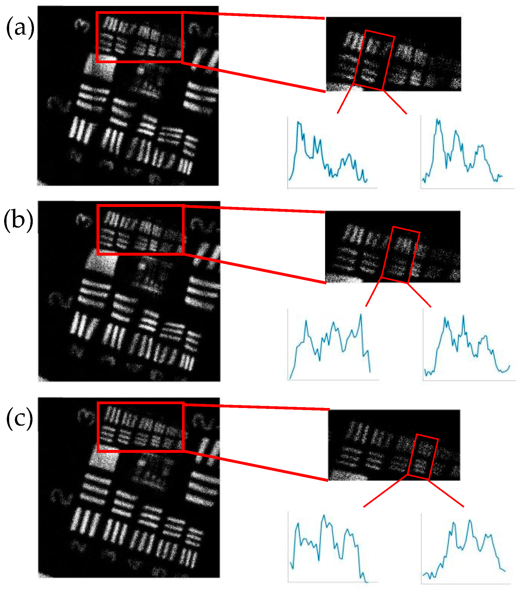
To characterize the resolution of the XS detector, a USAF1951 spatial resolution target in contact with the detector was illuminated by using a UV light. The basic concept of the centroiding algorithm is to calculate the central position of the incident photon using the charge value collected by each strip according to the induced charge distribution projection on two axes. Well-known decoding algorithms are Gaussian 3 strip (G3S), Gaussian 5 strip (G5S), and modified center of gravity (MCoG), which are summarized in
Table 3. G3S and G5S, respectively, use three and five strips to fit the induced charge cloud as a Gaussian function. Modified center of gravity (MCoG) is the simplest and fastest method among all centroid algorithms, while its threshold depends on the noise of the system and distribution of induced charge [
17]. For comparison, three centroiding algorithms have been used for decoding the same raw data, and the result images are shown in
Figure 10.
It is clear that the image of Group 3 Element 2 of the resolution target pattern obtained with G3S can be resolved, which means the spatial resolution in this case is 55.7 μm. The image of G5S has a better result and reaches a resolution of 49.6 μm (Group 3 Element 3). This is because G5S takes more strips into account to deduce distortions caused by various noise (readout noise, inaccuracies in anode geometry and amplifiers gain nonlinearity, etc.). MCoG resolves 44.2 μm (Group 3 Element 4) and the distortion is substantially less than that of G3S and G5S. The reason why MCoG has a better imaging result than Gaussian fitting is that the mismatch between charge distribution on anode and Gaussian function. In the charge induction readout mode, due to the discontinuous structure and geometric deviation of the anode, Gaussian function cannot accurately describe the charge distribution on the XS anode. MCoG takes the charge of the strip as the weight factor of the distance and has a floating threshold, which is more suitable for describing the charge distribution on the anode.
4.3. Periodic Distortion
Global uniformity is studied with full field illumination. The images shown in
Figure 11 are obtained with G3S, G5S, and MCoG centroiding respectively. There is an obvious periodic fixed pattern in the image, which is related to the XS anode periodic structure.
To characterize the fixed pattern of different centroiding algorithms, the photon distribution of a four-anode periods region in the image is counted. It is clear that G3S centroiding has severe periodic distortion. G5S and MCoG centroiding have less periodic distortion. The contrast of the fixed pattern can be obtained by:
where
Nmax and
Nmin are the number of photons in the peak and valley region of an anode period, respectively. Three centroiding algorithms are compared in terms of resolution, periodic distortion, complexity, and computation speed, and the results are shown in
Table 4. It is clear that MCoG has the best performance.
5. Conclusions
In this paper, an XS imaging detector with high resolution and low gain requirement is designed and developed by combining the charge induction readout mode with an XS anode. Through theoretical analysis, it is determined that the resistance of the resistance layer is 50 MΩ and the ceramic substrate thickness is 0.5 mm. The charge distribution and inter-electrode capacitance calculation model of an anode are established to study the effects of anode strip width and insulation thickness on anode charge distribution and inter-electrode capacitance. Based on this relationship, the parameters of the anode are designed. The widths of the top and bottom strips are 253 μm and 475 μm, respectively, the period width is 690 μm, and the insulation thickness is 100 μm. The small difference between the simulation and the measurement proves the reliability of the model. With signal processing electronics and decoding software, a complete XS detector test system is established. The XS detector is characterized to have a spatial resolution of 44.2 μm and a periodic distortion of 25.8%, decoding with MCoG, which is proved to have the best overall performance. In summary, the combination of charge induction readout and XS anode gives superior performance and higher integration, and the developed XS imaging detector has broad applications in electron, thermal neutron, X-ray, ultraviolet, and visible light detection and imaging.
Author Contributions
Conceptualization, Q.N. and Z.J.; methodology, Q.N. and Z.J.; software, Z.J.; validation, Q.N. and Z.J.; formal analysis, Q.N. and Z.J.; investigation, Q.N. and Z.J.; resources, Q.N.; data curation, Q.N. and Z.J.; writing—original draft preparation, Z.J.; writing—review and editing, Z.J.; visualization, Z.J.; supervision, Q.N. and Z.J.; project administration, Q.N.; funding acquisition, Q.N. All authors have read and agreed to the published version of the manuscript.
Funding
This work was supported by the National Natural Science Foundation of China under Grants No. 62135015 and No. 61675201.
Data Availability Statement
Not applicable.
Conflicts of Interest
The authors declare no conflict of interest.
References
- Montcel, B.; Torregrossa, M.; Poulet, P. Optode Positioning in Time-Resolved Neurological Nearinfrared Imaging. In Proceedings of the Biomedical Topical Meeting, OSA Technical Digest, Miami Beach, FL, USA, 14–17 April 2004; p. WF11. [Google Scholar]
- Rueck, A.; Dolp, F.; Scalfi-Happ, C. Time-Resolved Microspectrofluorometry and Fluorescence Lifetime Imaging Using Ps Pulsed Diode Lasers in Laser Scanning Microscopes. In Proceedings of the European Conference on Biomedical Optics, Munich, Germany, 22 June 2003; pp. 5139–5166. [Google Scholar]
- Fang, B.; Luan, K.; Ye, J. Linearly excited indium fluorescence imaging for temporally resolved high-precision flame thermometry. Opt. Lett. 2020, 45, 3957–3960. [Google Scholar] [CrossRef] [PubMed]
- Tremsin, A.S.; Siegmund, O.; Hull, J.S. High Resolution Photon Counting Detection System for Advanced Inelastic X-ray Scattering Studies. In Proceedings of the 2006 IEEE Nuclear Science Symposium Conference Record, San Diego, CA, USA, 16 May 2007; pp. 735–773. [Google Scholar]
- Zhang, X.; Chen, B. Wide-field auroral imager onboard the Fengyun satellite. Light. Sci. Appl. 2019, 45, 3957–3960. [Google Scholar] [CrossRef] [PubMed]
- Diebold, S.; Barnstedt, J.; Hermanutz, S. UV MCP Detectors for WSO-UV: Cross Strip Anode and Readout Electronics. IEEE Trans. Nucl. Sci. 2013, 60, 918–922. [Google Scholar] [CrossRef]
- Jagutzki, O.; Lapington, J.S.; Worth, L. Position sensitive anodes for MCP read-out using induced charge measurement. Nucl. Istrum. Meth. A 2004, 477, 256–261. [Google Scholar] [CrossRef]
- Lapington, J.S.; Chakrabarti, S.; Cook, T. A position sensitive detector for SPIDR-a mission to map the cosmic web. Nucl. Istrum. Meth. A. 2003, 513, 159–162. [Google Scholar] [CrossRef]
- Jagutzki, O.; Czasch, A.; Schössler, S. Performance of a Compact Position-Sensitive Photon Counting Detector with Image Charge Coupling to an Air-Side Anode. In Proceedings of the SPIE Defense, Security, and Sensing, Baltimore, MD, USA, 29 April–3 May 2013. [Google Scholar]
- Ni, Q.; Song, K.; Liu, S. Curved focal plane extreme ultraviolet detector array for a EUV camera on CHANG E lander. Opt. Express. 2015, 23, 30755–30766. [Google Scholar] [CrossRef] [PubMed]
- Han, Z.W.; Song, K.F.; Zhang, H.J.; Yu, M.; He, L.P.; Guo, Q.F.; Wang, X.; Liu, Y.; Chen, B. Photon Counting Imaging with Low Noise and a Wide Dynamic Range for Aurora Observations. Sensors 2020, 20, 5958. [Google Scholar] [CrossRef] [PubMed]
- Siegmund, O.H.; Zaninovich, J.; Tremsin, A.S. Cross-strip anodes for microchannel plate detectors. Proc. SPIE 2001, 4498, 131–140. [Google Scholar] [CrossRef]
- Tremsin, A.S.; Vallerga, J.V.; Siegmund, O. Overview of spatial and timing resolution of event counting detectors with MicroChannel Plates. Nucl. Istrum. Meth. A 2020, 949, 162768. [Google Scholar] [CrossRef]
- Lei, F. Research on the Key Technology of Single Photon Imaging Based on Position Sensitive Anode. Ph.D. Dissertation, Xi’an Institute of Optics and Precision Mechanics, University of Chinese Academy Sciences, Xi’an, China, 2019. [Google Scholar]
- Schnizer, T.H. The quasi-static electromagnetic approximation for weakly conducting media. Nucl. Instrum. Meth. A 2002, 478, 444–447. [Google Scholar]
- Yan, X.; Chen, B.; Zhang, H.J. Calculating and optimizing inter-electrode capacitances of charge division microchannel plate detectors. Nucl. Instrum. Methods Phys. Res. Sect. A 2016, 814, 82–89. [Google Scholar]
- Ma, X.; Rao, C.; Zheng, H. Error analysis of CCD-based point source centroid computation under the background light. Opt. Express. 2009, 17, 8525–8541. [Google Scholar] [CrossRef] [PubMed]
Figure 1.
Schematic diagram of XS detector operation.
Figure 1.
Schematic diagram of XS detector operation.
Figure 2.
A lumped-parameter presentation of the readout mode for charge induction. ρ(x,y) is the electron cloud on the resistive layer. Rs is the sheet resistance of the resistive layer. C1, C2, C3, to CN are the capacitance between the resistive layer and each anode strip, respectively. C12, C23, C13 to C1N, C2N, C3N are the inter-electrode capacitance for each anode strip. Ctotal is the capacitance between the resistive layer and the virtual ground.
Figure 3.
Variation of induced charge cloud radius with different substrate thickness.
Figure 3.
Variation of induced charge cloud radius with different substrate thickness.
Figure 4.
XS anode simulation model established by COMSOL.
Figure 4.
XS anode simulation model established by COMSOL.
Figure 5.
The variation of charge ratio with insulation thickness for different area ratio Ra. The four different size XS anodes have the same period of 690 μm and top strip width w1 of 253 μm, and the bottom strip width w2 is 350 μm, 400 μm, 450 μm, and 500 μm, respectively.
Figure 5.
The variation of charge ratio with insulation thickness for different area ratio Ra. The four different size XS anodes have the same period of 690 μm and top strip width w1 of 253 μm, and the bottom strip width w2 is 350 μm, 400 μm, 450 μm, and 500 μm, respectively.
Figure 6.
The variation of total inter-electrode capacitance of (a) top strip and (b) bottom strip with insulation thickness for different strip widths.
Figure 6.
The variation of total inter-electrode capacitance of (a) top strip and (b) bottom strip with insulation thickness for different strip widths.
Figure 7.
Photograph of XS anode.
Figure 7.
Photograph of XS anode.
Figure 8.
Schematic diagram of XS imaging test system.
Figure 8.
Schematic diagram of XS imaging test system.
Figure 9.
Pulse height distribution of top and bottom XS anodes.
Figure 9.
Pulse height distribution of top and bottom XS anodes.
Figure 10.
Image obtained with (a) G3S, (b) G5S, and (c) MCoG algorithm, respectively. The insets in the figure show that histograms through the vertical and horizontal lines of minimum element can be distinguished. The resulting image obtained with MCoG centroiding takes into five largest strips above a threshold Th fixed at 3% of total per-axis charge.
Figure 11.
Full field illumination image and photon number statistics obtained with (a) G3S, (b) G5S and (c) MCoG centroiding respectively.
Figure 11.
Full field illumination image and photon number statistics obtained with (a) G3S, (b) G5S and (c) MCoG centroiding respectively.
Table 1.
Design parameters of XS anode.
Table 1.
Design parameters of XS anode.
| Top Strip Thickness | Bottom Strip Thickness | Insulation Thickness | Top Strip Width | Bottom Strip Width | Periodic Width |
|---|
| 15 μm | 15 μm | 100 μm | 253 μm | 475 μm | 690 μm |
Table 2.
Inter-electrode capacitance results of simulation and measurement.
Table 2.
Inter-electrode capacitance results of simulation and measurement.
| | Top Adjacent Strips | Bottom
Adjacent Strips | Top-Bottom
Adjacent Strips |
|---|
| Measured capacitance/F | 9.04 × 10⁻¹⁴ | 1.89 × 10⁻¹³ | 8.8 × 10⁻¹⁴ |
| Simulated capacitance/F | 9.74 × 10⁻¹⁴ | 2.06 × 10⁻¹³ | 9.6 × 10⁻¹⁴ |
| Difference | 7.7% | 9.0% | 9.1% |
Table 3.
Different centroiding algorithms.
Table 3.
Different centroiding algorithms.
| Centroidings | Formula |
|---|
| G3S | |
| G5S | Levenberg-Marquardt |
| MCoG | |
Table 4.
Performance comparison of different centroiding algorithms.
Table 4.
Performance comparison of different centroiding algorithms.
| Centroidings | Resolution | Distortion(D) | Speed | Complexity |
|---|
| G3S | 55.7 μm | 34.3% | fast | low |
| G5S | 49.6 μm | 26.2% | slow | high |
| MCoG | 44.2 μm | 25.8% | fast | low |
| Publisher’s Note: MDPI stays neutral with regard to jurisdictional claims in published maps and institutional affiliations. |
© 2022 by the authors. Licensee MDPI, Basel, Switzerland. This article is an open access article distributed under the terms and conditions of the Creative Commons Attribution (CC BY) license (https://creativecommons.org/licenses/by/4.0/).


