
Considerations for the Design and Implementation of Ambient RF Signal Rectifiers in the 2.45 GHz WiFi Band


Abstract
:1. Introduction
2. Theoretical Limitations of the Rectifier’s Efficiency
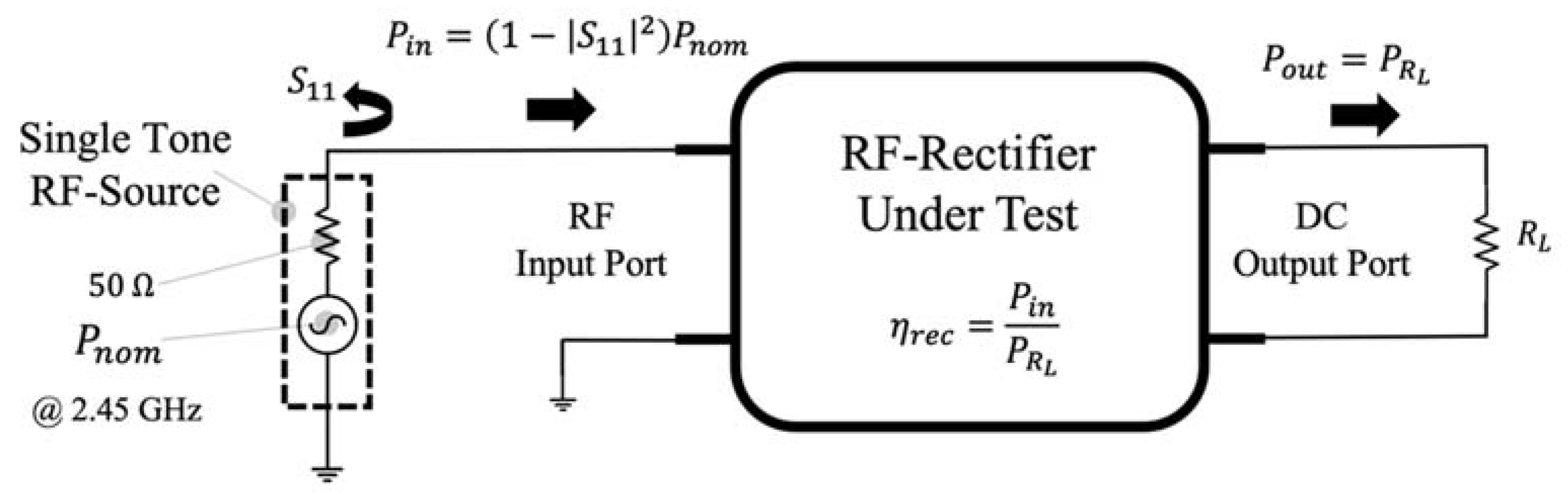
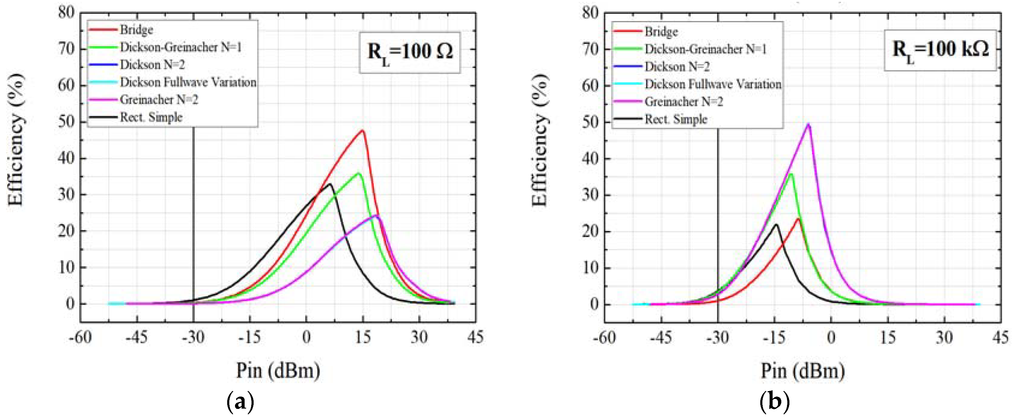
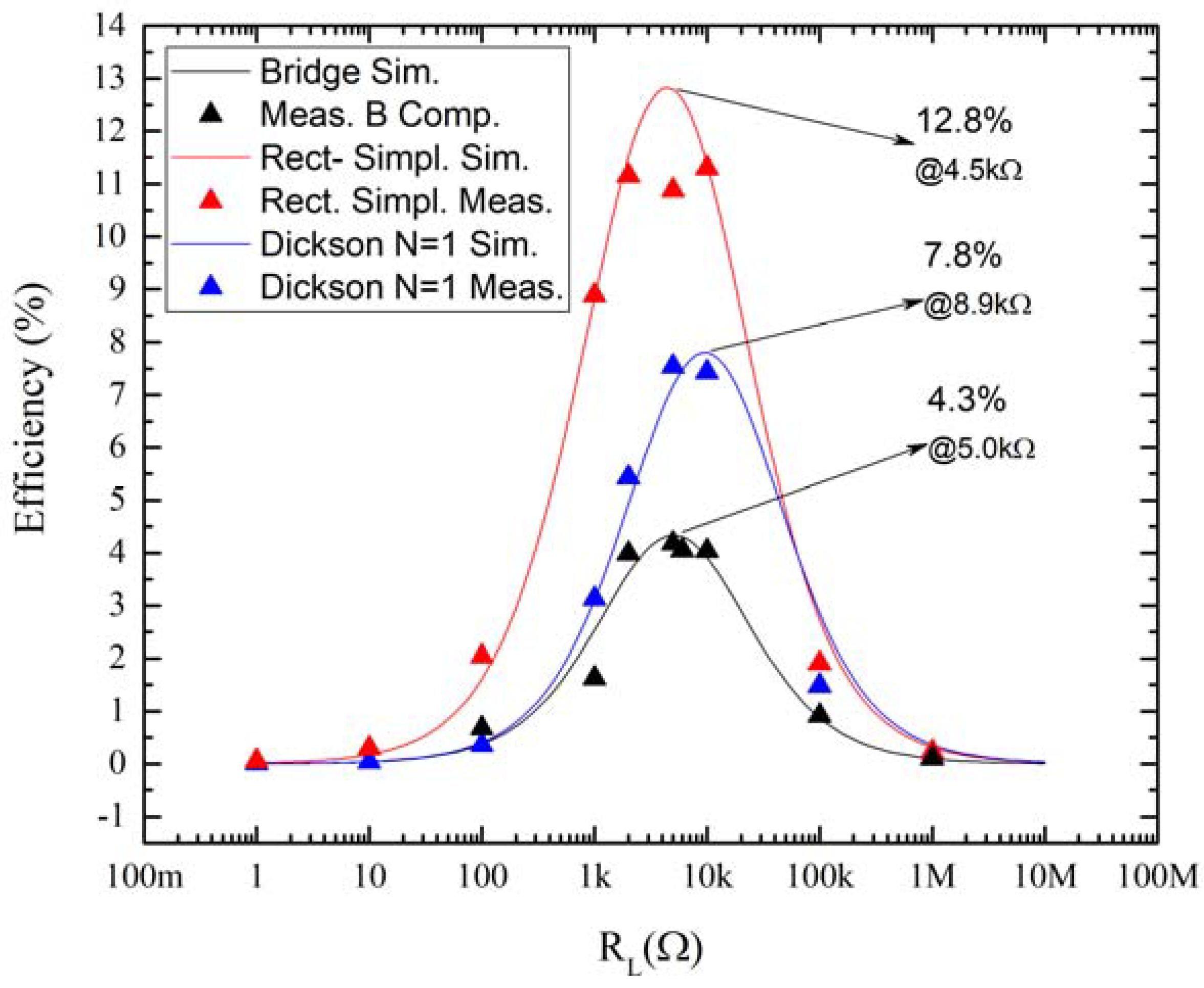
3. Parametric Analysis of RF Rectifier Circuits Efficiency
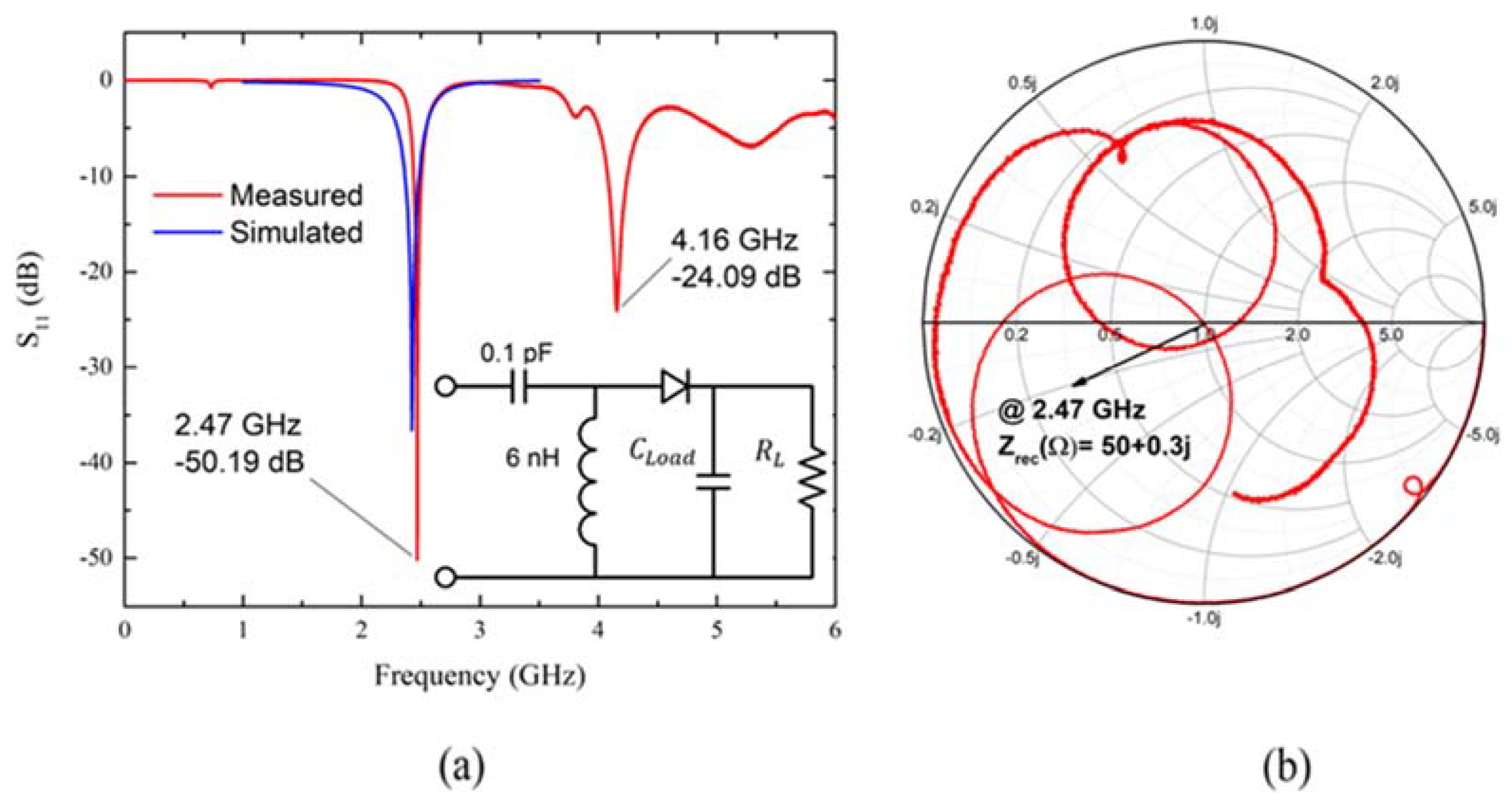
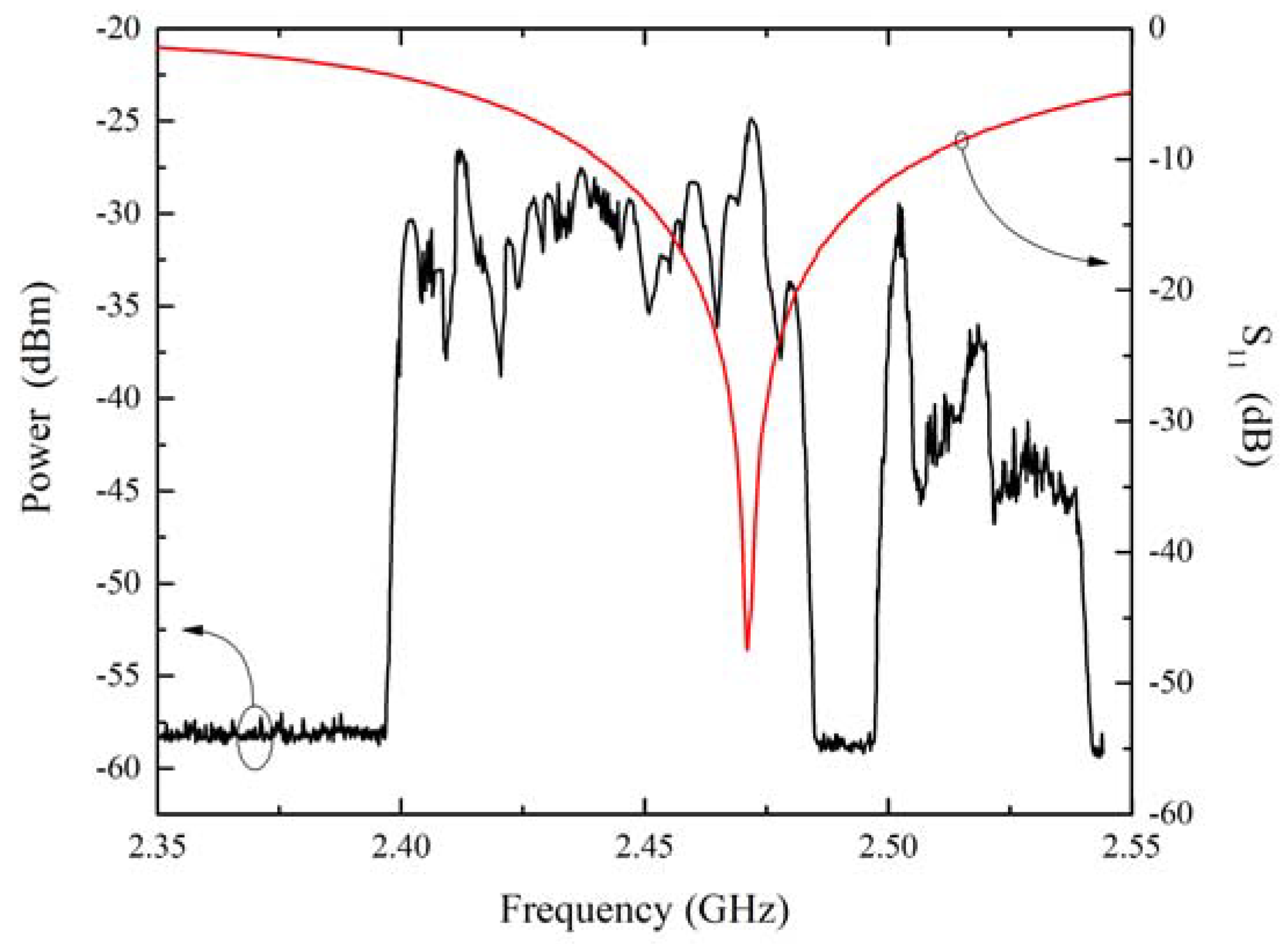
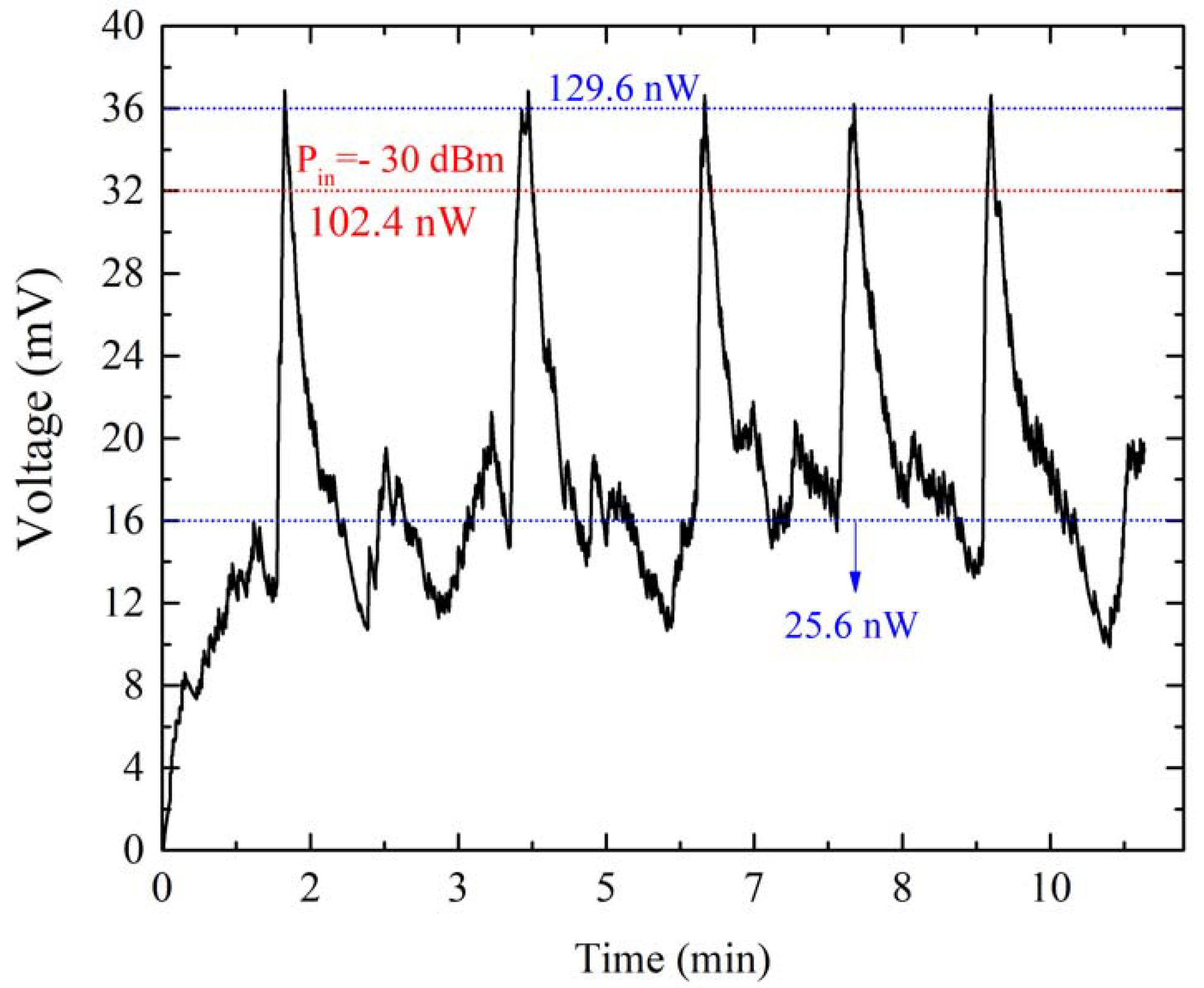
4. Ambient RF Energy Harvesting Prototype Performance in Real Conditions
5. Conclusions
Funding
Institutional Review Board Statement
Informed Consent Statement
Data Availability Statement
Conflicts of Interest
References
- Cansiz, M.; Altinel, D.; Kurt, G.K. Efficiency in RF energy harvesting systems: A comprehensive review. Energy 2019, 174, 292–309. [Google Scholar] [CrossRef]
- PowerCast. P2110-915 MHz RF Powerharvester Receiver Data Sheet. 2018. Available online: https://www.powercastco.com/ (accessed on 1 July 2022).
- Finnegan, J.; Niotaki, K.; Brown, S. Exploring the boundaries of ambient rf energy harvesting with lorawan. IEEE Internet Things J. 2021, 8, 5736–5743. [Google Scholar] [CrossRef]
- Wagih, M.; Weddell, A.S.; Beeby, S. Millimeter-Wave Power Harvesting: A Review. IEEE Open J. Antennas Propag. 2020, 1, 560–578. [Google Scholar] [CrossRef]
- Luo, Y.; Pu, L.; Wang, G.; Zhao, Y. RF energy harvesting wireless communications: Rf environment, device hardware and practical issues. Sensors 2019, 19, 3010. [Google Scholar] [CrossRef] [PubMed] [Green Version]
- Jayakody, D.N.K.; Thompson, J.; Chatzinotas, S.; Durrani, S. Wireless Information and Power Transfer: A New Paradigm for Green Communications; Springer International Publishing: Cham, Switzerland, 2017. [Google Scholar]
- Gu, X.; Grauwin, L.; Dousset, D.; Hemour, S.; Wu, K. Dynamic Ambient RF Energy Density Measurements of Montreal for Battery-Free IoT Sensor Network Planning. IEEE Internet Things J. 2021, 8, 13209–13221. [Google Scholar] [CrossRef]
- Kim, S.; Vyas, R.; Bito, J.; Niotaki, K.; Collado, A.; Georgiadis, A.; Tentzeris, M.M. Ambient RF energy-harvesting technologies for self-sustainable standalone wireless sensor platforms. Proc. IEEE 2014, 102, 1649–1666. [Google Scholar] [CrossRef]
- Luo, Y.; Pu, L. Practical Issues of Energy Harvesting and Data Transmissions in Sustainable IoT. arXiv 2019. [Google Scholar] [CrossRef]
- Peruzzi, G.; Pozzebon, A. A review of energy harvesting techniques for low power wide area networks (LPWANs). Energies 2020, 13, 3433. [Google Scholar] [CrossRef]
- Raza, U.; Salam, A. On-site and external energy harvesting in underground wireless. Electronics 2020, 9, 681. [Google Scholar] [CrossRef] [Green Version]
- Muncuk, U.; Alemdar, K.; Sarode, J.D.; Chowdhury, K.R. Multiband ambient RF energy harvesting circuit design for enabling batteryless sensors and IoT. IEEE Internet Things J. 2018, 5, 2700–2714. [Google Scholar] [CrossRef]
- Pinuela, M.; Mitcheson, P.D.; Lucyszyn, S. Ambient RF energy harvesting in urban and semi-urban environments. IEEE Trans. Microw. Theory Tech. 2013, 61, 2715–2726. [Google Scholar] [CrossRef]
- Yang, L.; Zhou, Y.J.; Zhang, C.; Yang, X.M.; Yang, X.-X.; Tan, C. Compact Multiband Wireless Energy Harvesting Based Battery-Free Body Area Networks Sensor for Mobile Healthcare. IEEE J. Electromagn. RF Microwaves Med. Biol. 2018, 2, 109–115. [Google Scholar] [CrossRef]
- Coskuner, E.; Garcia-Garcia, J. Metamaterial impedance matching network for ambient rf-energy harvesting operating at 2.4 GHz and 5 GHz. Electronics 2021, 10, 1196. [Google Scholar] [CrossRef]
- Vandelle, E.; Bui, D.H.N.; Vuong, T.-P.; Ardila, G.; Wu, K.; Hemour, S. Harvesting Ambient RF Energy Efficiently with Optimal Angular Coverage. IEEE Trans. Antennas Propag. 2019, 67, 1862–1873. [Google Scholar] [CrossRef]
- Hu, Y.-Y.; Sun, S.; Xu, H.; Sun, H. Grid-Array Rectenna with Wide Angle Coverage for Effectively Harvesting RF Energy of Low Power Density. IEEE Trans. Microw. Theory Tech. 2019, 67, 402–413. [Google Scholar] [CrossRef]
- Palazzi, V.; Kalialakis, C.; Alimenti, F.; Mezzanotte, P.; Roselli, L.; Collado, A.; Georgiadis, A. Design of a ultra-compact low-power rectenna in paper substrate for energy harvesting in the Wi-Fi band. In Proceedings of the 2016 IEEE Wireless Power Transfer Conference (WPTC), Aveiro, Portugal, 5–6 May 2016; pp. 23–26. [Google Scholar] [CrossRef]
- Karampatea, A.; Siakavara, K. Synthesis of rectenna for powering micro-watt sensors by harvesting ambient RF signals’ power. Electronics 2019, 8, 1108. [Google Scholar] [CrossRef] [Green Version]
- Karampatea, A.; Siakavara, K. Hybrid rectennas of printed dipole type on Double Negative Dielectric Media for powering sensors via RF ambient energy harvesting. AEU-Int. J. Electron. Commun. 2019, 108, 242–250. [Google Scholar] [CrossRef]
- Chang, Y.; Zhang, P.; Wang, L. Highly efficient differential rectenna for RF energy harvesting. Microw. Opt. Technol. Lett. 2019, 61, 2662–2668. [Google Scholar] [CrossRef]
- Song, C.; Huang, Y.; Carter, P.; Zhou, J.; Joseph, S.D.; Li, G. Novel Compact and Broadband Frequency-Selectable Rectennas for a Wide Input-Power and Load Impedance Range. IEEE Trans. Antennas Propag. 2018, 66, 3306–3316. [Google Scholar] [CrossRef]
- Li, P.; Long, Z.; Yang, Z. RF Energy Harvesting for Batteryless and Maintenance-Free Condition Monitoring of Railway Tracks. IEEE Internet Things J. 2021, 8, 3512–3523. [Google Scholar] [CrossRef]
- Marshall, B.R.; Morys, M.M.; Durgin, G.D. Parametric analysis and design guidelines of RF-to-DC Dickson charge pumps for RFID energy harvesting. In Proceedings of the 2015 IEEE International Conference on RFID (RFID), San Diego, CA, USA, 15–17 April 2015; pp. 32–39. [Google Scholar] [CrossRef]
- Cheng, L.W.; Gnanagurunathan, G. Two-Stage Dickson Charge Pump Rectifier with Harmonics Suppression for 2.45 GHz WPT. In Proceedings of the 2020 IEEE International RF and Microwave Conference (RFM), Kuala Lumpur, Malaysia, 14–16 December 2020; pp. 15–18. [Google Scholar] [CrossRef]
- Fan, S.; Yuan, Z.; Gou, W.; Member, S.; Zhao, Y. A 2.45-GHz Rectifier-Booster Regulator With Impedance Matching Converters for Wireless Energy Harvesting Shiquan. IEEE Trans. Microw. Theory Tech. 2019, 67, 3833–3843. [Google Scholar] [CrossRef]
- Berges, R.; Fadel, L.; Oyhenart, L.; Vigneras, V.; Taris, T. Conformable dual-band wireless energy harvester dedicated to the urban environment. Microw. Opt. Technol. Lett. 2020, 62, 3391–3400. [Google Scholar] [CrossRef]
- Curty, J.-P.; Joehl, N.; Krummenacher, F.; Dehollain, C.; Declercq, M.J. A model for μ-power rectifier analysis and design. IEEE Trans. Circuits Syst. I Regul. Pap. 2005, 52, 2771–2779. [Google Scholar] [CrossRef]
- Chandravanshi, S.; Akhtar, M.J. An efficient dual-band rectenna using symmetrical rectifying circuit and slotted monopole antenna array. Int. J. RF Microw. Comput. Eng. 2020, 30, e22117. [Google Scholar] [CrossRef]
- Song, C.; Huang, Y.; Zhou, J.; Zhang, J.; Yuan, S.; Carter, P. A high-efficiency broadband rectenna for ambient wireless energy harvesting. IEEE Trans. Antennas Propag. 2015, 63, 3486–3495. [Google Scholar] [CrossRef] [Green Version]
- Zhang, H.; Zhong, Z.; Guo, Y.-X.; Wu, W. Differentially-fed charge pumping rectifier design with an enhanced efficiency for ambient RF energy harvesting. In Proceedings of the 2017 IEEE MTT-S International Microwave Symposium (IMS), Honololu, HI, USA, 4–9 June 2017; pp. 613–616. [Google Scholar] [CrossRef]
- Valenta, C.R.; Durgin, G.D. Harvesting wireless power: Survey of energy-harvester conversion efficiency in far-field, wireless power transfer systems. IEEE Microw. Mag. 2014, 15, 108–120. [Google Scholar] [CrossRef]
- Skyworks Solutions. Surface Mount Mixer and Detector Schottky Diodes. Data Sheet. 2016. Available online: https://www.skyworksinc.com/-/media/A36775836A4E4BA8A92104088692424F.ashx (accessed on 1 March 2021).


| Ref. | Eff. | ||||
|---|---|---|---|---|---|
| Simple diode-capacitor rectifier | [16] | 45% |  | ||
| [17] | −6.6 dBm | 48% | |||
| [18] | −15 dBm | 28% | |||
| Four-diode Bridge | [15] | −30 dBm | 8.8% | 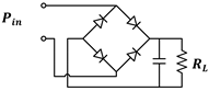 | |
| [19] | −9.2 dBm | 68% | |||
| [20] | −7.6 dBm | 58% | |||
| [21] | 17 dBm | 50% | |||
| Dickson-Greinacher N = 1 | [22] | −20 dBm | 5% | 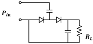 | |
| [23] | −15 dBm | 20% | |||
| [24] | −20 dBm | 17% | |||
| Dickson | [23] | −5 dBm | 70% | 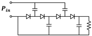 | |
| [25] | 5 dBm | 59% | |||
| [24] | −20 dBm | 5% | |||
| Greinacher | [26] | 13 dBm | 37.5% | 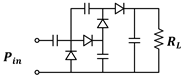 | |
| [27] | −5 dBm | 10% | |||
| [28] | −7.5 dBm | 9% | |||
| Full-Wave Dickson Variation | [29] | 9 dBm | 68% | 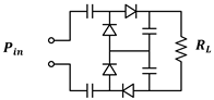 | |
| [27] | −20 dBm | 6% | |||
| [30] | −27.5 dBm | 5% | |||
| [31] | −20 dBm | 12% |
| Frequential Component | ||||||
|---|---|---|---|---|---|---|
| Fourier Coefficient | Output Power Coefficient | Input Power Percentage | Fourier Coefficient | Output Power Coefficient | Input Power Percentage | |
| DC | 67% | 64% | ||||
| -- | -- | |||||
| 15% | 30% | |||||
| -- | -- | -- | -- | -- | -- | |
| 3% | 6% | |||||
Publisher’s Note: MDPI stays neutral with regard to jurisdictional claims in published maps and institutional affiliations. |
© 2022 by the author. Licensee MDPI, Basel, Switzerland. This article is an open access article distributed under the terms and conditions of the Creative Commons Attribution (CC BY) license (https://creativecommons.org/licenses/by/4.0/).
Share and Cite
Garcia-Garcia, J.J. Considerations for the Design and Implementation of Ambient RF Signal Rectifiers in the 2.45 GHz WiFi Band. Appl. Sci. 2022, 12, 7884. https://doi.org/10.3390/app12157884
Garcia-Garcia JJ. Considerations for the Design and Implementation of Ambient RF Signal Rectifiers in the 2.45 GHz WiFi Band. Applied Sciences. 2022; 12(15):7884. https://doi.org/10.3390/app12157884
Chicago/Turabian StyleGarcia-Garcia, Joan J. 2022. "Considerations for the Design and Implementation of Ambient RF Signal Rectifiers in the 2.45 GHz WiFi Band" Applied Sciences 12, no. 15: 7884. https://doi.org/10.3390/app12157884
APA StyleGarcia-Garcia, J. J. (2022). Considerations for the Design and Implementation of Ambient RF Signal Rectifiers in the 2.45 GHz WiFi Band. Applied Sciences, 12(15), 7884. https://doi.org/10.3390/app12157884