1. Introduction
Due to the advantages of high power density, competitive low cost, and multi-port interconnection, the three-port isolated dc-dc converter has emerged as an attractive solution to construct future renewable energy systems, such as the micro-grid, hybrid energy storage systems, electrical vehicles, etc. [
1,
2,
3].
According to the number of transformer winding, the existing isolated three-port dc-dc converters mainly include the single-transformer type and the two-transformer type [
4,
5,
6,
7,
8,
9,
10,
11,
12,
13,
14]. The single-transformer converter presents a clear advantage regarding the increase of the power density and the system integration. The popular single-transformer three-port converter is the triple-active-bridge (TAB) converter, which consists mainly of two types: inductor-based and resonant-based. For the inductor-type topology, the leakage inductor and external inductor of the transformer winding are used to store energy and transfer power. For the resonant-type topology, resonant tanks are used to transfer power. Combining the principle of this type of converter, the shape of the transformer current of the resonant-type is close to the sinusoidal. The current stress of the resonant-type is significantly lower than that of the inductor-type. Hence, the resonant-type has a better electromagnetic characteristic and low current stress as compared with the inductor-type [
15,
16,
17]. The resonant-type increases operating efficiency and the utilization rate of the system hardware rated capacity.
The TAB dc-dc converter realizes the galvanic isolation by using the three-winding transformer. The magnetic coupling of the transformer will cause the power coupling among the three ports of the converter. This results in the various ports not being able to transfer power independently and precisely. The existing power decoupling strategies mainly include the topology-level and the control-level ones. In [
18], the resonant tanks are added to the TAB converter, then the degree of power coupling is decreased by reducing the proportion of the switching frequency to the resonant frequency. This method cannot completely eliminate power coupling. In addition, the current stress will increase when the resonant frequency is different from the switching frequency. In [
19], an isolated three-port converter is proposed. The decoupling resonant tank is added to the battery port, which results in the power flow between the PV port and dc-bus port being transferred indirectly via the battery port. This increases additional power loss. In [
20,
21], the decoupling matrix is applied to the control loop to compensate for the coupling between the control variables, then realizes the independent control of the transfer power. The solution of the decoupling matrix depends on the small-signal model of the converter. Thus, the universality of the decoupling network is not very good. Meanwhile, the complexity of the control system is still the challenge of the decoupling strategy at the control level.
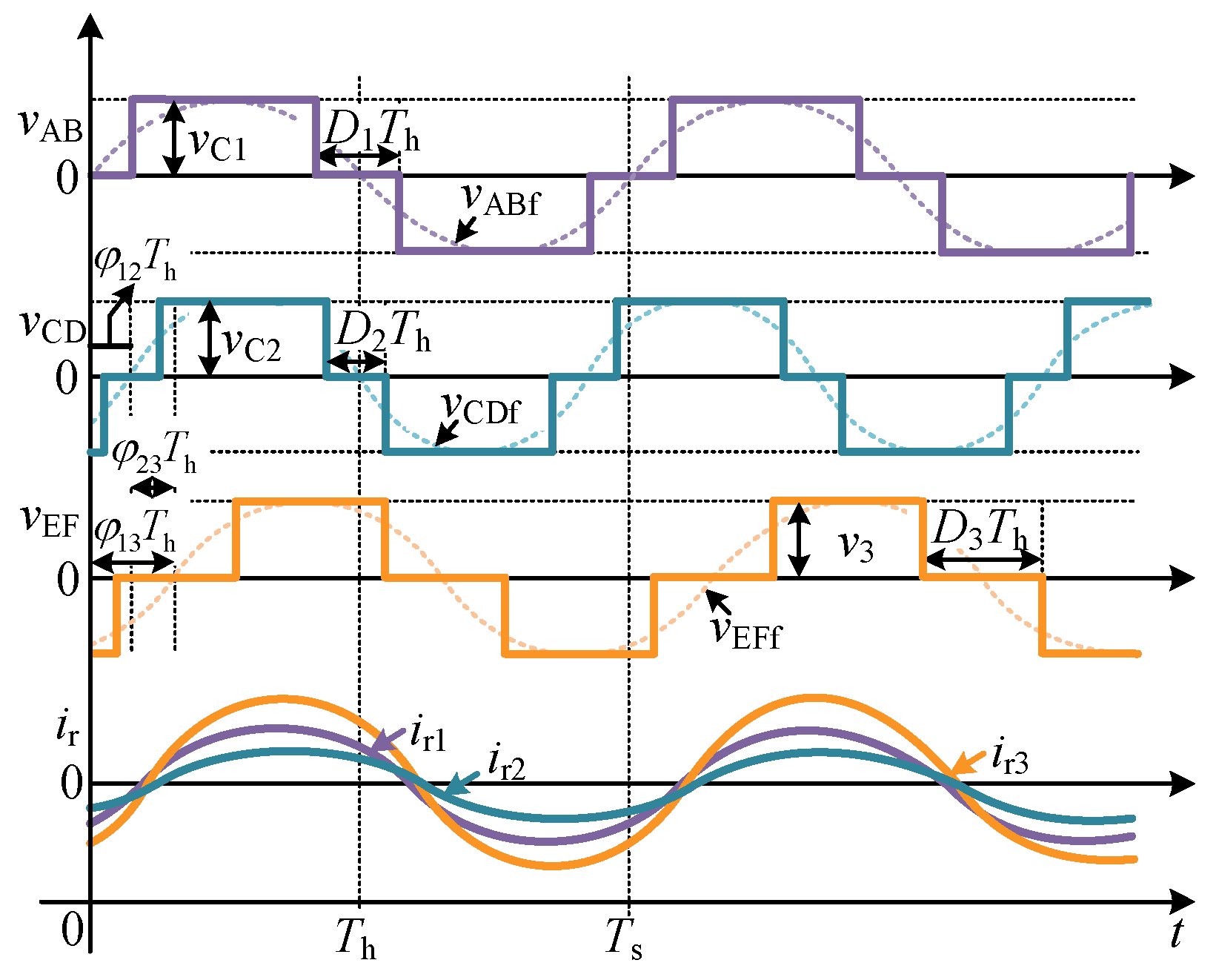
Up to now, the single-phase-shift (SPS) modulation is widely used in the TAB converter [
22,
23]. In SPS modulation, the internal phase-shift angle of the three ports is fixed to 0, only the external phase-shift angle is used to control the magnitude and direction of the transfer power. This modulation is easy to realize. However, there are no other control variables to further optimize the performance of the three-port converter. When the voltage magnitude of the windings of the transformer is not matched, the RMS value and peak value of the transformer current are greatly increased. The power loss becomes much higher and the efficiency is greatly reduced.
The better performance of the converter is realized by increasing the controllable degree of freedom. In a dual-active-bridge converter, the optimization control of the transformer current, reactive power, and power loss is realized by adjusting the relationship between the control variables, thereby improving the operational efficiency of the converter. While the structural coupling of the three-port converter causes the control variables of each port to be interactive. The two equivalent two-port converters are likely to have different optimal operating points of the control variables on the common port when the range of the voltage and transfer power is different. Hence, it is important to propose a unified global optimization modulation based on the multiple controllable variables. It is helpful to reduce power loss and increase efficiency.
In this paper, a topology-level power decoupling TAB converter and its optimized multi-phase-shift modulation are proposed. The innovation and contribution are below. (1) In terms of the topology, a topology-level power decoupling TAB isolated resonant dc-dc converter is proposed in this paper. A resonant capacitor is added to the three-winding transformer to realize the power decoupling at the topology level. The converter realizes the power decoupling only by setting the hardware parameters and without adding an additional controller. Hence, the decoupling effect of the converter is improved and the complexity of the control system is significantly reduced. (2) Meanwhile, different from the inductor-type topology, the energy storage component of the proposed converter is the series-resonant tank, which significantly reduces the current stress and increases the utilization rate of the hardware. (3) In terms of the modulation, the existing TAB converters generally use the single-phase-shift modulation. In this paper, the optimized multi-phase-shift modulation for the TAB converter is proposed. With the increase of the controllable degree of freedom, the performance of the converter is correspondingly improved. On this basis, the RMS value of the transformer current is minimized and the power loss in the entire voltage and power range is accordingly reduced, thus ensuring the high efficiency of the converter.
3. Global Optimization of Multiple Phase Shifts to Minimize Ohmic Loss
For the converter, besides realizing the real-time adjustment of the transfer power, one important aspect is to reduce the power loss. In theory, there are five phase shifts that can be used to adjust the transfer power. In this section, reducing the power loss and increasing the operating efficiency in the entire voltage and power range are used as the objective to optimize the multi-phase-shift modulation. In addition, the soft-switching performance is analyzed.
The power loss of the converter mainly includes the switching loss
Psw, the conduction loss
Pcond, the copper loss
Pcopp, the iron loss
Piron, and so on. Combined with the theoretical analysis and the distribution diagram of the power loss in [
24], both
Pcond and
Pcopp are positively correlated with the square of the RMS value of the transformer current, thus, they are collectively called the ohmic loss
Pohm.
Pohm has a high proportion of the total power loss in the entire power range. As the transfer power and the transformer current increase, the proportion of
Pohm increases accordingly. Hence, reducing
Pohm is effective to improve the converter efficiency.
Pohm,
Pcond, and
Pcopp are respectively calculated as
where
RDS1,
RDS2, and
RDS3 respectively denote the on-state resistance of the power switches of each port.
Rtran1,
Rtran2, and
Rtran3 respectively denote the resistance of the transformer windings of each port.
Ir1f,rms,
Ir2f,rms, and
Ir3f,rms respectively denote the RMS value of the fundamental component of the transformer current of each port.
From (13)–(15), Pohm is closely related to Ir1f,rms, Ir2f,rms, and Ir3f,rms. The smaller the RMS value of the transformer current is, the smaller the ohmic loss will be. Therefore, the optimization objective of the modulation is equivalent to minimizing the RMS value of the transformer current.
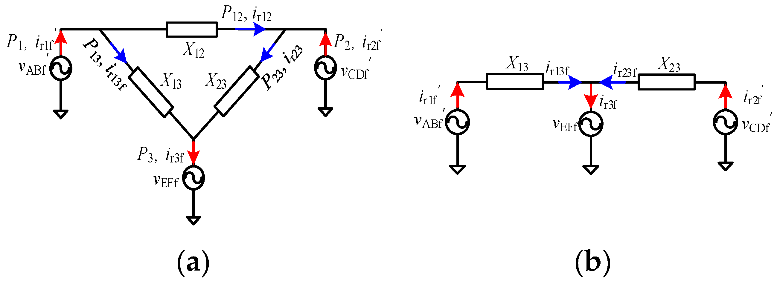
After the power is decoupled between port 1 and port 2,
ir1f =
ir13f, and
ir2f =
ir23f, hence, combining (6) and (7),
Ir1f,rms, and
Ir2f,rms are calculated as
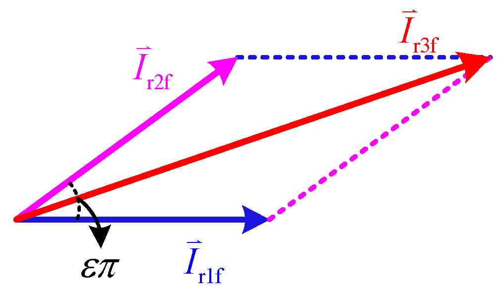
The fundamental component of ir3f is composed of
ir1f and
ir2f. The relationship of the phasors
,
and
of the transformer current
ir1f,
ir2f, and
ir3f is shown in
Figure 4, where ε is the phase difference between
and
.
Ir1f,rms,
Ir2f,rms, and
Ir3f,rms are the magnitude of the phasors
,
and
, respectively. Hence,
Ir3f,rms is calculated as
From (18), under the same transfer power, when
Ir1f,rms, and
Ir2f,rms are both the minimum,
Ir3f,rms is also the minimum. Therefore, the functions of the optimization objective are expressed as
where
G13 and
,
G23 and
are the index of the actual and desired transfer power of port 1 and port 2, respectively.
G13 and
G23 are respectively expressed as
Since port 3 is the common port of the two equivalent two-port converter and
D3 is determined by the operating state of both port 1 and port 2, the optimal operating point of
D3 is analyzed at first. Combining (3), (16), and (17), the average transfer power of port 1 and port 2 are respectively calculated and expressed as
where
VEFf,rms is the RMS value of
vEFf.
θ1 is the phase difference between
vEFf and
ir1f.
θ2 is the phase difference between
vEFf and
ir2f.
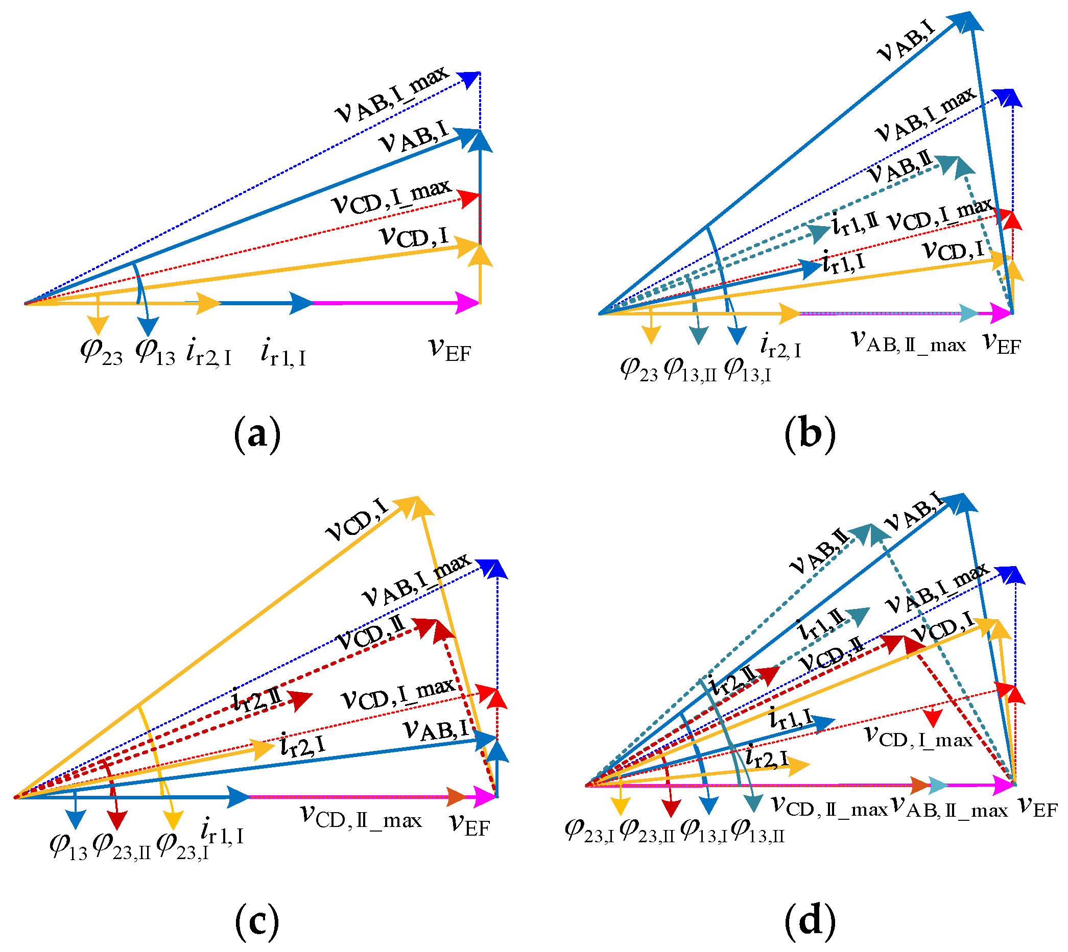
From (23) and (24), under the same transfer power, the smaller D3 is, the smaller Ir1f,rms, and Ir2f,rms will be. Therefore, D3 is always set to 0 under the proposed modulation to minimize the transformer current. On this basis, the KKT conditions based on the Lagrange multiplier method are used to solve the nonlinear optimization problem shown in (19) and (20). According to the range of voltage gain and the transfer power, the optimization results include the following four states and are expressed as (25), (32), (34), and (36).
Furthermore, it is useful to construct the phasor diagram of the fundamental equivalent converter to verify the principle of the optimization strategy in the time domain. The optimization results of the four states and the corresponding phasor diagrams are described as follows.
State 1: when
,
,
and
, the optimization result is expressed as
Substituting (25) into (1)–(3), the voltage phasors of the fundamental equivalent converter satisfy
Thus, the phasor diagram is shown in
Figure 5a. It can be seen that ir1f and ir2f are always in a phase of vEFf in this state. Both the equivalent two-port converters operate at the unity power factor. Hence, the RMS value of the transformer current is the smallest. As the transfer power increases,
D1,
D2,
and
vary accordingly. It ensures
ir1f and
ir2f are always in a phase of
vEFf, that is, the converter operates at the minimum RMS value of the transformer current. In this state, the per-unit transfer power of port 1 and 2 are simplified and expressed as
The soft-switching conditions of this state are analyzed as follows. Combining the analysis of the soft-switching principle in [
25], the ZV off is realized naturally. The ZV on is achieved by gating on the in-coming power switch while the anti-parallel diode is conducting. Hence, take port 1 as an example, the ZV-on conditions of the switches are expressed as
Substituting (5) into (29), the ZV-on conditions of the switches on port 1 are expressed as
Similarly, substituting (6) into (29), the ZV-on conditions of the switches on port 2 are expressed as
Meanwhile, since ir3 is always in a phase of vEF in this state, the ZC on is always achieved and independent of the topology parameters for all the switches on port 3.
State 2: when
,
,
and
or
,
and
. The optimization result is expressed as
The phasor diagram is shown in
Figure 5b. In this state, the range of the voltage gain and transfer power between port 2 and port 3 is the same as that of state 1. According to the range of
k1, there are two cases of state 2:
k1 < 1 and
. They are represented by “I” and “II” in
Figure 5b. In both cases, the relationship between the phase shifts of port 1 and
G13* is the same. The modulation of port 1 is simplified to SPS modulation, while there are some differences in the physical interpretation of the two cases.
(1) Case I (k1 < 1): As G13* increases, D1 reduces to 0, and the magnitude of vABf increases to the maximum value vABf,I_max. Since the smaller the phase difference between ir1 and vEF, the smaller the reactive power component and the RMS value of the transformer current. As G13* continues to increase, the magnitude of vABf remains at vABf,I_max to minimize the phase difference between ir1 and vEF. On this basis, the transfer power is only controlled by .
(2) Case II (): The magnitude of vABf is always smaller than that of vEFf in this case, thus there must be a phase difference between ir1f and vEFf. In order to minimize the phase difference between ir1 and vEF, the magnitude of vABf remains at the maximum value vABf,II_max in the entire power range.
In both cases, the modulation of port 1 is simplified to SPS modulation. The corresponding soft-switching operation conditions have been analyzed in detail in [
15]. The ZV-on condition of port 1 is expressed as
The operation state of port 2 is the same as that of state 1, hence, the ZV-on condition of port 2 is the same as (31).
For port 3, since the transformer currents of port 1 and port 2 are not in phase, it is difficult to get the analytical solution of
ir3. Combing the analysis in [
15], the ZV-on condition is
.
is the lagging angle between
ir3 and
vAB.
State 3: when
,
,
and
or
,
and
, the optimization result is expressed as
The phasor diagram is shown in
Figure 5c. In this state, the range of the voltage gain and transfer power between port 1 and port 3 is the same as that of state 1. According to the range of
k2, there are two cases of state 3:
and
. They are represented by “I” and “II” in
Figure 5c. The physical interpretation of the two cases is similar to that of state 2, thus no detailed description is given here.
The soft-switching performance of this state is similar to that of state 2. The ZV-on condition of port 1 is the same as (30). The ZV-on condition of port 3 is
. The ZV-on condition of port 2 is expressed as
State 4: when
,
,
and
or
and
, the optimization result is expressed as
The phasor diagram is shown in
Figure 5d. In this state, according to the range of
k1 and
k2, there are two cases of state 4. In both cases, the modulation strategies of port 1 and port 2 are simplified to SPS modulation.
(1) Case I ( and ): As G13* and G23* increase, both D1 and D2 reduce to 0. The magnitude of vABf and vCDf increases to the maximum value vABf,I_max, and vCDf,I_max. In order to reduce the RMS value of the transformer current, the magnitude of vABf remains at vABf,I_max, and the magnitude of vCDf remains at vCDf,I_max, as G13* continues to increase.
(2) Case II ( and ): The magnitude of vABf and vCDf are smaller than that of vEFf. Similarly, to minimize the RMS value of the transformer current, the magnitude of vABf and vCDf respectively remains at the maximum value vABf,II_max, and vCDf,II_max in the entire power range.
In this state, the modulation strategies of port 1 and port 2 are both simplified to SPS modulation. The ZV-on condition of port 1 and port 2 are expressed as (33) and (35), respectively. The ZV-on condition of port 3 is .
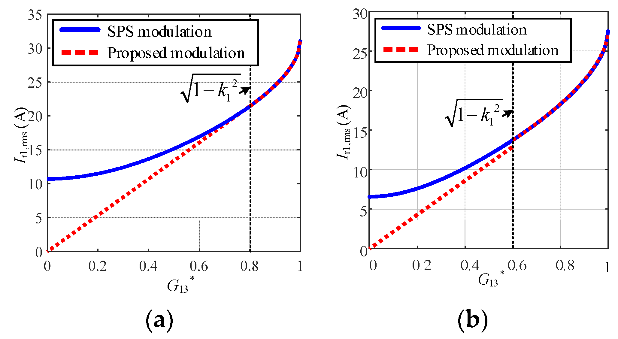
In order to verify the performance of the optimized multi-phase-shift modulation, the RMS value of the transformer current of the optimized modulation is contrasted with that of the traditional SPS modulation. It is obtained from (25), (32), (34), and (36) that the main difference between the proposed modulation and the SPS modulation lies in the range of
k1 < 1 and
k2 < 1. Taking port 1 as an example, the RMS values of the transformer current of the two modulations under
k1 < 1 are compared. The internal phase-shift angles of the three ports are all 0 under the SPS modulation, and the external phase-shift angles satisfy
The expressions (25), (32), and (36) are substituted into (16). The corresponding parameters are shown in
Table 1 and
k1 is set to 0.6 and 0.8. The distribution curves of
Ir1,rms as a function of the transfer power
G13* of the two modulation strategies are drawn in
Figure 6. It can be seen that the
Ir1,rms of the proposed strategy are significantly smaller than that of SPS modulation. In particular, as the voltage gain decreases, the advantage of the proposed modulation to reduce the RMS value of the transformer current is more obvious.
According to the above analysis, the proposed modulation realizes the global optimized control of the converter, as compared to the SPS modulation. The optimized modulation significantly reduces the RMS transformer current and the power loss. The converter efficiency is accordingly increased in the entire range of the voltage and transfer power.
4. Experimental Results and Analysis
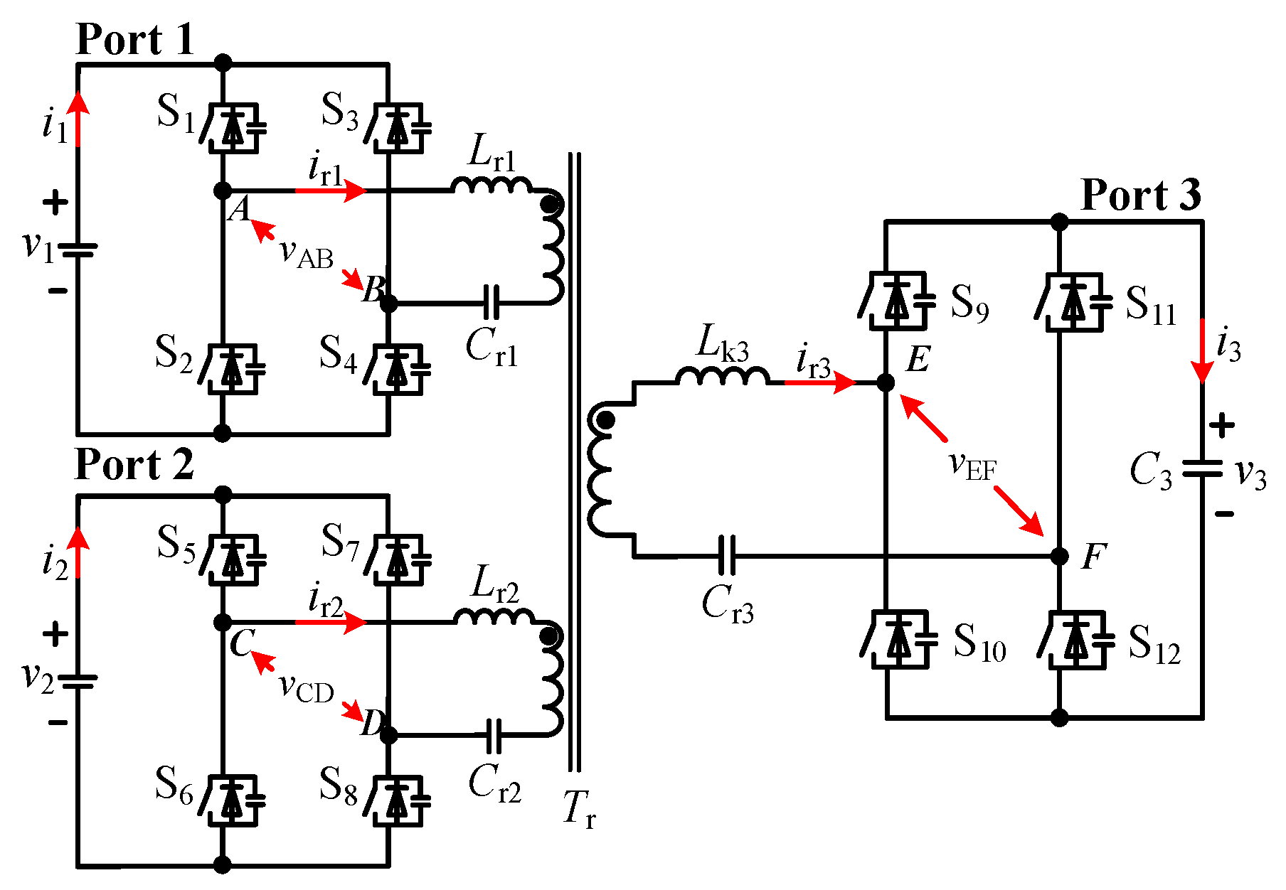
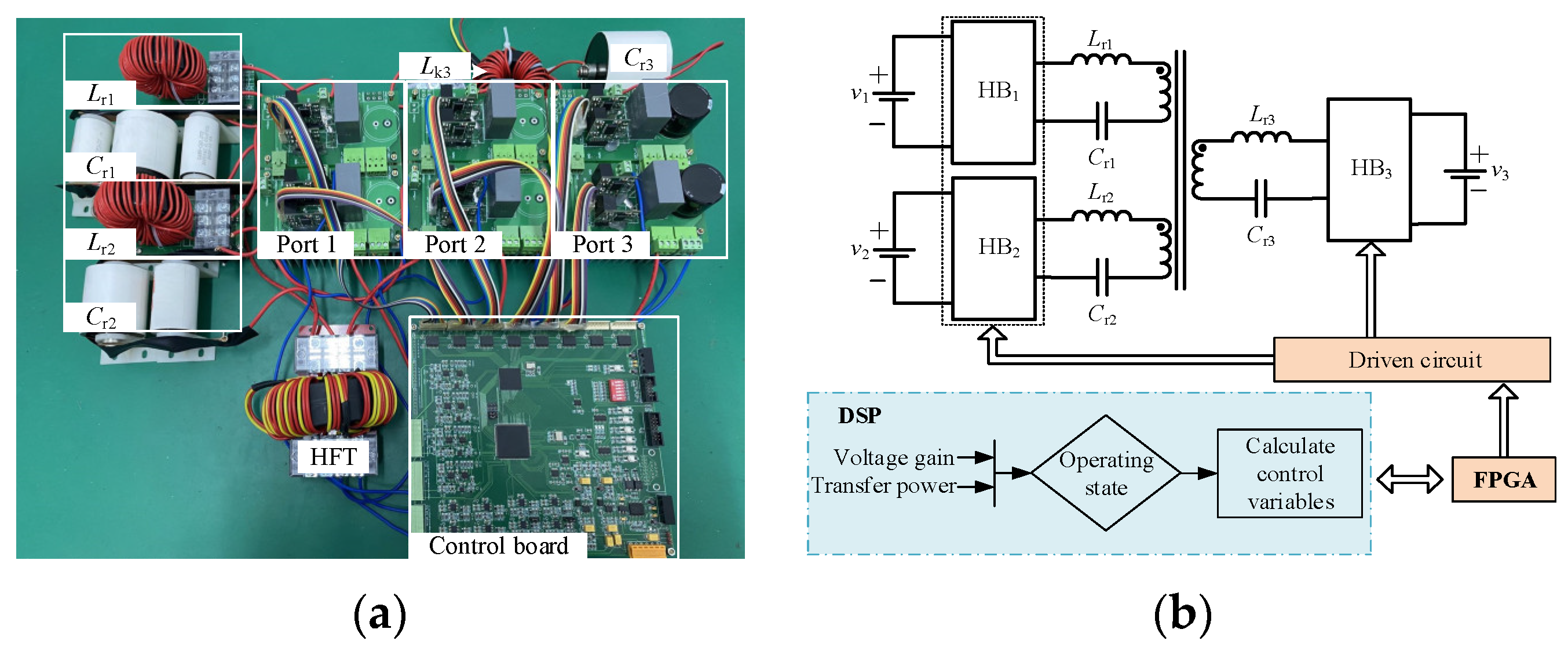
The proposed three-port converter and optimized modulation are verified by the built experimental platform shown in
Figure 7a. The modular approach is used to build the experimental platform. We have built some general half-bridge modules with the SiC power switches. The voltage rating of the switches is 650 V. Based on these modules, it is convenient to make up various dc-dc or dc-ac converters. Combining with the schematic of the proposed converter shown in
Figure 1, we use six modules to make up the proposed three-port converter in this experiment. Then combining with (4), (8), and (9) the parameters of the resonant tank of port 1 and port 2 are designed according to the requirements of the transmission power level. Combining with (4), (12) and the switching frequency
fs, the parameters of the resonant tank of port 3 are designed. The input inductors and bus capacitors of port 1 and port 2 are designed according to the ripple requirements of the input current and the bus voltage. In addition, three dc voltage sources and three resistors are connected in parallel to the three ports, respectively, so that the power can be transferred among the three ports under the bi-direction. The parameters of the experimental platform are listed in
Table 1. In order to verify the availability of the proposed modulation when the voltage gain varies in a wide range, the voltages on port 1 and 2 vary from 60 V to 150 V. In addition, to decrease the capacitance and rated voltage of the resonant capacitor used on port 3, an inductor is connected in series in the resonant tank. The total value of the leakage inductance of the transformer on port 3 and the external inductance is 101 μH. The three components construct the resonant tank with the resonant frequency of 50 kHz, which is equal to the switching frequency to realize the power decoupling. All experiments are performed under open-loop conditions. The control is implemented based on DSP + FPGA platform. The specific type of the used DSP and FPGA are TMS320F28377 and Cyclone IV, respectively. First, according to the range of voltage gain and transfer power, the operating state of the converter is selected. On this basis, the control variables are calculated, combined with (25), (32), (34), and (36). The above works are completed by DSP. Then, the calculations of DSP are transferred to FPGA and the driving signals of the switches are generated by FPGA. The block of the control configuration is shown in
Figure 7b.
According to power flowing direction, there are three types of operation modes, namely the forward mode, backward mode, and hybrid mode. In order to verify the performance of the power decoupling and the optimized modulation in the entire power range, the experimental results of various operation modes are all tested and analyzed separately below. As a comparison, the corresponding experimental results of the conventional TAB resonant converter without the decoupling resonant tank are also tested and shown here.
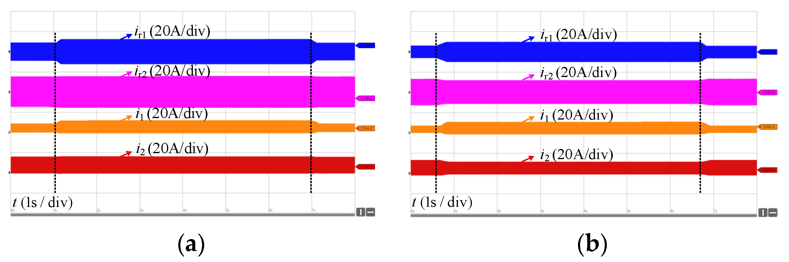
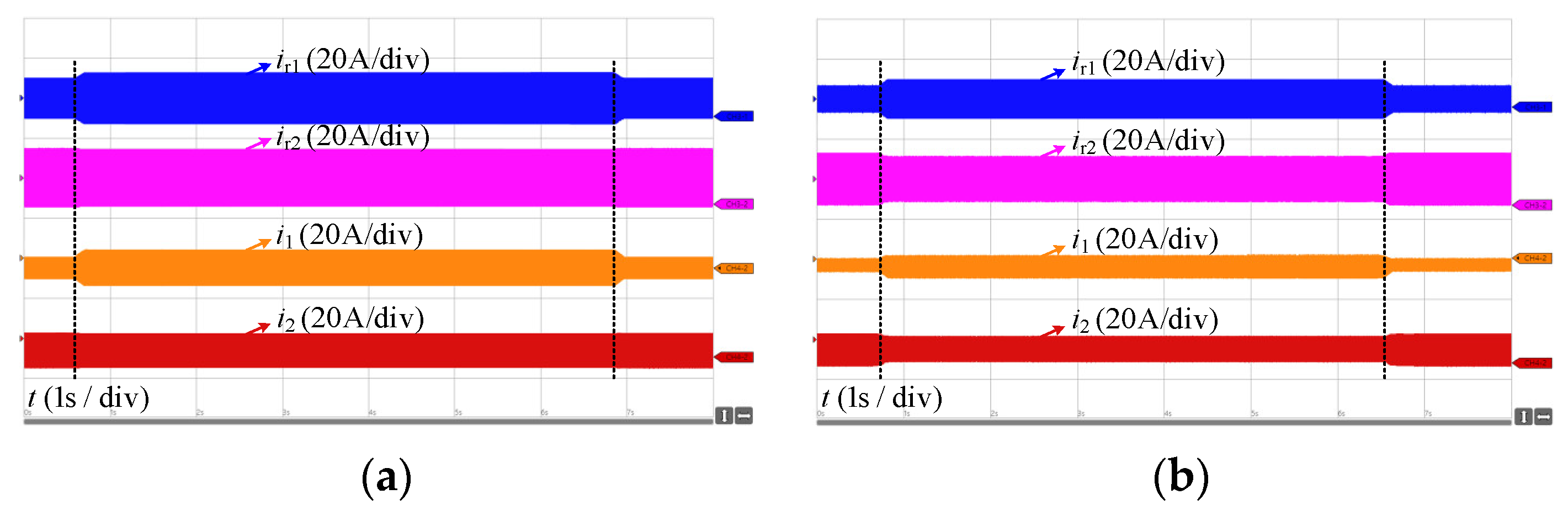
First, the performance of decoupling of both port 1 and port 2 operating in the forward mode is verified and compared with that of the conventional converter. In order to observe the performance of the power decoupling, the transfer power of port 2 remained constant and that of port 1 is stepped at some time. The corresponding experimental results of the converter and the conventional converter and the proposed one are shown in
Figure 8. From
Figure 8a, in the conventional converter, when
i1 step change occurs, the current of port 2
i2 varies accordingly.
This clearly reveals the power coupling problem. From
Figure 8b, in the proposed converter,
i2 keeps constant during the transient process, that is, the power coupling between port 1 and port 2 is eliminated.
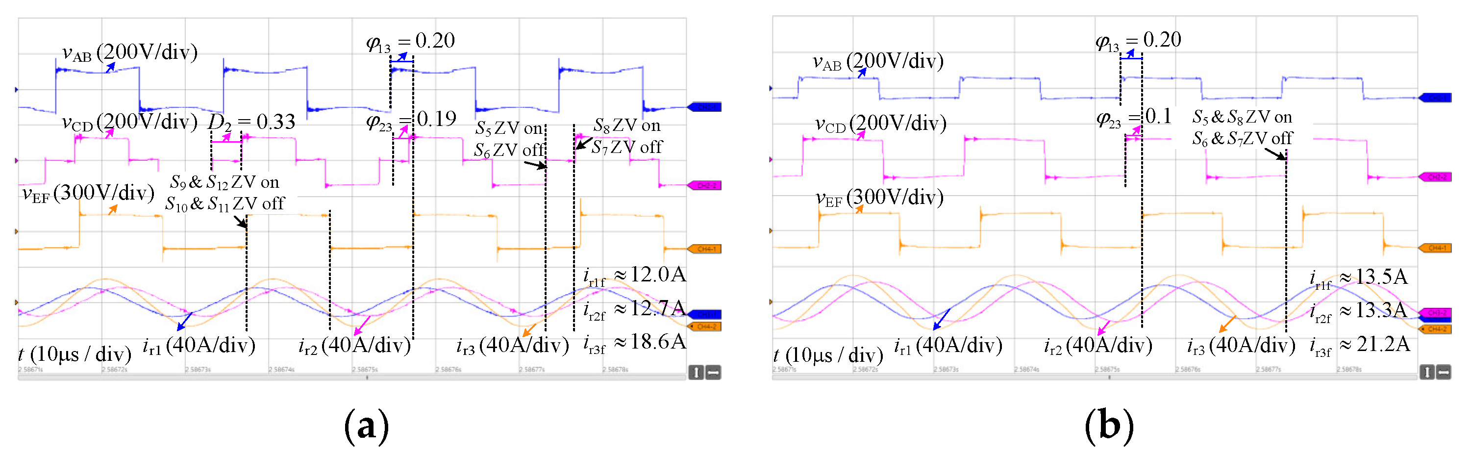
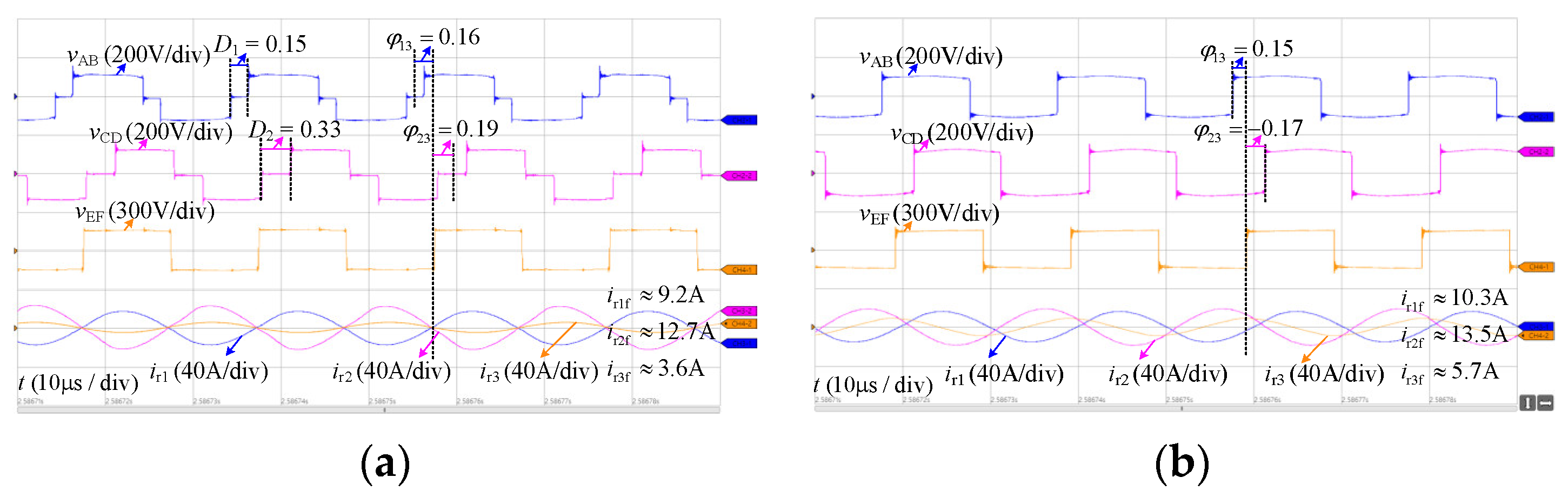
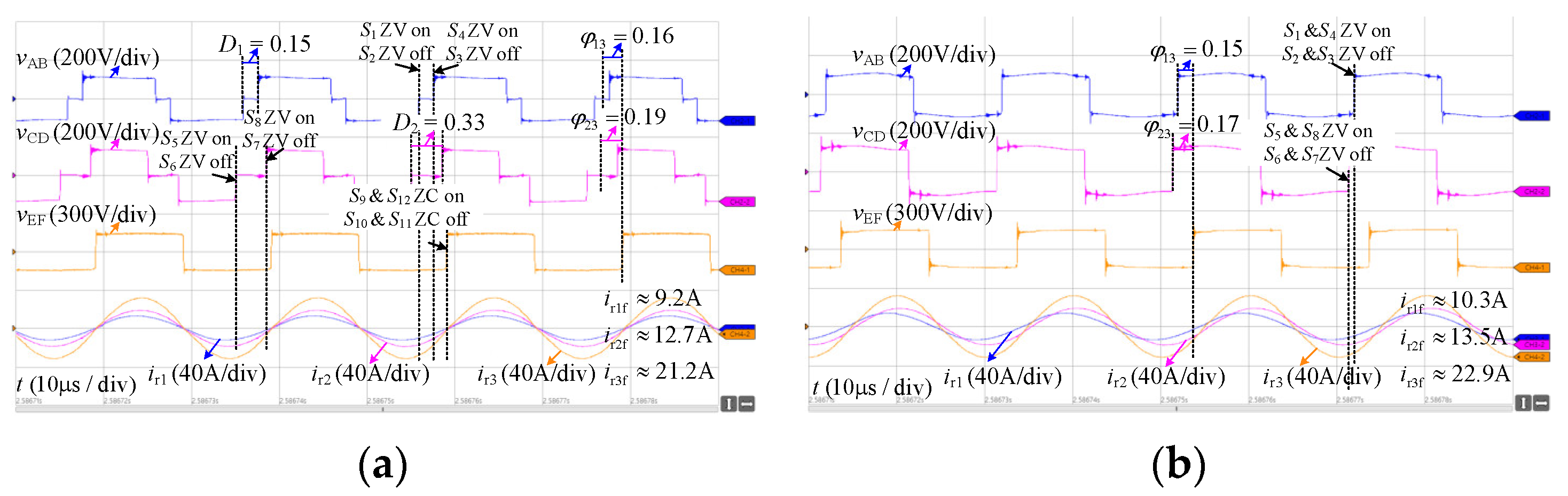
In the following, the global optimal modulation in all states is tested and compared with the SPS modulation. In state 1, the input voltages of port 1 and port 2 are set as 120 V and 140 V.
k1 and
k2 are accordingly 0.83 and 0.71. The corresponding experimental waveforms of state 1 with
P13 = 800 W and
P23 = 1 kW are shown in
Figure 9.
Figure 9a shows the experimental results of the optimized modulation.
D1,
D2,
and
calculated by the optimal conditions in (25) are 0.15, 0.33, 0.16, and 0.19, respectively.
ir1,
ir2, and
ir3 are all in a phase of
vEF. Hence, the converter operates at the minimum RMS value of the transformer current. In contrast, the experimental results of the SPS modulation under the same transfer power are shown in
Figure 9b. There is a phase difference between
ir1,
ir2,
ir3, and
vEF. The RMS value of the transformer current under the SPS modulation is greater than that of the optimized modulation. The experimental results verify under the same transfer power, the optimized modulation effectively reduces the RMS value of the transformer current, thereby reducing the power loss of the converter, compared with the SPS modulation. In addition, the power switching transition types are marked in the corresponding experimental results. All power switches of the three ports realize the soft-switching under the proposed modulation.
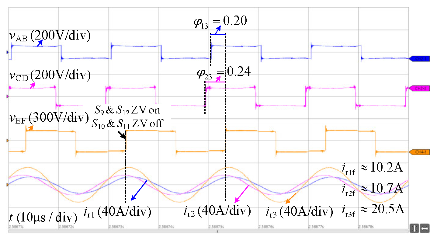
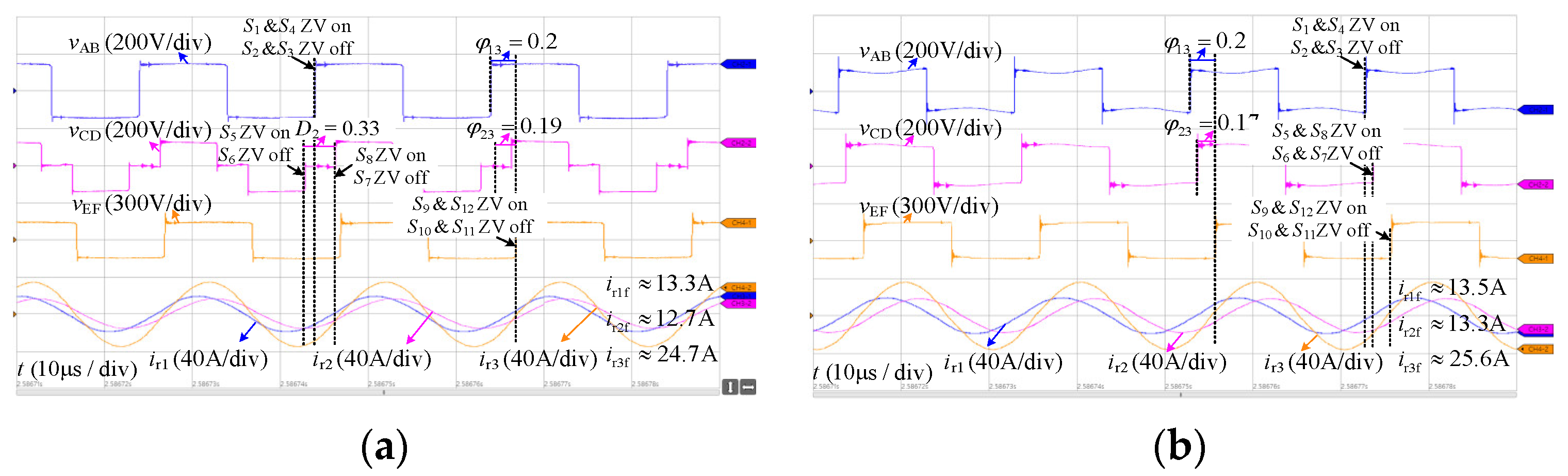
In state 2, there are two cases according to the range of
k1. First, the performance of the optimized modulation in the case of
k1 < 1 is tested. The transfer power of port 1 is set as 1kW.
Figure 10a,b show the experimental results of the optimized modulation and those of the SPS modulation, respectively.
D1,
D2,
, and
calculated by the optimal conditions in (27) are 0, 0.33, 0.2, and 0.19, respectively. It can be seen that, under the proposed modulation, port 2 operates at the unity power factor. The rms value of
ir2 of the optimized modulation is smaller than that of the SPS modulation. For port 1, as the transfer power increases,
D1 reduces to 0 and port 1 operates with the maximum RMS value of
vAB. The modulation of port 1 is simplified to SPS modulation. Hence, the overall power loss and the RMS value of the transformer current of the optimized modulation are reduced compared with the SPS modulation.
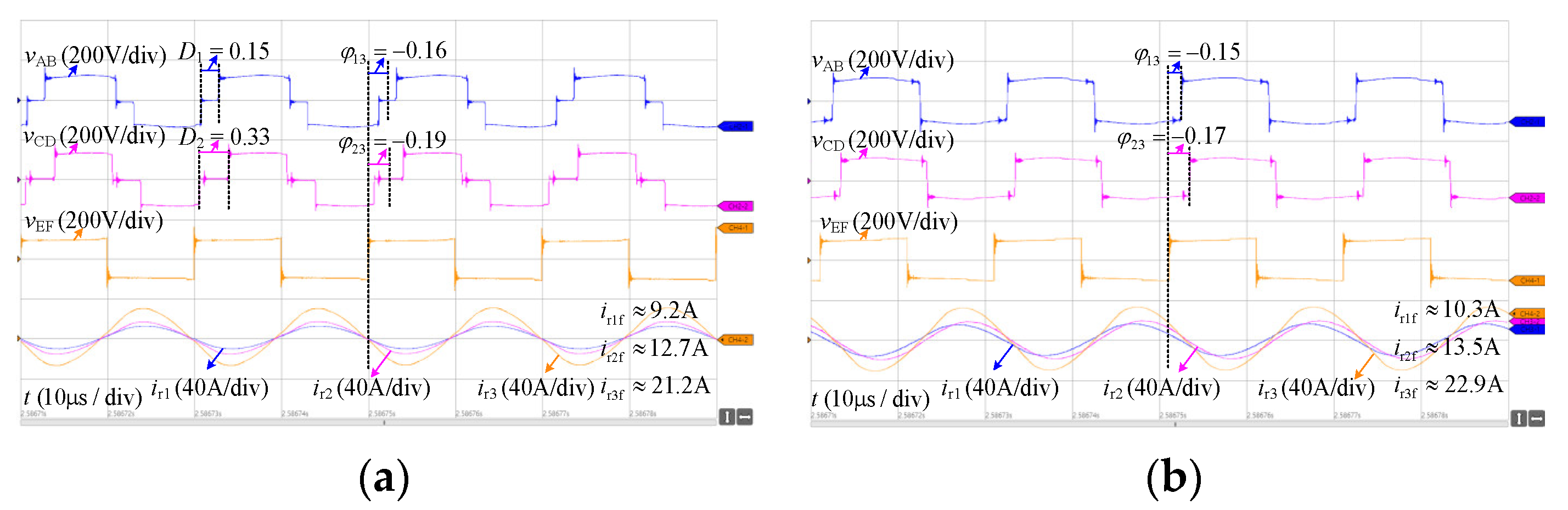
In the case of
k1 > 1, the voltage of port 1 and port 2 are 60 V and 140 V, and
k1 and
k2 are 1.67 and 0.71, accordingly. The transfer power of port 1 and port 2 is 500 W and 1 kW, respectively.
D1,
D2,
, and
calculated by the optimal conditions in (27) are 0, 0.33, 0.20, and 0.19, respectively. In this case, the magnitude of
vAB is always smaller than
vEF, thus the modulation of port 1 is also simplified to the SPS modulation to minimise the RMS value of
ir1. The corresponding experimental waveforms of the two modulations are shown in
Figure 11. It can be seen that
ir2 is in a phase of
vEF of the optimized modulation. The RMS value of
ir2 and
ir3 of the optimized modulation are smaller than those of the SPS modulation. Since the topologies of port 1 and port 2 are exactly the same, the experimental results of state 3 are similar to those of state 2. They are not shown here.
The experimental waveforms of state 4 of the optimal modulation are shown in
Figure 12. The input voltage of port 1 and port 2 is 60 V and 80 V, and
k1 and
k2 are 1.67 and 1.25, accordingly. Since
k1 and
k2 are both greater than 1 in this state, the RMS value of the transformer current is minimized when the RMS value of
vAB and
vCD is the maximum. Hence, the optimized modulation is simplified into SPS modulation.
The above experimental results show that the RMS value of the transformer current under the optimized modulation is effectively reduced compared with the SPS modulation in the entire power range. Hence, the power loss of the converter is reduced.
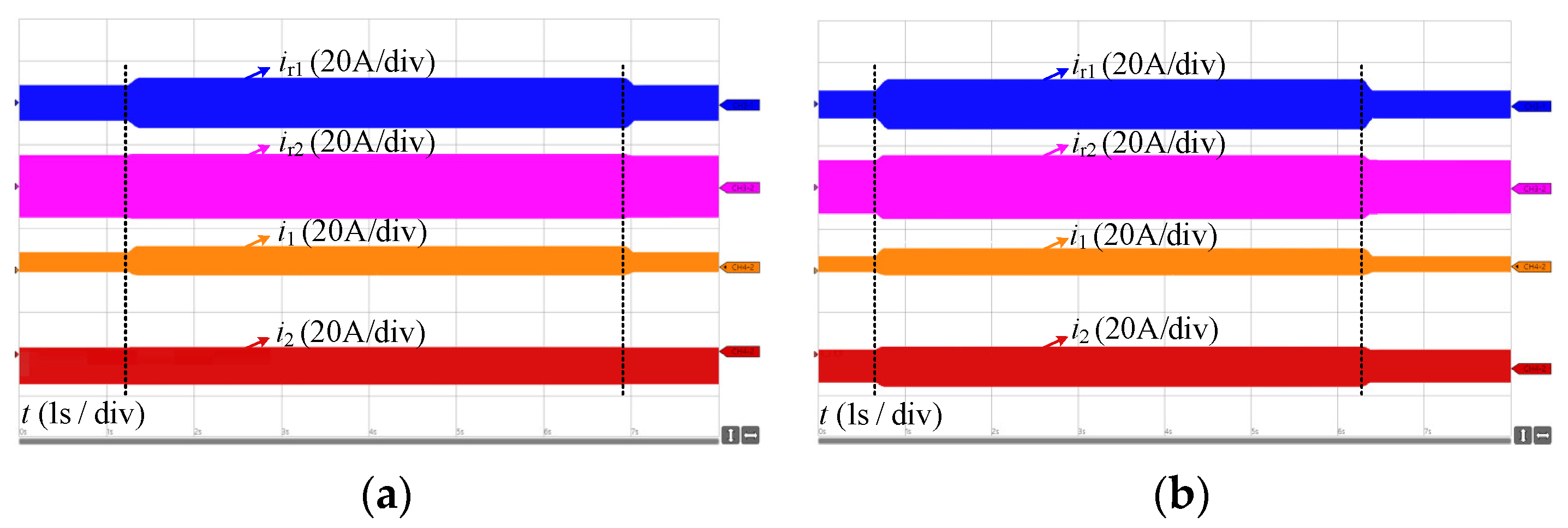
Then, the effectiveness of the power decoupling and the optimized modulation of both port 1 and port 2 operating at the backward mode are tested.
Figure 13a shows the experimental results when the desired
i2 remains constant while
i1 is suddenly stepped. From
Figure 13a, when
i1 is suddenly stepped, the actual
i2 remains constant. It means the proposed converter realizes the power decoupling in this case.
Figure 13b shows the experimental results of the conventional TAB converter under the same conditions. From
Figure 13b,
i2 varies when
i1 is stepped. Next, take state 1 as an example to test the optimized modulation. The steady-state waveforms are shown in
Figure 14. Both port 1 and port 2 operate at the minimum transformer current and the RMS value of the transformer current is effectively reduced compared with the SPS modulation.
Similarly, the dynamic waveforms of port 1 operate in the forward mode and port 2 operating in the backward mode are shown in
Figure 15. The corresponding steady-state waveforms under the optimized modulation are shown in
Figure 16. These experimental results verify the converter eliminates the power coupling between port 1 and port 2 and reduces the RMS value of the transformer current under the hybrid mode.
From the above experimental results, the proposed topology realizes the power decoupling, and the proposed modulation also significantly reduces the transformer current, in the entire power range and various operation modes.
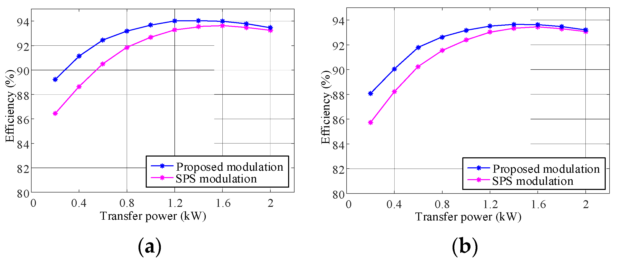
Finally, take both port 1 and port 2 operating at the forward mode as an example to test the efficiency of the proposed converter under the proposed modulation and SPS modulation. The efficiency is tested and compared in the different states. The efficiency curves in the state of
k1 < 1 and
k2 < 1 are shown in
Figure 17a. The efficiency curves in the state of
k1 > 1 and
k2 < 1 are shown in
Figure 17b. It can be seen that the efficiency is all over 88% in the different states. Compared with the SPS modulation, the efficiency of the optimized modulation is effectively increased in a wide range of the transfer power and the voltage gain.


