Article

Effect of Optical–Electrical–Thermal Coupling on the Performance of High-Concentration Multijunction Solar Cells

Guangdong Provincial Key Laboratory of Photovoltaic Technology, School of Physics, Sun Yat-sen University, Guangzhou 510006, China
*
Author to whom correspondence should be addressed.
Appl. Sci. 2022, 12(12), 5888; https://doi.org/10.3390/app12125888
Submission received: 23 May 2022 / Revised: 5 June 2022 / Accepted: 7 June 2022 / Published: 9 June 2022
(This article belongs to the Topic Optical and Optoelectronic Materials and Applications)

Abstract

:
In the process of high-concentration photovoltaic (HCPV) power generation, multijunction cells work in the conditions of high radiation and high current. Non-uniformity of focusing, the mismatch between the focusing spectrum caused by the dispersion effect and the spectrum of multijunction solar cell design and the increase in cell temperature are the key factors affecting the photoelectric performance of the multijunction solar cell. The coupling effect of three factors on the performance of multijunction solar cell intensifies its negative impact. Based on the previous research, the light intensity and spectral characteristics under Fresnel lens focusing are calculated through the optical model, and the optical–electrical–thermal coupling model under non-uniform illumination is established. The results show that obvious changes exist in the concentration spectrum distribution, energy and non-uniformity along different optical axis positions. These changes lead to serious current mismatch and transverse current in the multijunction solar cell placed near the focal plane which decreases the output power. The lost energy makes the cell temperature highest near the focal plane. In the condition of passive heat dissipation with 500 times geometric concentration ratio, the output power of the solar cell near the focal plane decreases by 35% and the temperature increases by 15%. Therefore, optimizing the placement position of the multijunction cell in the optical axis direction can alleviate the negative effects of optical–electrical–thermal coupling caused by focusing non-uniformity, spectral mismatch and rising cell temperature, and improve the output performance of the cell. This conclusion is verified by the experimental result.

1. Introduction

With the development of photovoltaic technology, many cell technologies such as crystalline silicon cells (c-Si), thin-film cells [1,2], multijunction cells and emerging PV technology [3,4,5,6] were born and play import roles. Compared with other technologies, multijunction solar cells are commonly used in concentrated photovoltaic (CPV) technology for its special advantages such as reducing cell area, high conversion efficiency and withstanding high temperature [7]. In order to enhance the spectral response, its development has changed from three junction, four junction to even more junctions [8,9]. The latest record of multijunction solar cell has reached 47.1% and the latest record of module efficiency is 38.9% [9,10,11]. Multijunction cells are usually composed of III-V compound semiconductors. GaAs-based compounds and InP-based compounds are commonly used.
During the processing of power generation, the photoelectric performance of the solar cell is affected by many factors such as non-uniformity of concentration [12,13], spectral response [14] and temperature [7,15,16,17,18,19], which may cause obvious losses of photoelectric conversion of solar cells. Hasan Baig et al. [12] summarized nine factors that mainly lead to the decline in power generation efficiency and concluded that the non-uniformity of illumination will bring a decline of 4% of the system efficiency. The increase in cell temperature decreases efficiency by 7% and the spectral response cause an efficiency loss of 2%. A. Cuevas et al. [20] established a circuit model to study the effect of the concentrating cell under non-uniform illumination and indicated that there is still lateral carrier flow which makes the open circuit voltage lower than that under uniform illumination. A. Mellolt et al. [21] further studied and explored the current flow law on the surface of multijunction cells in open circuit state under non-uniform illumination. Based on the simulation results, the paper proposed to increase the density of grid lines in the central area of the solar cells to reduce the decline in filling factor (FF) and conversion efficiency caused by non-uniformity of illumination. Bunthof et al. [22] explored the influence of spectral mismatch on the photoelectric performance of CPV cells. They artificially constructed a spectral non-uniform state by placing different filters at both ends of the cell surface and found that the greater the distance between the two regions, the lower the filling factor and open-circuit voltage. Kumar et al. [23] explored the effect of cell temperature and concluded that the accumulation of thermal energy raises the temperature of the solar cells which will lead to a reduction in the cell conversion efficiency in turn and mechanical failures on the long-term operation of the cell.
In the outdoor application of high-concentration photovoltaic (HCPV) cells, multijunction solar cells are usually placed at the design focal plane of Fresnel lens. However, not only the irradiance of illumination on the cell surface is non-uniform, but also the spectrum of concentrating illumination is non-uniform. Our team’s previous research found that the characteristics of focusing along the optical axis have a great impact on the photoelectric conversion efficiency and the output performance of III-V multijunction concentrating photovoltaic cells at the focal plane is not the best [24]. When testing the newly developed cells, Steiner et al. [25] also found that the output current decreased slightly in the focal plane of the Fresnel lens and the filling factor fluctuated significantly in different optical axis positions. Li Xin et al. [26] analyzed the influence of dispersion effect on the output characteristics of multijunction cells and proposed that the negative influence of dispersion effect would be relieved by reducing the cell size. Our research showed that irradiance and spectral non-uniformity on the focal plane lead to the loss of spectral mismatch and reduce the photoelectric conversion efficiency of multijunction cells [24]. Moreover, due to the coupling between electricity and heat, the decrease in photoelectric conversion efficiency causes the temperature of the cell to increase, which further reduces the output performance. The electrical–thermal coupling effect is particularly prominent in non-uniform illumination.
In the outdoor operating environment, the output performance of solar cells is different from those under IEC standard due to variable irradiance, temperature and other factors [27]. Especially, in the field of high-concentration photovoltaics, non-uniformity of irradiation, spectral mismatch and increase in temperature are hot issues and a lot of research already exists about their effects on cell efficiency alone as mentioned above. The novelty of this paper is to combine these factors and consider their coupled effect on solar cells. Optimizing the placement of the solar cell is proposed to improve the output performance according to the results of coupling effect. The reasons for the novelty of this paper are in real power generation, non-uniform concentration and the change in temperature often occur at the same time and affect each other, which causes further change in the output of solar cells. When the cell is placed at the design focal plane, the efficiency of the cell will reduce due to non-uniform concentration. The lost electrical energy converts into internal energy to raise the cell temperature, which further reduces the output performance. The performance of the cell is affected by the electrothermal coupling produced by the non-uniform concentration and is not equal to the value in the standard testing condition. In order to study the influence of optical–electrical–thermal coupling in the actual operation of the HCPV cells, we established an optical–electrical–thermal coupling model. The non-uniform irradiance characteristics under the concentration of the Fresnel lens are simulated and spectral distribution characteristics along the optical axis position will be calculated to explore their influence on the mismatch among sub cells. Based on ANSYS, this paper depicts the cell temperature variation along the optical axis and analyzes the coupling effect on the cell output performance. The outdoor measurement was carried out to verify the coupling effect.

2. Theoretical Model
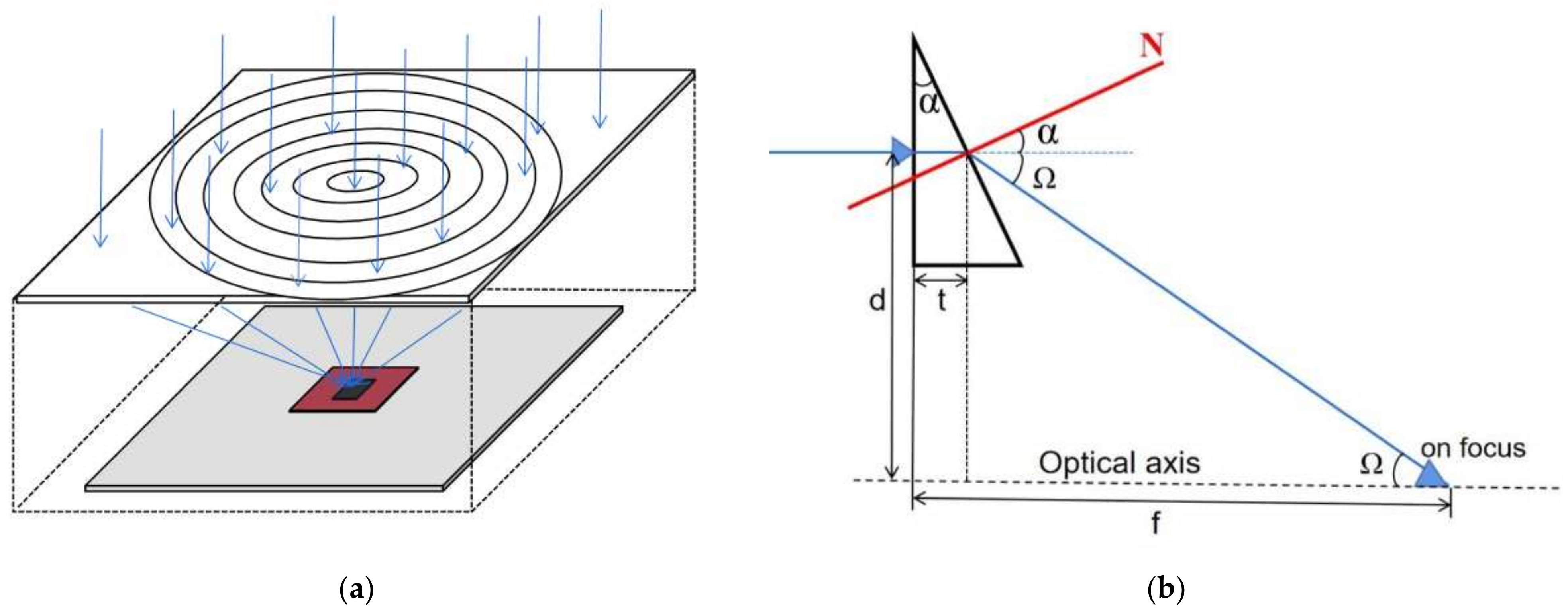
2.1. Optical Model

In the optical model without a homogenizer, the irradiance distributions of concentrated light were analyzed near the focal plane of the Fresnel lens. The physical structure of the concentrated photovoltaic cell is shown in Figure 1a. The irradiance is concentrated by a Fresnel lens, and the multijunction cell is placed directly under the Fresnel lens. The parameters of the Fresnel lens are as follows: material: PMMA (Poly (methyl methacrylate); aperture area: 15,125 mm2; thickness: 2 mm; focal distance estimated at 500 nm: 110 mm; and ring width: 0.5 mm. In this model, the position where the refracted light less than 500 nm intersects the optical axis will be at less than 110 mm. At the same time, due to the non-ideality of focusing, the intensity and spectral distribution of the concentrated illumination on the design focal plane are non-uniform.
The geometric relationships and the fundamental laws of refraction have been implemented in a programming environment to calculate the reflection position and the light power on the cell surface. The refracted light will go through three processes from the Fresnel lens to the surface of cells: (1) the incidence on the front surface of the lens; (2) the propagation through the lens; and (3) the exit from the rear surface of the lens. Figure 1b shows a 2D cross-section geometric relationships sketch of an incident light and its refracted light for a certain ring of the Fresnel lens. In the sketch, f represents the focal distance; d is the distance between the incident light and the lens center; t represents the distance between the refracted light and the front surface of the lens which equals half of the ring height if the light incidents from the middle of the ring; α is the incident angle and also equals angle of the slope of the facet; and Ω is the angle between the refracted light and the optical axis. According to the geometric relationships, Ω at 500 nm ( Ω 500 ) is estimated as follows:
Ω 500 = t a n 1 d f t
Once this angle is estimated, α at 500 nm ( α 500 ) is obtained by using the following relationship:
α 500 = t a n 1 s i n Ω 500 n 500 c o s Ω 500
where n 500 is the refractive index at 500 nm, its value being 1.49 [28], the Ω angle as a function of the wavelength can be estimated from the well-known Snell’s law as:
Ω λ = s i n 1 n λ · s i n   α 500 α 500
Based on the expressions above, the geometry slope of the refracted light functions as the wavelength and can be approximated. Ray tracing can be then performed for each ray height and wavelength. According to the spectral response of the triple junction cell, the spectral range is 300–1700 nm. The calculation takes a wavelength every 20 nm in this spectral range. The energy of this wavelength is obtained by integrating the wavelength in the positive and negative 10 nm range according to the solar power spectral density curve. A parameter (optical efficiency) is introduced here and it is defined as follows [29]:
μ = G I   ,
where G represents the irradiance actually irradiated on the cell surface; and I represents the incident irradiance with the area of Fresnel lens. The incident spectral irradiance inputted in the optical model is AM1.5D and the DNI is taken as a constant value of 1000 W/m2.

2.2. Optical–Electrical–Thermal Model of Non-Uniform Concentration

Under high concentration, the model is equipped with the triple-junction solar cells, type 3C44C produced by AZUR SPACE Solar Power GmbH [30]. The solar cell consists of GaInP/GaInAs/Ge. All sub cells are connected by tunnel diodes. The sub cells are simulated with the two-diode model which uses two diodes connected in parallel with a current source. According to the equivalent circuit, the current–voltage equation of three junctions is:
I = I Li I oi 1 exp qV i kT 1 I oi 2 exp qV i 2 kT 1 ,
where I Li (i = 1, 2, 3) represents the photogenerated current of the upper, middle and lower diodes. I oi 1 ,   I oi 2 (i = 1, 2, 3) are the reverse saturation currents of the upper, middle and lower layer diodes, respectively. The expression of the variation with temperature is as follows [31]:
I oi 1 T = A · k oi 1 · T 3 exp E gi T k B T ,
I oi 2 T = A · k oi 2 · T 5 2 exp E gi T 2 k B T ,
E gi T = E gi 0 α T 2 / T + β ,
where A is the area of the triple-junction cell; k oi 1 and k oi 2 are constants related to the cell material and can be calculated by fitting Equation (5), where the data are from irradiance-VOC measurements [32]; E gi T indicates the band gap width at temperature T; α and β are material-dependent constants; and k B is the Boltzmann constant.
Considering that the illumination from the Fresnel lens is non-uniform, the photoelectric conversion of solar cells is calculated by circuit network model [30,33,34,35]. As shown in Figure 2a,b, the multijunction solar cell is divided into several triple junction cells. Each sub cell is simulated by an electrical circuit based on the two-diode model. These two diodes represent the losses by recombination in the neutral and in the depletion region of the p–n junction. Because it is a 3D model, all of them have the lateral series resistance including both transverse and longitudinal resistance (R1x-R6x, R1y-R6y). Taking the GaInP sub cell as an example, the emission layer and the window layer are regarded as a whole and their lateral resistance in x, y direction is R1x, R1y. Similarly, the base layer and the back surface field are also regarded as a whole and their resistance is R2x, R2y, respectively. The sub cells are connected in tunnel diodes which in this model are fixed value resistors (Rsh1-Rsh3). R c represents metal-semiconductor contact resistor and Rf is the resistance of the grid finger. Since it is difficult to directly measure various resistance values of the triple-junction solar cells and the basic production process is almost similar, the simulation used the resistance data values in the literature [32]. It is worth noting that when the grid is divided according to the grid lines of the cell, there are two situations: One is the area that is not blocked by the metal grid line where the illumination can reach the cell surface to produce photoelectric effect. This is simulated by one current source and two diodes. The other is the area that is blocked by the metal grid line where the concentration cannot reach on the cell surface. In this case, only two diodes exist and the current source equals zero.
The equivalent circuit network model is calculated by NGSPICE. The input parameters include the series resistance Rs, the reverse saturation current of three sub cells I 0 i 1 and I 0 i 2 and the photogenerated current source I L i . The reverse saturation current can be obtained by fitting the relationship curve between the open-circuit voltage and light intensity. The series resistance of triple-junction cell can be unified with one resistance Rs determined according to the light and dark characteristic curve. As the short-circuit current of each junction cannot be measured separately, in this paper the photogenerated current is obtained indirectly through the external quantum efficiency (EQE) of the three sub cells [29]. The external quantum efficiency is defined as the ratio of the number of photogenerated carriers that contribute to the short-circuit current generated by illumination to the number of photons incident on the surface of the cell.
EQE λ = I L λ q φ λ ,  
It can be seen from Equation (8) that with the increase in temperature, the band gap of each sub cell decreases, which increases the absorbed wavelength range and changes the EQE at different temperatures. Here, we get the triple-junction cell EQE characteristic curve by measuring it at 25 °C. The EQE at other temperatures can be calculated by the linear interpolation method mentioned in the literature [29]. According to the optical model, the irradiance distribution incident on the battery surface can be calculated, which is the function of position of the cell surface x , y . If the density of the irradiance power on the cell is G λ , it can be expressed as follows:
G λ = f x , y                     ( x 1 < x < x 1 + Δ x , y 1 < y < y 1 + Δ y ) ,
Photon energy is calculated by h c / λ (where c is the speed of light and h is the Planck constant). The photogenerated current of a certain wavelength range [ λ 1 , λ 2 ] at a given temperature can be expressed as follows:
I L = λ 1 λ 2 q E Q E λ G λ λ h c d λ

2.3. Heat Transfer Model

Non-uniform illumination not only affects photoelectric performance but also affects the temperature distribution of the module receiver. ANSYS is used to simulate finite element coupled multiple physics fields and calculate the temperature distribution of the receiver at different positions along the optical axis. The receiver consists of a multijunction solar cell, DBC (Direct Bonded Copper) and heat sink. DBC is used to maintain the electrical insulation between the cell and the base plate has good performance on thermal conductivity. Figure 3 shows the heat dissipation diagram of the receiver.
The receiver is divided into five layers according to the types of materials. The top layer is the triple-junction solar cell. As the main component of the cell is Ge, the cell material can be set as Ge in the calculation of heat dissipation model. The DBC layer is divided into three parts: the upper layer and lower layer are copper and the middle layer is ceramic. The upper copper layer is also used as an electrode of the cell, and the ceramic layer is used for electrical insulation. The bottom layer is aluminum for heat dissipation [36]. Table 1 lists the material and thickness of each layer of the receiver.
In the photovoltaic module, the sunlight converges to the cell surface through the lens to join in photoelectric conversion. Part of the remaining light energy is reflected by the cell surface and part is converted into internal energy of the cell [37]. The illumination energy converted into the internal energy is used as the boundary heat source [38] flowing into the cell. Because the cell efficiency is related to temperature, the boundary heat source can be considered as a function of temperature. In passive cooling environment, for the cell layers, the exposed surface of the DBC layer and heat dissipation aluminum layer, the boundary equations can be expressed as follows:
k i T i y = Q 1 i + Q 2 i ,
where k i and T i are thermal conductivity and temperature of each layer, Q 1 i refers to the radiation heat transfer with surrounding environment and Q 2 i represents the convection heat transfer with air [39]. They can be expressed as the following equations:
Q 1 i = ε i · A i · T i 4 T s 4 ,  
Q 2 i = h conv i T i T amb ,
where ε i and A i are the emissivity and heat exchange area of each layer; h conv i is the convective heat transfer coefficient of each layer; and T s is the sky temperature. For two adjacent materials (i, j), the heat is transferred in the way of heat conduction. The boundary condition of them can be expressed as follows:
k i T i y = k j T j y ,

3. Calculation Results and Analysis

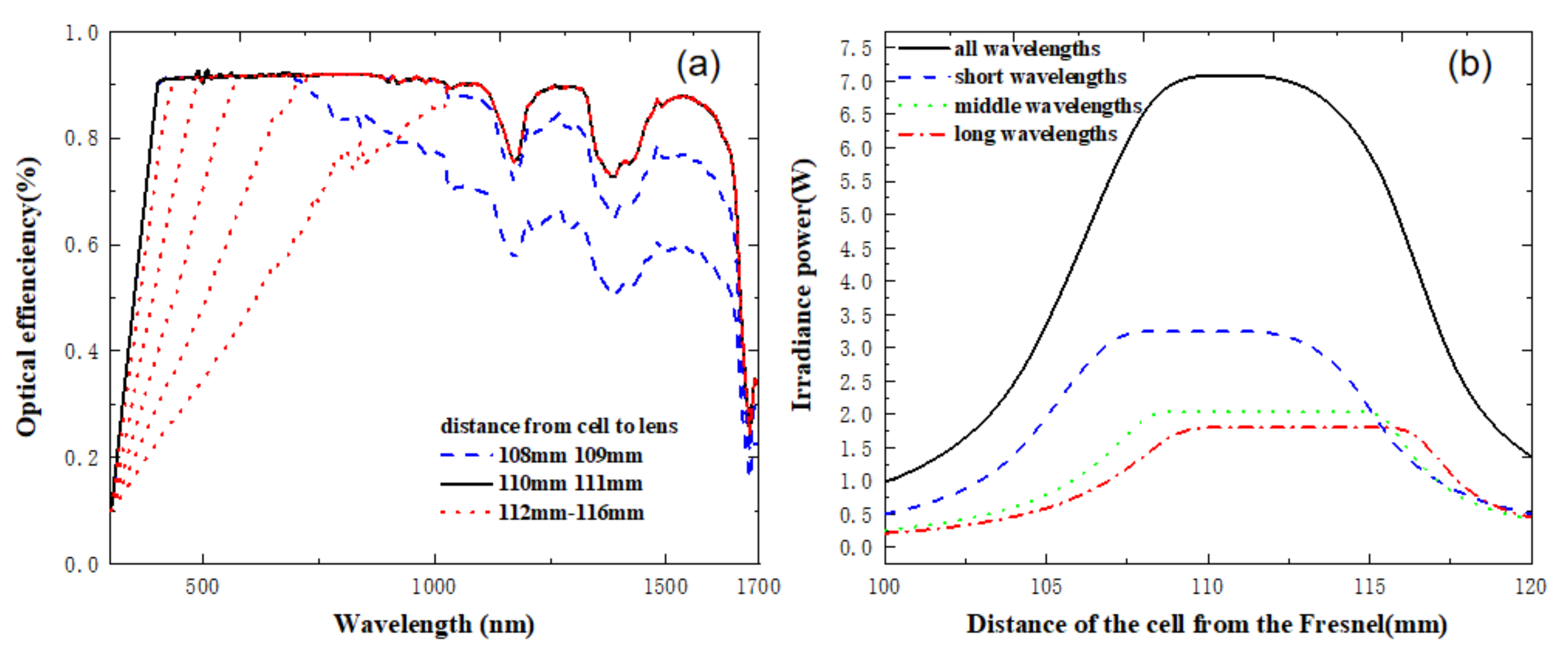
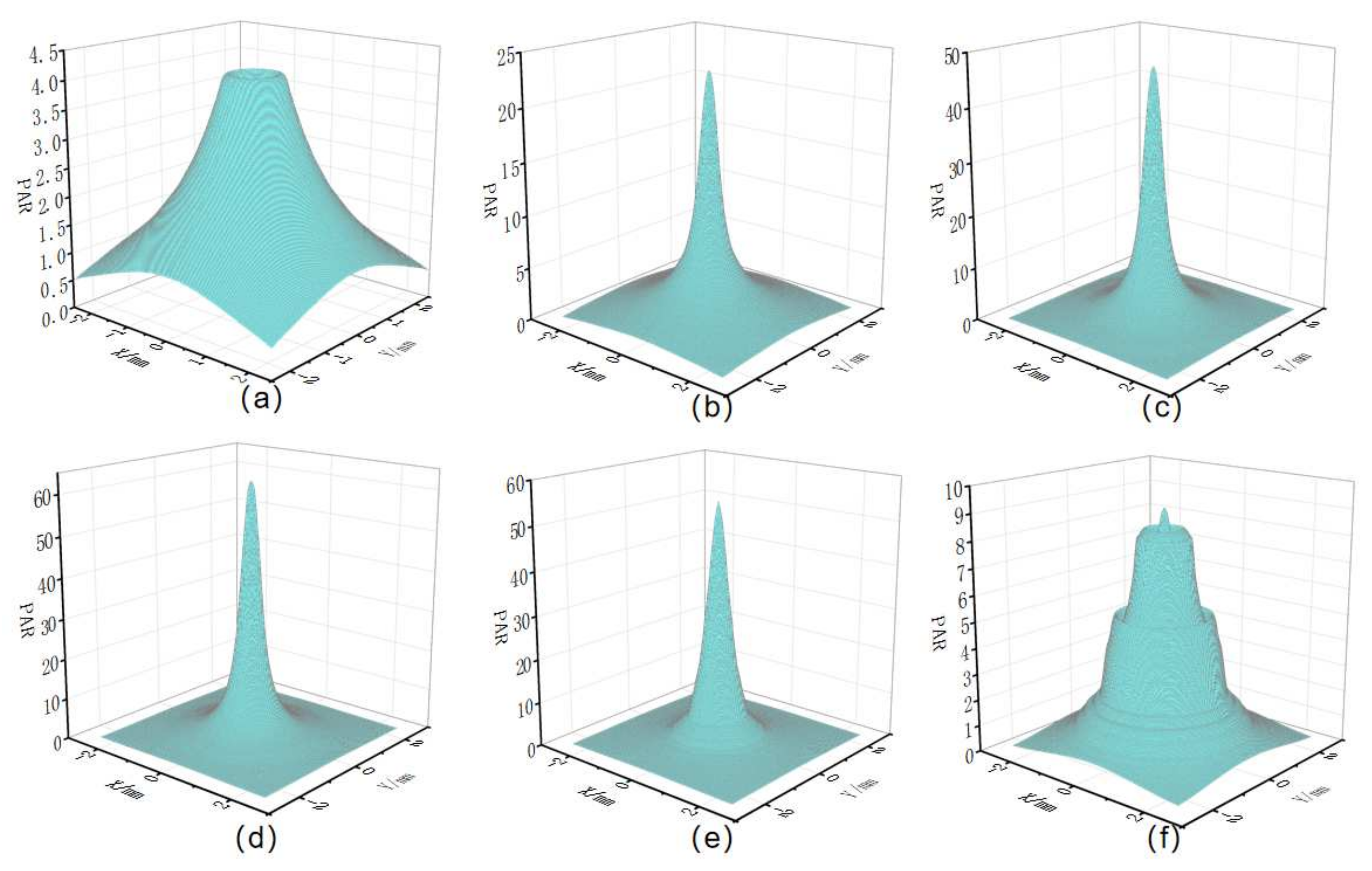
3.1. Concentrated Light Intensity and Spectral Analysis along the Optical Axis

The optical efficiency calculations in the optical model are shown in Figure 4a for several distances of the receiver from the Fresnel lens position (Z). The on-focus position is at Z = 110 mm. As can be seen from that, the optical efficiency of the Fresnel lens is related to the distance from the cell to the lens. For Z = 110 and 111 mm, the optical efficiency of the full-wave band is maximum. The optical efficiency of the short-wave band decreases at Z = 112 mm. With the distance from the cell to the lens being further, the optical efficiency of 500 nm decreases to 34.5% at 116 mm. The optical efficiency of long wavelength decreases at Z = 109 mm and the optical efficiency of 1500 nm decreases to 76.4%. When the distance is 108 mm, the optical efficiency of the medium-wave band begins to decrease and the long-wave band continues to decrease which the optical efficiency of 1500 nm has decreased to 59%.
The optical efficiency of the lens at different optical axis positions is different, indicating that it is affected by the dispersion effect. When the distance from the lens to the cell is less than the focal distance, long wavelength efficiency decreases because the cell surface cannot cover all illuminations and part of long-band sunlight is lost. For Z > 100 mm, the short band optical efficiency decreases, and part of the short band light cannot be concentrated on the cell surface. When the cell is placed at the focal plane, there is no energy loss, but the short-wave spot is smaller and more concentrated in the center of the cell whose distribution is seriously non-uniform. It can be seen that due to the dispersion effect, the energy proportion of the three bands irradiated on the cell does not change synchronously, and there is spectral mismatch at different optical axis positions (including on the focal plane). The spectral distribution deviates from the solar spectrum, which is bound to make an adverse impact on the performance of the cell. Figure 4b shows the change in the irradiance power calculated with the position of the optical axis, reflecting the changes in the short, medium and long bands, respectively. It can be seen that the changes in the irradiance power of the medium band and long band are basically the same. The maximum value position is between 110 and 116 mm and the position of the maximum value of the short band radiation power is between 108 and 111 mm which is consistent with the change tendency of the optical efficiency reflected in Figure 4a. Because the radiation power of the short-wave band accounts for about half of the total radiation power, the total change in the radiation power is mainly affected by the short-wave band.
In addition to the dispersion effect, the spot focused by the Fresnel lens also has obvious Gaussian distribution. This kind of non-uniformity also has an important impact on the output characteristics of multijunction solar cells [21]. Therefore, this paper explores the change in the spot non-uniformity along the optical axis. Figure 5 shows the spot diagram at typical positions along the optical axis (Z = 108 mm, 109 mm, 110 mm, 111 mm, 112 mm and 114 mm). Concentration ratio is defined as the ratio of the actual irradiance on the cell surface to the standard irradiance (1000 W/m2) and the peak to average ratio (PAR) is defined as the ratio of the highest irradiance on the cell surface to the average irradiance on the surface, which is used to quantify the non-uniformity of the spot. When the cell is located at Z = 108 mm, the central focusing ratio is about 283 and the PAR is 4. When the cell is placed near the focal plane (for a range of Z values between 110 and 112 mm), the non-uniformity increases rapidly and the PAR increases to 47.2, 62.7 and 55.0. When the cell is far away from the focal plane (at Z = 114 mm), the non-uniformity begins to improve and the par falls back to 9.1. The maximum PAR of the short, medium and long bands and their positions on the optical axis are shown in Table 2. The maximum PAR of the short, medium and long bands is at Z = 110.5 mm, 111.4 mm and 112.3 mm. The maximum PAR of the full-wave band is at Z = 111.8 mm, which is the result of the synthesis of the three bands. The non-uniformity of focusing is strong near the focal plane. On the contrary, there is a better uniform spot away from the focal plane. The output characteristics of the triple-junction cell placed near the focal plane will be negatively affected by the non-uniformity. Improving the distance from the cells to the lens can improve the output performance.

3.2. Analysis of the Cell Temperature along the Optical Axis

When the parameters of the Fresnel lens and cell are determined, the illumination along the optical axis is determined. In addition, the power generation performance of photovoltaic cells is affected by temperature, which is affected by the cooperation of the optic–electric–thermal. In order to determine the parameters of photoelectric conversion, it is necessary to calculate the temperature of the cell in the steady state. Through the optical–electrical–thermal coupling model, the temperature distribution of the receiver and the thermal response of the cell at different positions are calculated. Figure 6 shows the surface temperature distribution of the receiver at 108 mm, 109 mm, 110 mm, 111 mm, 112 mm and 114 mm when the ambient temperature is 25 °C and the heat transfer coefficient is 10   W / m 2 K . Figure 6a shows that the surface temperature of the cell reaches 49.8 °C at Z = 108 mm and the minimum temperature is 39.9 °C on the edge of the receiver. Figure 6b shows that the surface temperature of the cell at 109 mm is 53.4 °C and the edge temperature of the receiver is 42.1 °C. In Figure 6c, the cell is at the design focal plane of the lens where the surface temperature rises to 55 °C and the temperature at the edge of the receiver is 43.1 °C. In Figure 6d, the surface temperature of the battery continues to rise to 55.5 °C at Z = 111 mm.
In Figure 6e, the cell is located at 112 mm, the temperature of the cell surface is a maximum of 57.4 °C and the temperature of the receiver edge is 44.4 °C. In Figure 6f, the cell temperature decreases and the surface temperature decreases to 51.4 °C. The minimum temperature of the receiver decreases to 40.9 °C. From the temperature change trend of the cell, it can be noticed that when Z < 112 mm, the temperature of the cell gradually increases in the direction away from the lens. The temperature of the cell is the highest at 112 mm. With the distance is further, the temperature of the cell gradually decreases. It can be seen that the temperature change in the cell surface is basically consistent with the change in radiation power because the surface temperature distribution of the receiver is related to the heat dissipation. The illumination non-uniformity near the focal position is the most serious thus causing photoelectric efficiency to decrease. The value of temperature is the highest for Z = 112 mm. In addition, the temperature difference between the cell and the edge of the receiver at 116 mm is 7.5 °C while the temperature difference at 112 mm is 13 °C. The higher the heat dissipation, the greater the temperature gradient inside the cell, resulting in a greater temperature difference between the cell and the edge of the receiver.

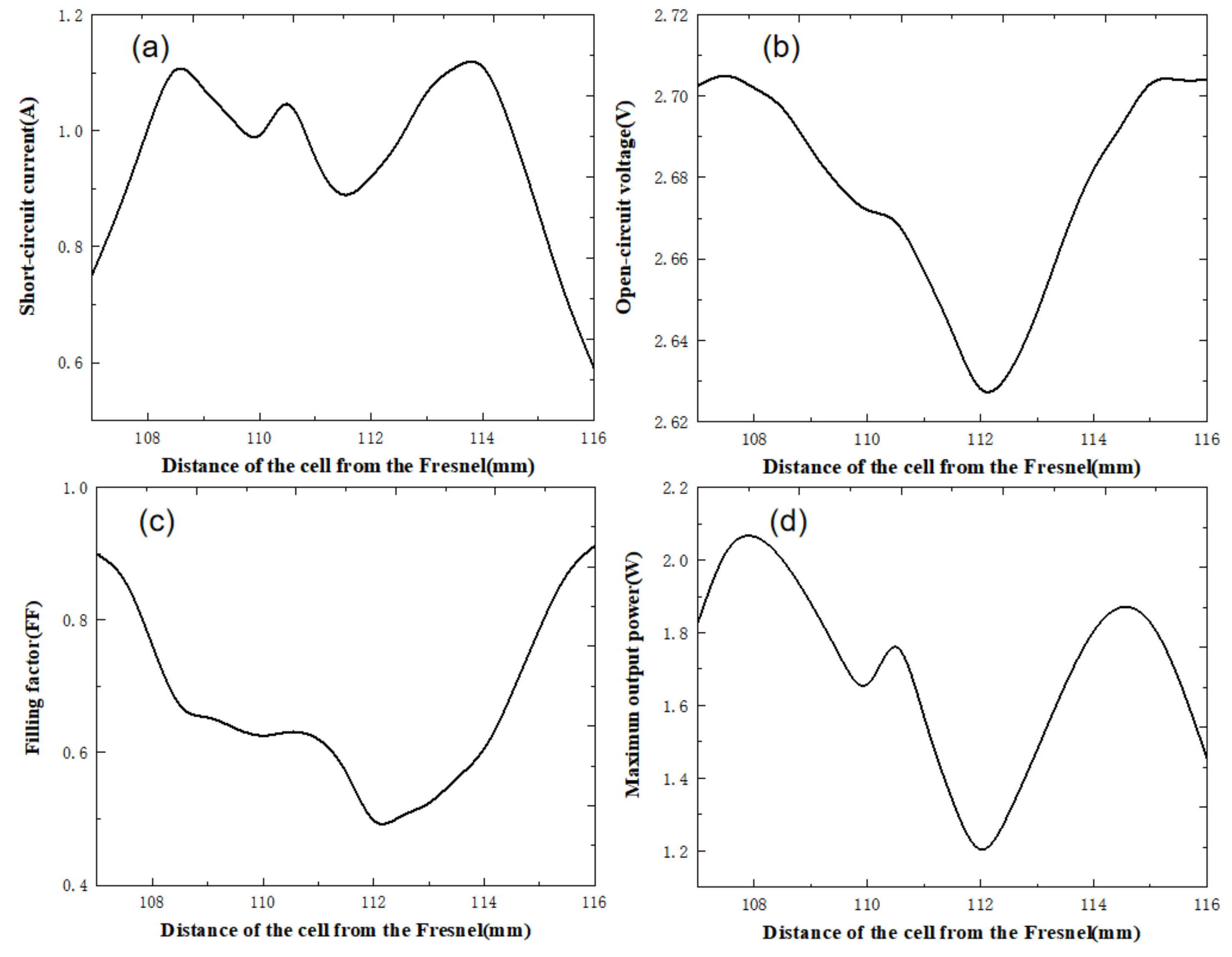
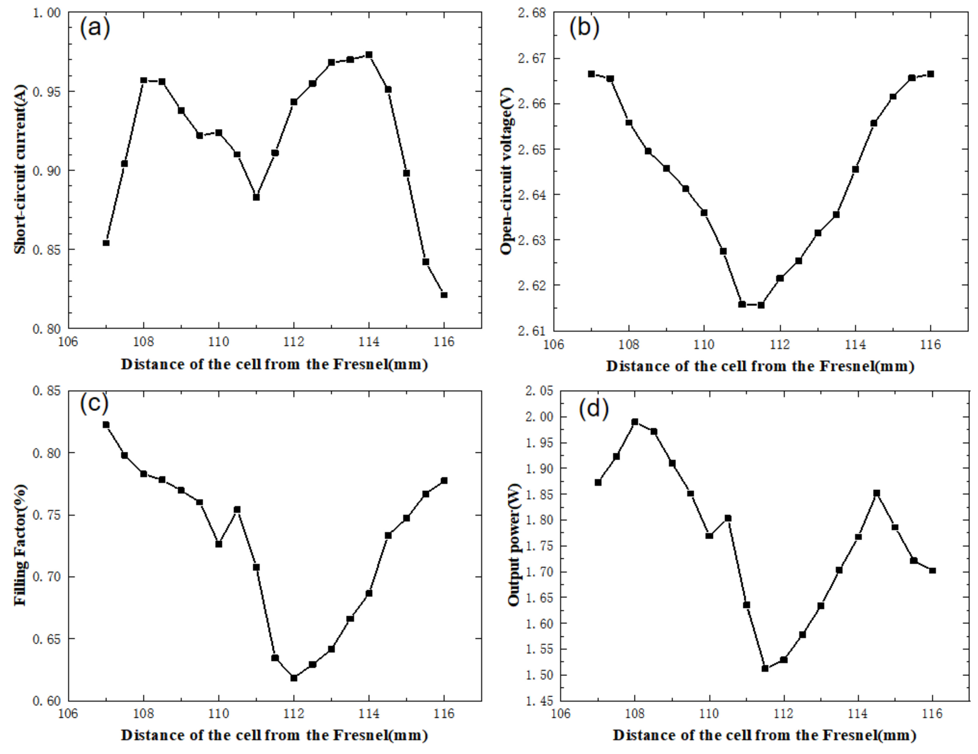
3.3. Analysis of the Optical–Electrical–Thermal Coupling Effect of Output Characteristics

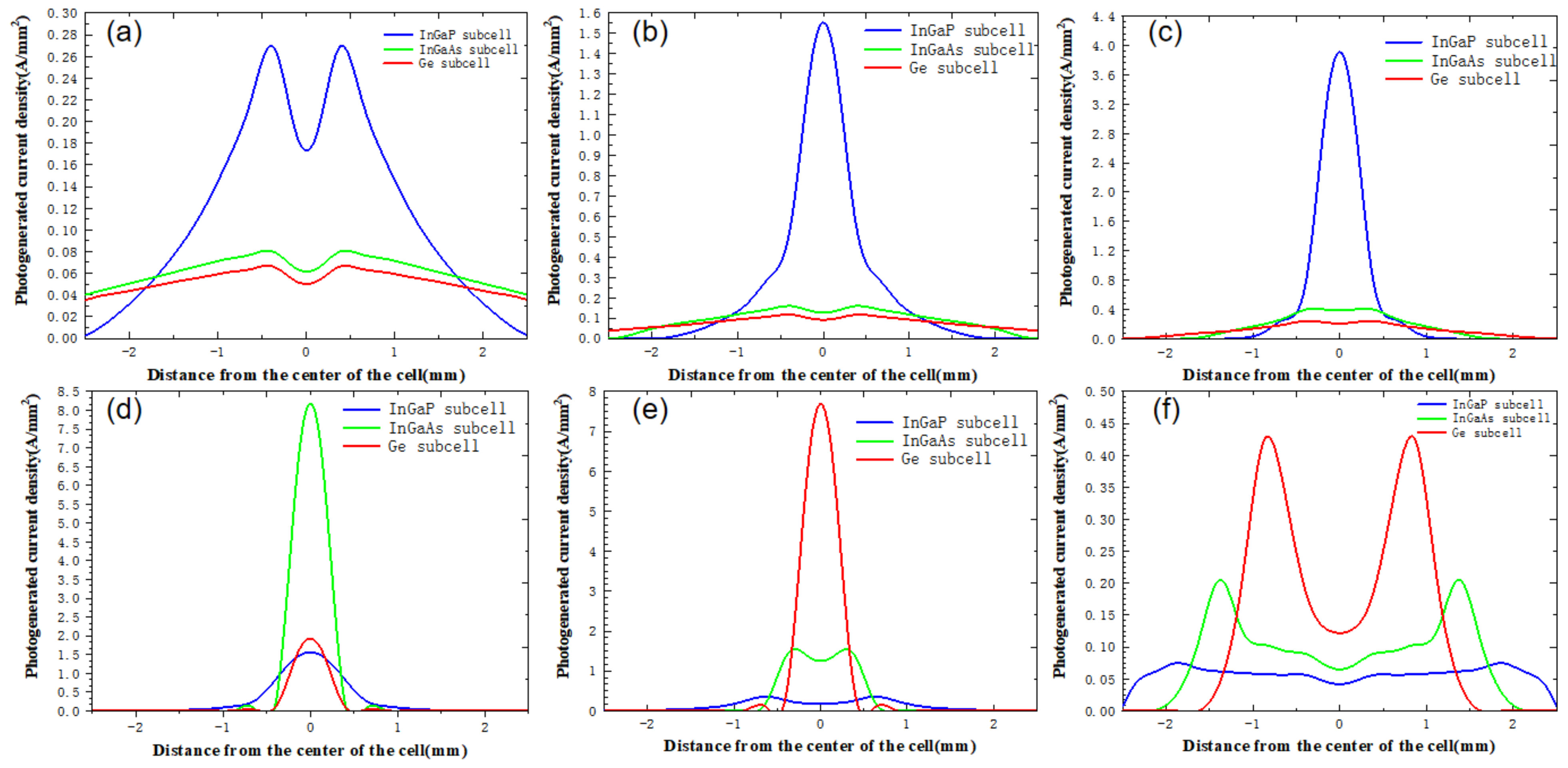
3.3.1. Short-Circuit Current

The change in the short-circuit current of the triple-junction cell along the optical axis is shown in Figure 7a. It can be seen that although the radiation power near the focal plane is the strongest, the short-circuit current of the cell is minimum near the focal plane and the maximum value on both sides (Z = 108.5 mm, 114.0 mm) is about 24% higher than it, which is related to the current mismatch between sub cells caused by non-uniform irradiance and dispersion effect.
Figure 8 shows the variation in photogenerated current density of InGaP, InGaAs and Ge in the direction of cell surface and 0 mm is the center position of the cell. Figure 8a–f show the cases where the cell is placed at 108 mm, 109 mm, 110 mm, 111 mm, 112 mm and 114 mm, respectively. It can be seen that the photogenerated current is approximately Gaussian distributed and there is an obvious current mismatch between the sub cells especially in the central area.
Comparing Z = 110 mm (on-focus position) with Z = 108 mm, when the cell is at the focal plane, the photogenerated current density of the InGaP sub cell is 3.427 A / mm 2 at 0 mm (center of the cell). InGaAs sub cell is 0.396 A / m m 2 and the photogenerated current density of the Ge sub cell is 0.219 A / m m 2 . The photogenerated current density of the InGaP sub cell is significantly higher than that of the InGaAs and Ge sub cells and is about 16 times higher than that of Ge. When the cell is located at 108 mm, the current density of the InGaP sub cell is slightly higher than that of the InGaAs and Ge sub cells, which is about 4 times higher than the Ge sub cell. The current mismatch is greatly improved. It can also be seen that at the focal plane, the central photogenerated current density of InGaP is 265 times that of 1 mm from the cell center. Meanwhile, when Z = 108 mm, the central photogenerated current density of the upper sub cell at 0 mm is 1.5 times than that at 1 mm from the cell center. It can be seen that the lateral current caused by the non-uniformity of the focusing is also greatly improved. For a range of Z values between 108 to 110 mm, the photogenerated current of InGaP sub cell in the central area is greater than that of the InGaAs and Ge sub cell because short wavelengths basically have maximum radiation power while the radiation power of medium and long bands do not reach maximum value. When the cell is placed at the on-focus position, the PAR of short wavelengths is close to the maximum and the photogenerated current of InGaP sub cell in the central area also reaches maximum. For the InGaAs and Ge sub cells, the position of maximum PAR values are 111.4 mm and 112.3 mm so they have the maximum photogenerated current at relevant positions.
Under non-uniform illumination, the overall short-circuit current of the multijunction solar cell is affected by vertical current mismatch between the sub cells. Generally, the overall output current will be limited by the minimum current of the sub cells [40,41]. In order to explore the influence of vertical current mismatch, we calculated the short-circuit current of each sub cells [42]. Figure 9a shows the short-circuit current of the InGaP, InGaAs and Ge sub cells. The minimum values occur at 110 mm, 111 mm and 112 mm, respectively, which is affected by the non-uniformity of light spots of short, medium and long wavelengths. The optical axis position of the minimum short-circuit current is basically consistent with the position of the maximum PAR (Table 2). Moreover, current mismatch exists between sub cells in the range of Z values between 107 to 116 mm. For Z < 108 mm, the short-circuit current of the InGaP sub cell was slightly larger than that of InGaAs and Ge because the spot diameters of three bands are larger than the size of the cell while the spot of short wavelengths is relatively more concentrated. From 108 mm to 114 mm, the minimum value of the short-circuit current of each sub cell is taken and compared with the short-circuit current of the triple-junction solar cell (Figure 9b). The curve of the minimum value of the short-circuit current of the sub cell basically coincides with the curve of the triple-junction solar cells. However, when the cell was between 108 and 114 mm, the short-circuit current of the triple-junction cell is less than the minimum value of the short-circuit current of each sub cell, indicating that serious current mismatch exists near the focal position.

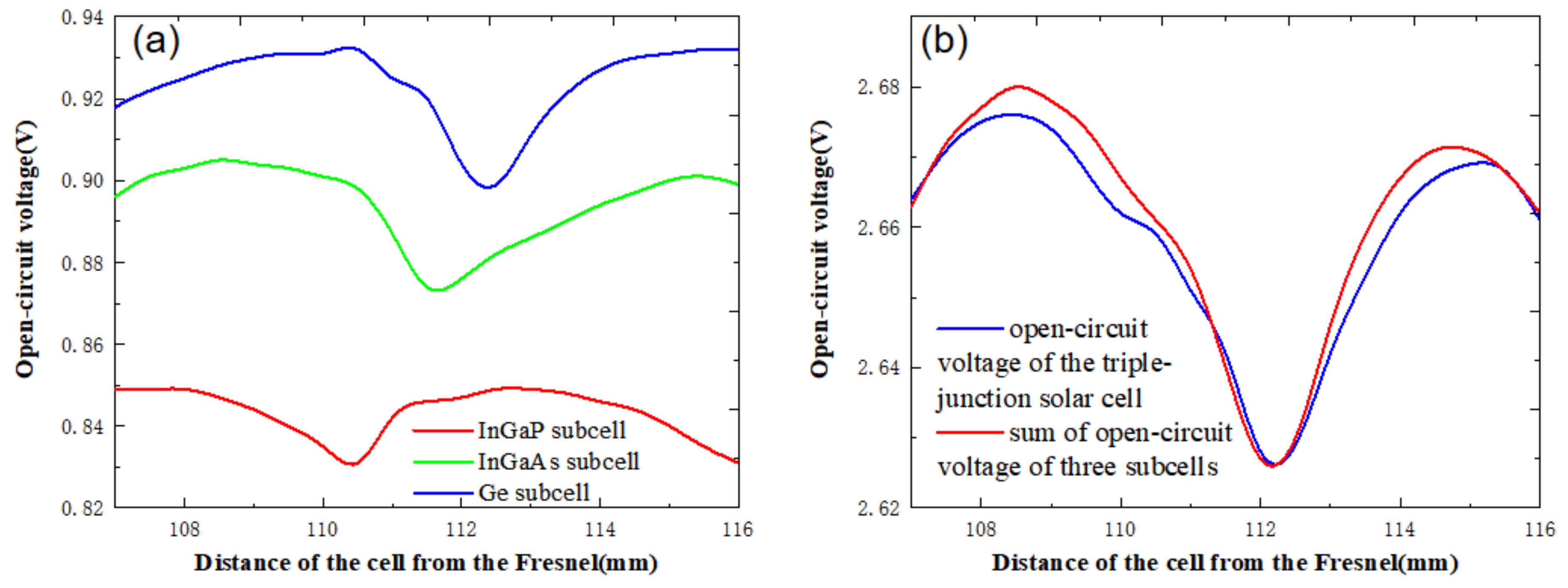
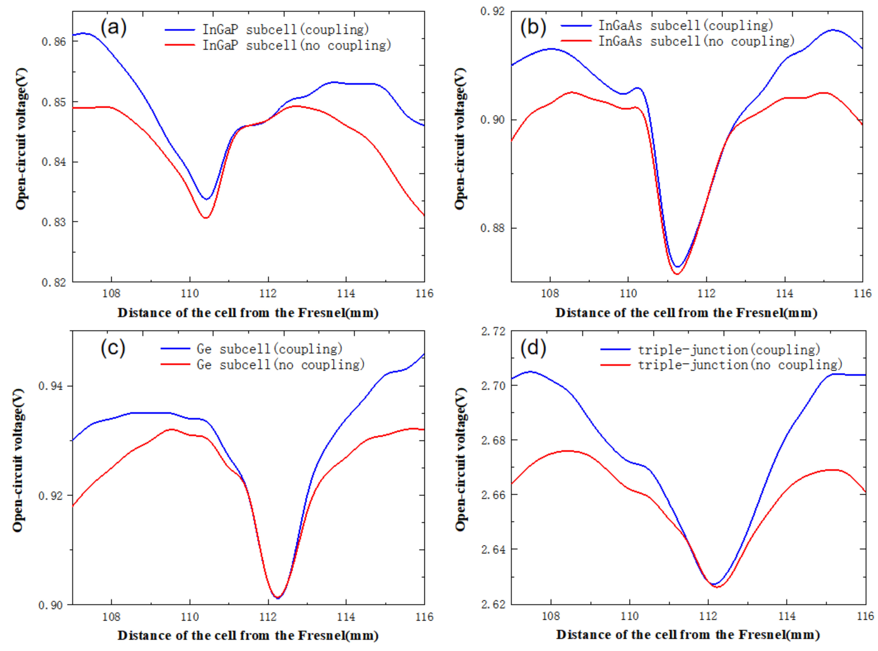
3.3.2. Open-Circuit Voltage

The change in the open-circuit voltage along the optical axis is shown in Figure 7b. It can be seen that a minimum of the open-circuit voltage near the focal plane also exists, and the maximum on both sides (Z = 108 mm, 114.5 mm) is about 3% higher than it, which is related to the optical–electrical–thermal coupling effect caused by the non-uniform focusing.
Figure 10a shows the change in the open-circuit voltage of the InGaP, InGaAs and Ge sub cells along the optical axis without considering the temperature. It can be seen that the open-circuit voltages of the InGaP, InGaAs and Ge sub cells of the triple-junction cell reach minimum at the position of Z = 110 mm, 111 mm and 112 mm, respectively. The non-uniformity of the focusing and the mismatch between the sub cells will decrease the open-circuit voltage. Due to the non-uniformity of illumination, the carrier concentration is non-uniform and a potential difference on the surface of the emission region exists, resulting in transverse current on the cell surface [43]. It can be seen from the diode model of the solar cell that the greater the transverse potential difference on the cell surface, the smaller the open-circuit voltage of the cell. The open-circuit voltage changes exponentially with the radiation power. Therefore, when the concentration heterogeneity increases, the carrier concentration gradient on the surface of the cell increases thus increasing the surface potential difference. Figure 10b compares the sum of the open-circuit voltage of the InGaP, InGaAs and Ge sub cells with the open-circuit voltage of the triple-junction solar cell. The sum of the open-circuit voltage of the sub cells basically coincides with the curve of the triple-junction cell, indicating that the open-circuit voltage of the triple-junction solar cell is mainly the result of the non-uniform irradiance.
In order to analyze the influence of optic–electric–thermal coupling on the open-circuit voltage specifically, a photoelectric conversion simulation without considering coupled effect is set in this paper in which the temperature of the cell along the optical axis is set as a fixed value for calculation. Figure 11 shows the comparison of the open-circuit voltage characteristics of each sub cell and the whole cell with coupling and no coupling. When there is no coupling effect, the maximum open-circuit voltage of triple-junction cells is 2.675 v at Z = 108 mm, which is 0.047 v greater than the minimum value of 2.628 v at Z = 112 mm. When considering the optical–electrical–thermal coupling, the maximum voltage is 2.702 v at Z = 108 mm, which is 3% higher than the minimum. Compared with no coupling, the difference between the maximum and minimum of open-circuit voltage increases by 57.4%. The change in the open-circuit voltage along the optical axis cannot be ignored due to the optical–electrical–thermal coupling caused by the non-uniform irradiance. The minimum of open-circuit voltage near the focal plane is caused by the strongest optical non-uniformity and the optical–electrical–thermal coupling exacerbates the decrease in open-circuit voltage. On the contrary, at the position slightly away from the focal plane, due to the great improvement of the non-uniformity, the photoelectric conversion efficiency is improved and the boundary heat source is reduced. Under the same conditions of heat dissipation, the temperature at the position slightly away from the focal plane is reduced, which further improves the output performance of the cell and the optical–electrical–thermal coupling further increases the open-circuit voltage.

3.3.3. Output Power

Besides the short-circuit current and open-circuit voltage, the filling factor and maximum power also change with the installation position of the cell (Figure 7c,d). When Z = 112 mm, the illumination non-uniformity is the strongest and the filling factor is the lowest, which is about 50%. At the position away from the focal plane, the filling factor is close to 90%. The filling factor is mainly closely related to the non-uniformity of concentration. In the case of non-uniform illumination, the current generated in the highly illuminated central area of the cell flows to the darker edge area through the grid line where the transverse current is generated and the effective series resistance is increased [23,44]. The conversion efficiency is lower than that in the case of current matching and the filling factor also decreases. The filling factor has an obvious negative correlation with PAR. Optimizing the distance can improve the non-uniformity of the illumination so as to improve the filling factor. Figure 7d shows the variation in the maximum output power of the triple-junction cell along the optical axis. The minimum output power at the focal plane is 1.21 w, while the maximum output power at both sides of the focal plane (Z = 108 mm, 114.5 mm) is 2.06 wand 1.85 w. When the cell is placed at the focal plane, the maximum output power decreases by 35%. The main reason is the decrease in the short-circuit current, open-circuit voltage and filling factor caused by the non-uniform illumination as well as the negative impact of comprehensive optical–electrical–thermal coupling. Compared with the short-circuit current and open-circuit voltage, the filling factor fluctuates more significantly. The filling factors at 108 mm, 110 mm and 114.5 mm in the optical axis direction are 76%, 62.6% and 68.8%, respectively. The optical–electrical–thermal coupling intensifies the negative effect of the non-uniformity near the focal plane, causing the cell temperature to increase by 15%, the open-circuit voltage to decrease from 2.7 v to 2.63 v and the maximum output power to decrease further by 1.2%. It can be seen that the coupling effects of the non-uniformity of the focusing, the spectral mismatch between the focusing spectrum and the multijunction cell design and the increase in cell temperature are the key reasons for the decline in the output power of the multijunction cell near the focal plane.

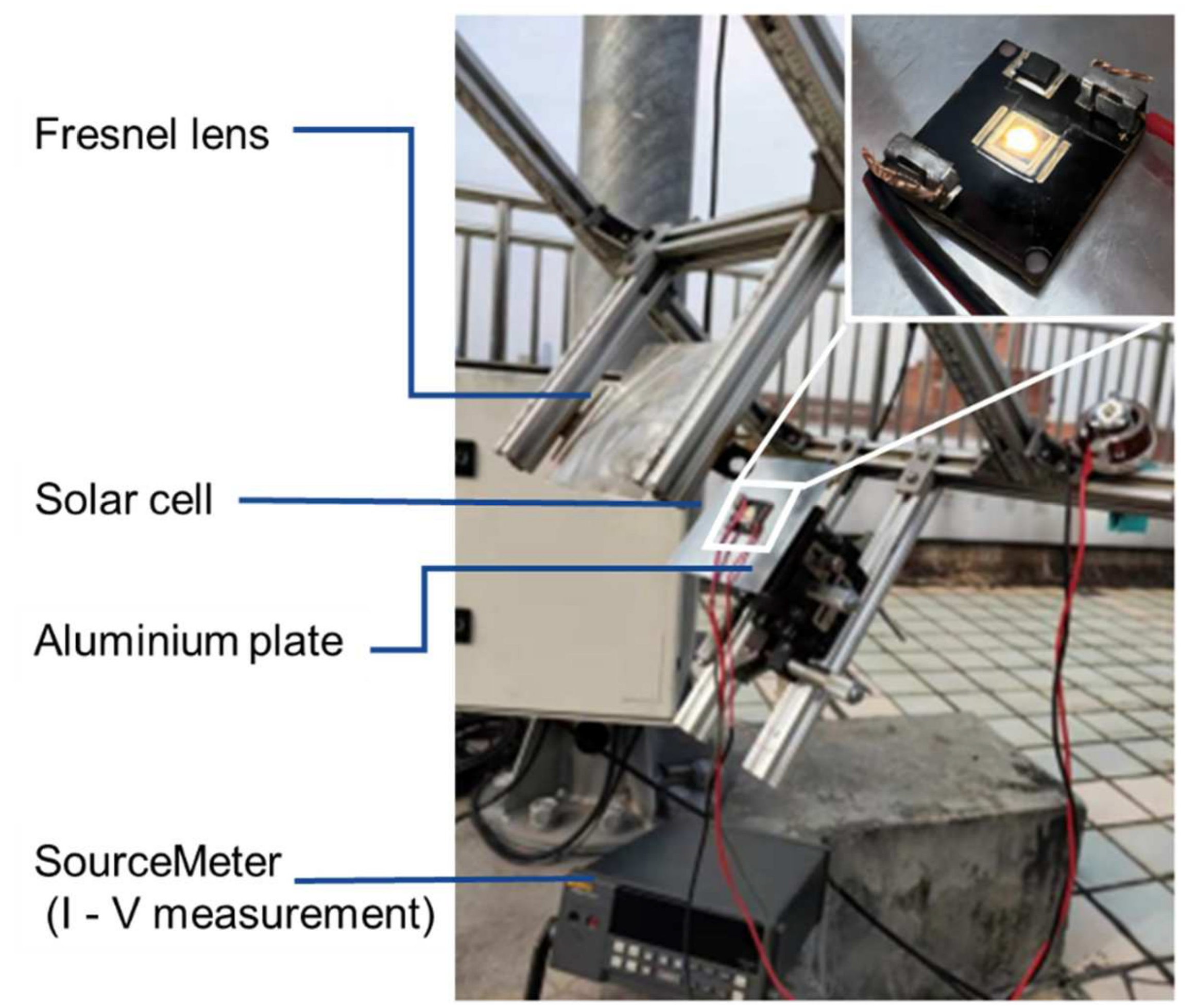
4. Experiment Results

In order to verify the influence of optical–electrical–thermal coupling on the cell along the optical axis, an outdoor experimental platform was built for test and verification. As shown in Figure 12, The experimental equipment is fixed on the sun tracker so that the lens and solar cell front are facing the sun at all times. The solar cell with the focusing spot irradiated on the surface is shown in the insect. The aperture area of the lens is 15,125 mm2 and the focal length is 110 mm. The material of the Fresnel lens is PMMA and the size of the triple-junction cell is 5.5 mm × 5.5 mm in which case the geometric concentration is about 500×.
The experiment was carried out from 12:30 to 13:00 on the top floor of the Solar Energy Research Institute of Sun Yat-sen University in Guangzhou. During this period, the outdoor ambient temperature is around 36 °C. The temperature difference fluctuation is no more than 1 ℃ and the DNI is 830–850   w / m 2 . Moreover, the average wind speed is 1 m/s. The experiment is carried out by adjusting the triaxial displacement table to change the relative distance between the Fresnel lens and the cell. The adjustment range is 10 mm away from the focal plane. The thermocouple for measuring the cell temperature is pasted on the back of the aluminum plate so that the focus incident on the cell surface was not interfered. Under the experimental conditions, the changes in the short-circuit current, open-circuit voltage, filling factor and output power of the triple-junction cell along the optical axis are shown in Figure 13a–d. It can be clearly seen that the short-circuit current decreases by 7.7%, the open circuit voltage decreases from 2.67 v to 2.62 v and the maximum output power decreases by 24%. Table 3 shows the key photovoltaic parameters and cell temperature with the different distances of the cell from the Fresnel. It can be seen that due to the non-uniformity, the output power is minimum near the focal plane and the temperature reaches maximum 63.2 °C, which is 6.4 °C higher than the maximum output power positions (Z = 108 mm). The irradiance and temperature would change slightly in a short time under the outdoor conditions, but the test results are basically consistent with the change trend calculated by the model.

5. Conclusions and Discussion

The non-uniform irradiance, the mismatch between the focusing spectrum and the spectrum of multijunction cell design and the increase in cell temperature are the key factors affecting the photoelectric performance of the multijunction cell. The coupling effect of three factors intensifies its negative impact. Through the optical model, the light intensity and spectral characteristics under the concentration of the Fresnel lens are calculated, and an optical–electrical–thermal coupling model under non-uniform illumination is established to analyze the coupled influence on the cells. The results show that optimizing the placement position of the multijunction cell in the direction of the optical axis can effectively alleviate the negative effects of optical–electrical–thermal coupling caused by non-uniformity of focusing, spectral mismatch and increasing temperature. The main conclusions are as follows:
  • Non-uniformity of concentration: The dispersion effect causes the irradiance concentrated, the spectrum distribution, energy and non-uniformity change significantly at different positions along the optical axis. Moreover, the energy proportion of short, medium and long wavelengths on the cell surface does not change synchronously thus causing the spectrum mismatch (including on the focal plane). For a Z value smaller than the focal distance, the loss of medium and long wavelengths mainly exists. For a Z value larger than the focal distance, the loss of short wavelengths mainly occurs. The non-uniformity of short, medium and long bands is the largest at 110.5 mm, 111.4 mm and 112.3 mm, respectively, and the non-uniformity of all wave bands is the largest at 111.8 mm, which is the result of the synthesis of the three bands.
  • Output performance of multijunction cells: The non-uniformity of the focusing causes the photoelectric performance of the cell placed near the focal plane to decline the most. The optical–electrical–thermal coupling caused by the temperature rise aggravates the negative impact at the focal plane. Based on the numerical analysis of the coupling model and experiments, it was recommended that optimizing the placement position of the multijunction cell in the direction of the optical axis can effectively alleviate the negative effects of optical–electrical–thermal coupling caused by non-uniformity. In the passive heat dissipation condition of 500 times geometric concentration, compared with the cell placed on the on-focus position, the output power of the solar cell placed 2 mm in front of the focal plane increases by 35% and cell temperature decreases by 15%.
The proposed coupled model gives the effects of optical–electrical–thermal coupling on the output performance and the temperature of the multijunction solar cells. However, the simulated value of efficiency decline on the focal plane is higher than those in our experiments. It may result from several factors not modeled, such as the limit of tunneling current of tunnel diodes. However, the coupled effect of multiple physical fields is very common because the non-uniform illumination is a frequent occurrence during the process of power generation. Overall, the simulated trends agree with the experiment result. It can be highlighted that the optical–electrical–thermal coupling effect is strongly affected by non-uniform illumination caused by the dispersion effect. The negative effects caused by non-uniform focusing near the focal plane are exacerbated by the coupled effect, which is caused by the non-uniformity of focusing, spectral mismatch and rising temperature. Therefore, optimizing the distance of the cell on the optical axis is essential for effectively alleviating the negative impact of coupling without extra cost. The choice must be carried out through experimental procedures rather than simulation-only approaches. Further work will focus on the analysis of the coupled effect on a CPV system equipped with secondary optical elements, as well as the analysis of other unavoidable problems of the system such as illumination change caused by sun tracker error.

Author Contributions

Conceptualization, Q.S.; methodology, Q.S.; software, Q.S.; validation, Q.S., J.J. and Y.Z.; formal analysis, Q.S.; investigation, Q.S.; resources, B.S.; data curation, Q.S.; writing—original draft preparation, Q.S.; writing—review and editing, B.S.; visualization, Q.S.; supervision, B.S.; project administration, B.S.; funding acquisition, B.S. All authors have read and agreed to the published version of the manuscript.

Funding

This research was funded by the Natural Science Foundation of Guangdong Province of China, grant number 2021A1515010608, and the National Natural Science Foundation of China, grant number U1707603.

Data Availability Statement

The data presented in this study are available on request from the corresponding author. The data are not publicly available due to privacy.

Conflicts of Interest

The authors declare no conflict of interest. The funders had no role in the design of the study; in the collection, analyses, or interpretation of data; in the writing of the manuscript, or in the decision to publish the results.

References

  1. Shah, A.; Torres, P.; Tscharner, R. Photovoltaic Technology: The Case for Thin-Film Solar Cells. Science 1999, 285, 692–698. [Google Scholar] [CrossRef] [PubMed] [Green Version]
  2. Ferekides, C.S.; Balasubramanian, U.; Mamazza, R.; Viswanathan, V.; Zhao, H.; Morel, D.L. CdTe thin film solar cells: Device and technology issues. Sol. Energy 2004, 77, 823–830. [Google Scholar] [CrossRef]
  3. Ciminelli, C.; Dellrolio, F.; Brunetti, G.; Conteduca, D.; Armenise, M.N. Graphene/Silicon Schottky Junction Solar Cells. In Proceedings of the 2018 20th International Conference on Transparent Optical Networks (ICTON), Bucharest, Romania, 1–5 July 2018. [Google Scholar]
  4. Jin, Y.K.; Lee, J.W.; Jung, H.S.; Shin, H.; Park, N.G. High-Efficiency Perovskite Solar Cells. Chem. Rev. 2020, 120, 7867–7918. [Google Scholar]
  5. Wang, Z.; Song, Z.; Yan, Y.; Liu, S.; Yang, D. Perovskite—A Perfect Top Cell for Tandem Devices to Break the S–Q Limit. Adv. Sci. 2019, 6, 1801704. [Google Scholar] [CrossRef]
  6. Liu, M.; Endo, M.; Shimazaki, A.; Wakamiya, A.; Tachibana, Y. Light Intensity Dependence of Performance of Lead Halide Perovskite Solar Cells. J. Photopolym. Sci. Technol. 2017, 30, 577–582. [Google Scholar] [CrossRef] [Green Version]
  7. Hasan, A.; Sarwar, J.; Shah, A.H. Concentrated photovoltaic: A review of thermal aspects, challenges and opportunities. Renew. Sustain. Energy Rev. 2018, 94, 835–852. [Google Scholar] [CrossRef]
  8. Cotal, H.; Fetzer, C.; Boisvert, J.; Kinsey, G.; King, R.; Hebert, P.; Yoon, H.; Karam, N. III-V multijunction solar cells for concentrating photovoltaics. Energy Environ. Sci. 2009, 2, 174–192. [Google Scholar] [CrossRef]
  9. van Riesen, S.; Neubauer, M.; Boos, A.; Rico, M.M.; Gourdel, C.; Wanka, S.; Krause, R.; Guernard, P.; Gombert, A. New Module Design with 4-Junction Solar Cells for High Efficiencies. In Proceedings of the 11th International Conference on Concentrator Photovoltaic Systems (CPV), Aix les Bains, France, 13–15 April 2015. [Google Scholar]
  10. Green, M.A.; Dunlop, E.D.; Hohl-Ebinger, J.; Yoshita, M.; Kopidakis, N.; Hao, X. Solar cell efficiency tables (version 59). Prog. Photovolt. 2022, 30, 3–12. [Google Scholar] [CrossRef]
  11. Geisz, J.F.; Steiner, M.A.; Jain, N.; Schulte, K.L.; France, R.M.; McMahon, W.E.; Perl, E.E.; Friedman, D.J. Building a Six-Junction Inverted Metamorphic Concentrator Solar Cell. IEEE J. Photovolt. 2018, 8, 626–632. [Google Scholar] [CrossRef]
  12. Baig, H.; Heasman, K.C.; Mallick, T.K. Non-uniform illumination in concentrating solar cells. Renew. Sustain. Energy Rev. 2012, 16, 5890–5909. [Google Scholar] [CrossRef]
  13. Saura, J.M.; Fernandez, E.F.; Almonacid, F.M.; Chemisana, D. Characterisation and impact of non-uniformity on multi-junction solar cells (MJSC) caused by concentrator optics. AIP Conf. Proc. 2019, 2149, 020004. [Google Scholar]
  14. Theristis, M.; O’Donovan, T.S. Electrical-thermal analysis of III-V triple-junction solar cells under variable spectra and ambient temperatures. Sol. Energy 2015, 118, 533–546. [Google Scholar] [CrossRef] [Green Version]
  15. Domenech-Garret, J.-L. Cell behaviour under different non-uniform temperature and radiation combined profiles using a two dimensional finite element model. Sol. Energy 2011, 85, 256–264. [Google Scholar] [CrossRef]
  16. Li, G.; Xuan, Q.; Pei, G.; Su, Y.; Ji, J. Effect of non-uniform illumination and temperature distribution on concentrating solar cell—A review. Energy 2018, 144, 1119–1136. [Google Scholar] [CrossRef]
  17. Baumgartner, H.; Oksanen, B.; Karha, P.; Ikonen, E. Optical Characterization of III-V Multijunction Solar Cells for Temperature-Independent Band Gap Features. IEEE J. Photovolt. 2019, 9, 1631–1636. [Google Scholar] [CrossRef]
  18. Indira, S.S.; Vaithilingam, C.A.; Chong, K.-K.; Saidur, R.; Faizal, M.; Abubakar, S.; Paiman, S. A review on various configurations of hybrid concentrator photovoltaic and thermoelectric generator system. Sol. Energy 2020, 201, 122–148. [Google Scholar] [CrossRef]
  19. Levina, S.A.; Mintairov, M.A.; Filimonov, E.D.; Shvarts, M.Z. Spectral dependencies of multijunction solar cells in a wide range of temperatures. In Proceedings of the International Conference on PhysicA.SPb, Saint Petersburg, Russia, 22–24 October 2019. [Google Scholar]
  20. Cuevas, A.; Lopez-Romero, S. The combined effect of non-uniform illumination and series resistance on the open-circuit voltage of solar cells. Sol. Cells 1984, 11, 163–173. [Google Scholar] [CrossRef]
  21. Mellor, A.; Domenech-Garret, J.L.; Chemisana, D.; Rosell, J.I. A two-dimensional finite element model of front surface current flow in cells under non-uniform, concentrated illumination. Sol. Energy 2009, 83, 1459–1465. [Google Scholar] [CrossRef] [Green Version]
  22. Bunthof, L.A.A.; Haverkamp, E.J.; van der Woude, D.; Bauhuis, G.J.; Corbeek, W.H.M.; Veelenturf, S.; Vlieg, E.; Schermer, J.J. Influence of laterally split spectral illumination on multi junction CPV solar cell performance. Solar Energy 2018, 170, 86–94. [Google Scholar] [CrossRef]
  23. Kumar, N.S.; Matty, K.; Rita, E.; Simon, W.; Ortrun, A.; Alex, C.; Roland, W.; Tim, G.; Kumar, M.T. Experimental validation of a heat transfer model for concentrating photovoltaic system. Appl. Therm. Eng. 2012, 33–34, 175–182. [Google Scholar] [CrossRef]
  24. Lian, R.-H.; Liang, Q.-B.; Shu, B.-F.; Fan, C.; Wu, X.-L.; Guo, Y.; Wang, J.; Yang, Q.-C. Performance and optimization research of triple-junction solar cell along the optical axis direction on the HCPV module. Acta Phys. Sin. 2016, 65. [Google Scholar] [CrossRef]
  25. Steiner, M.; Boesch, A.; Dilger, A.; Dimroth, F.; Doersam, T.; Muller, M.; Hornung, T.; Siefer, G.; Wiesenfarth, M.; Bett, A.W. FLATCON (R) CPV module with 36.7% efficiency equipped with four-junction solar cells. Prog. Photovolt. 2015, 23, 1323–1329. [Google Scholar] [CrossRef]
  26. Li, X.; Lin, G.-J.; Liu, H.-H.; Chen, S.-Y.; Liu, G.-Z. Effect of chromatic aberration on performance of concentrated multi-junction solar cells and their optimization. Acta Phys. Sin. 2017, 66. [Google Scholar] [CrossRef]
  27. Ustun, T.S.; Nakamura, Y.; Hashimoto, J.; Otani, K. Performance analysis of PV panels based on different technologies after two years of outdoor exposure in Fukushima, Japan. Renew. Energy 2019, 136, 159–178. [Google Scholar] [CrossRef]
  28. Zhang, X.-N. Refractive Index Database, Refractive.INFO. Refractive index of (C5H8O2)n (Poly(methyl methacrylate), PMMA)-Zhang-Tomson. 2020. Available online: https://refractiveindex.info/?shelf=organic&book=poly%28methyl_methacrylate%29&page=Zhang-Tomson (accessed on 10 April 2022).
  29. Steiner, M.; Siefer, G.; Hornung, T.; Peharz, G.; Bett, A.W. YieldOpt, a model to predict the power output and energy yield for concentrating photovoltaic modules. Prog. Photovolt. 2015, 23, 385–397. [Google Scholar] [CrossRef]
  30. 3C44A-with 5,5 × 5,55 mm2 Concentrator Triple Junction Solar Cell. 2016. Available online: http://www.azurspace.com/images/products/0004356-00-01_3C44_AzurDesign_5.pdf (accessed on 10 April 2022).
  31. Lv, H.; Sheng, F.; Dai, J.; Liu, W.; Cheng, C.; Zhang, J. Temperature-dependent model of concentrator photovoltaic modules combining optical elements and III-V multi-junction solar cells. Sol. Energy 2015, 112, 351–360. [Google Scholar] [CrossRef]
  32. Steiner, M.; Guter, W.; Peharz, G.; Philipps, S.P.; Dimroth, F.; Bett, A.W. A validated SPICE network simulation study on improving tunnel diodes by introducing lateral conduction layers. Prog. Photovolt. 2012, 20, 274–283. [Google Scholar] [CrossRef]
  33. Lv, H.; Huang, W.; Cheng, C.; Ou, Y.; Liao, J.; Su, Y.; Riffat, S. An improved model to predict thermal runaway in concentrator III-V multi-junction solar cells. Int. J. Low-Carbon Technol. 2018, 13, 432–437. [Google Scholar] [CrossRef]
  34. Maka, A.O.M.; O’Donovan, T.S. Transient thermal-electrical performance modelling of solar concentrating photovoltaic (CPV) receiver. Sol. Energy 2020, 211, 897–907. [Google Scholar] [CrossRef]
  35. Espinet, P.; Garcia, I.; Rey-Stolle, I.; Algora, C.; Baudrit, M. Extended description of tunnel junctions for distributed modeling of concentrator multi-junction solar cells. Sol. Energy Mater. Sol. Cells 2011, 95, 2693–2697. [Google Scholar] [CrossRef] [Green Version]
  36. Araki, K.; Uozumi, H.; Yamaguchi, M.; Ieee, I. A simple-passive cooling structure and its heat analysis for 500 X concentrator PV module. In Proceedings of the Conference Record of the Twenty-Ninth Ieee Photovoltaic Specialists Conference 2002, New Orleans, LA, USA, 19–24 May 2002; pp. 1568–1571. [Google Scholar]
  37. Maka, A.O.M.; O’Donovan, T.S. A review of thermal load and performance characterisation of a high concentrating photovoltaic (HCPV) solar receiver assembly. Sol. Energy 2020, 206, 35–51. [Google Scholar] [CrossRef]
  38. Abo-Zahhad, E.M.; Ookawara, S.; Radwan, A.; El-Shazly, A.H.; El-Kady, M.F.; Esmail, M.F.C. Performance, limits, and thermal stress analysis of high concentrator multijunction solar cell under passive cooling conditions. Appl. Therm. Eng. 2020, 164, 114497. [Google Scholar] [CrossRef]
  39. An, Y.; Sheng, C.; Li, X. Radiative cooling of solar cells: Opto-electro-thermal physics and modeling. Nanoscale 2019, 11, 17073–17083. [Google Scholar] [CrossRef] [PubMed]
  40. Araki, K.; Yamaguchi, M. Extended distributed model for analysis of non-ideal concentration operation. Sol. Energy Mater. Sol. Cells 2003, 75, 467–473. [Google Scholar] [CrossRef]
  41. Zhu, L.; Kim, C.; Yoshita, M.; Chen, S.Q.; Sato, S.; Mochizuki, T.; Akiyama, H.; Kanemitsu, Y. Impact of sub-cell internal luminescence yields on energy conversion efficiencies of tandem solar cells: A design principle. Appl. Phys. Lett. 2014, 104, 031118. [Google Scholar] [CrossRef]
  42. Helmers, H.; Schachtner, M.; Belt, A.W. Influence of temperature and irradiance on triple-junction solar subcells. Sol. Energy Mater. Sol. Cells 2013, 116, 144–152. [Google Scholar] [CrossRef]
  43. Gopal, R.; Dwivedi, R.; Srivastava, S.K. Effect of nonuniform illumination on the photovoltaic decay characteristic of solar cells. IEEE Trans. Electron Devices 1986, ED-33, 802–809. [Google Scholar] [CrossRef]
  44. Garcia, I.; Rey-Stolle, I.; Galiana, B.; Algora, C. A 32.6% efficient lattice-matched dual-junction solar cell working at 1000 suns. Appl. Phys. Lett. 2009, 94, 053509. [Google Scholar] [CrossRef]
Figure 1. (a) The structure of the concentrating photovoltaic cell. (b) The geometrical relationships between the incident light and the refracted light.
Applsci 12 05888 g001
Figure 2. (a) GaInP/GaInAs/Ge triple-junction solar cell; (b) Double diode circuit network model.
Applsci 12 05888 g002
Figure 3. Heat dissipation diagram of the receiver.
Applsci 12 05888 g003
Figure 4. (a) Optical efficiency at different optical axis positions (in the range of 300–1700 nm); (b) Radiation power at different positions in the optical axis direction.
Applsci 12 05888 g004
Figure 5. Light spot distribution on the cell surface. (a) Z = 108 mm; (b) Z = 109 mm; (c) Z = 110 mm (focal plane); (d) Z = 111 mm; (e) Z = 112 mm; (f) Z = 114 mm.
Applsci 12 05888 g005
Figure 6. Surface temperature distribution of the receiver. (a) Z = 108 mm; (b) Z = 109 mm; (c) Z = 110 mm (focal plane); (d) Z = 111 mm; (e) Z = 112 mm; (f) Z = 114 mm.
Applsci 12 05888 g006
Figure 7. Variation in cell characteristic parameters in the direction of optical axis: (a) short-circuit current; (b) open-circuit voltage; (c) filling factor; (d) maximum output power.
Applsci 12 05888 g007
Figure 8. Photogenerated current density in the cell width direction at different optical axis positions. (a) Z = 108 mm; (b) Z = 109 mm; (c) Z = 110 mm (focal plane); (d) Z = 111 mm; (e) Z = 112 mm; (f) Z = 114 mm.
Applsci 12 05888 g008
Figure 9. (a) Short-circuit current of three sub cells; (b) Minimum short-circuit current of sub cells and short-circuit current of triple-junction solar cell.
Applsci 12 05888 g009
Figure 10. (a) Open-circuit voltage of three sub cells; (b) Open-circuit voltage of sub cells and open-circuit voltage of triple-junction solar cell.
Applsci 12 05888 g010
Figure 11. Open-circuit voltage at different optical axis positions. (a) InGaP sub cell; (b) InGaAs sub cell; (c) Ge sub cell; (d) Triple-junction solar cell.
Applsci 12 05888 g011
Figure 12. Outdoor performance test of the triple-junction solar cell. The insect shows the solar cell with the focusing spot irradiated on the surface.
Applsci 12 05888 g012
Figure 13. Variation in output parameters in the optical axis direction. (a) Short-circuit current; (b) Open-circuit voltage; (c) Filling factor; (d) Output power.
Applsci 12 05888 g013
Table 1. Parameters of each layer material of the receiver.
CategoryThickness (mm)Length (mm)Width (mm)
Cell0.195.55.5
DBC upper layer0.252325
DBC ceramic layer0.3224.526.5
DBC lower layer0.252426
Aluminum heat spreader0.69090
Table 2. The optical axis position of the maximum peak-to-average ratio (PAR) of different wavelengths.
Maximum PAROptical Axis Position of Maximum Par (Z)
short wavelengths (300–700 nm)55.5110.5 mm
middle wavelengths (700–900 nm)67.4111.4 mm
long wavelengths (900–1700 nm)74.8112.3 mm
all wavelengths (300–1700 nm)64.1111.8 mm
Table 3. The output performance and temperature of the cell at different positions of the optical axis.
Distance of the Cell
from the Fresnel (mm)
108 110112 114 116
T c e l l   ( ° C )56.862.263.258.251.9
I s c   (A)0.9570.9240.9430.9730.821
V o c (V)2.6562.6362.6212.6452.667
F F   0.7830.7260.6170.6870.777
P m a x (W)1.9901.7691.5291.7671.702
Publisher’s Note: MDPI stays neutral with regard to jurisdictional claims in published maps and institutional affiliations.

