Article

A Ku-Band Bi-Directional Transmit and Receive IC in 0.13 μm CMOS Technology

1
Department of Electronic Engineering, Kwangwoon University, Seoul 01897, Korea
2
School of Electrical Engineering, Chung-Ang University, Seoul 06974, Korea
*
Author to whom correspondence should be addressed.
Appl. Sci. 2022, 12(11), 5710; https://doi.org/10.3390/app12115710
Submission received: 10 May 2022 / Revised: 31 May 2022 / Accepted: 1 June 2022 / Published: 3 June 2022
(This article belongs to the Special Issue Recent Research in Microwave and Millimeter-Wave Components)

Abstract

:
This paper presents a Ku-band transmit and receive IC in 0.13 µm CMOS technology for mobile satellite communication beamforming systems. A Ku-band transmit and receive IC is composed of a bi-directional amplifier, a 6-bit phase shifter, and a 6-bit digital step attenuator. The precise trimming bits are implemented in the phase shifter (2.8°) and digital step attenuator (0.5 and 1 dB) for the amplitude and phase error correction. The phase variation range of the phase shifter is 360° with a phase resolution of 5.625°. The attenuation range of 31.5 dB with an amplitude resolution of 0.5 dB is achieved. The gain of 2~5 dB and the input/output return losses of >10 dB are achieved from 12 to 16 GHz. The chip size is 2.5 × 1.5 mm2 including bonding pads. The DC power consumption is 216 mW.

1. Introduction

A Ku-band transmit and receive IC is one of the key components in active phased array antennas for Ku-band satellite communications [1,2]. The silicon technology in phased array antennas is receiving attention because it allows for low size, weight, power, and cost (SWAP-C) implementation [3]. Separate phase shifters and gain control circuits for transmit and receive operations are typically used to implement the transmit and receive IC for the phased array antenna [4]. However, it occupies a large chip area and results in high manufacturing costs. The chip size can be decreased significantly using bi-directional topology, sharing the Tx and Rx chains with phase shifters and attenuators [5,6,7]. One disadvantage of the bi-directional topology is that it results in an additional loss of two SPDT switches. A Ku-band transmit and receive IC is composed of a switchless bi-directional amplifier to reduce the losses caused by two SPDT switches. The previous paper composed each test circuit for a phased array antenna in the X band to verify the proposed topology [5,6,7]. Many research groups have already published phase shifters with various circuit topologies [8,9,10,11,12]. The vector sum or the switched filter phase shifter circuit topologies are popularly used. A compact size with decent gain, precise phase control, and wide bandwidth can be achieved in the vector sum phase shifter. However, it has relatively poor linearity and only operates unidirectionally. It also consumes DC current, whereas the switched filter phase shifter can provide high linearity with nearly zero DC power consumption. It operates bidirectionally due to the passive circuit. The digital step attenuator is necessary to control the antenna sidelobe level. The amplitude errors among the elements in the phased array antenna can be compensated.
In this paper, a transmit and receive IC for a Ku-band phased array antenna is presented with 0.13 μm CMOS technology.

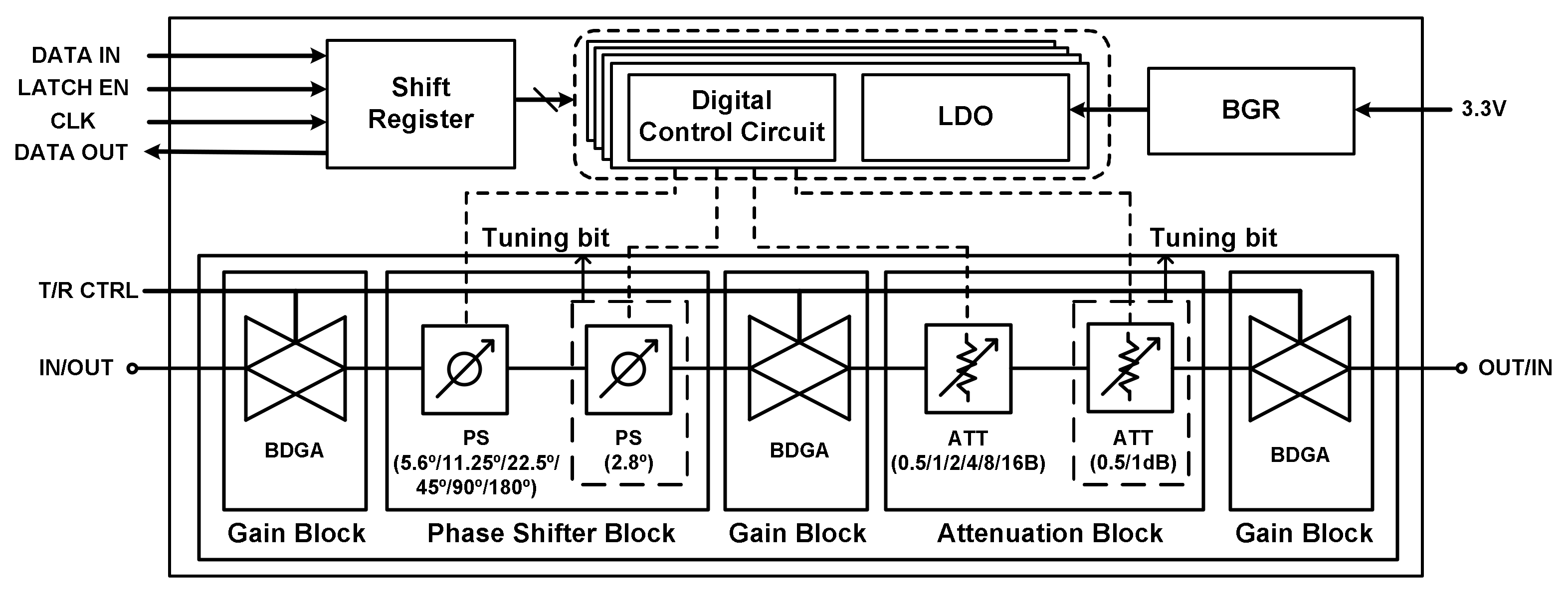
2. Design of Ku-Band Bi-Directional Transmit and Receive IC

Figure 1 shows a block diagram of a Ku-band bi-directional CMOS transmit and receive IC. The transmit and receive IC is composed of a bi-directional amplifier, a 6-bit phase shifter, and a 6-bit digital step attenuator. The phase shifter and attenuator are composed of DPDT switches. Since the series transistors in the switches determine the insertion losses of the phase shifter or the attenuator, the number of the cascaded series transistors should be reduced. The phase shifter or the attenuator with DPDT switches can reduce the number of the series transistors compared to the control circuits only with SPDT switches, which results in improving the insertion loss. In this design, the phase shifter and the attenuator are split with bi-directional amplifiers to improve linearity. A serial peripheral interface (SPI) is implemented to control the state registers of the phase and attenuation, and a low dropout (LDO) voltage regulator is also integrated to provide the stable DC bias.

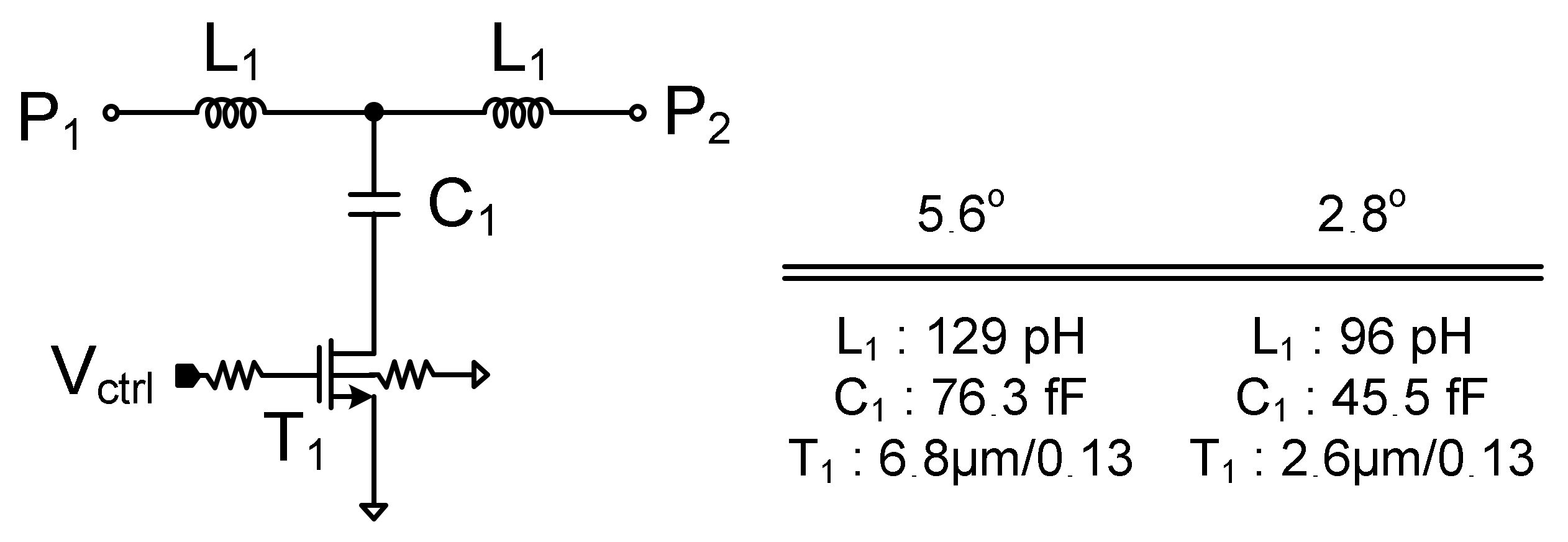
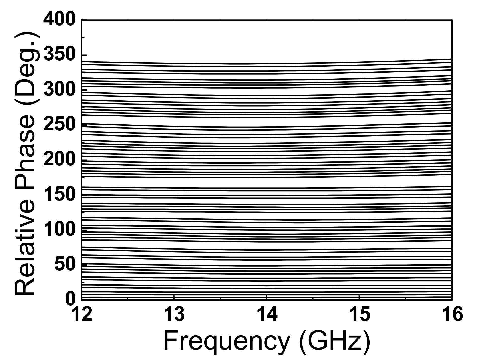
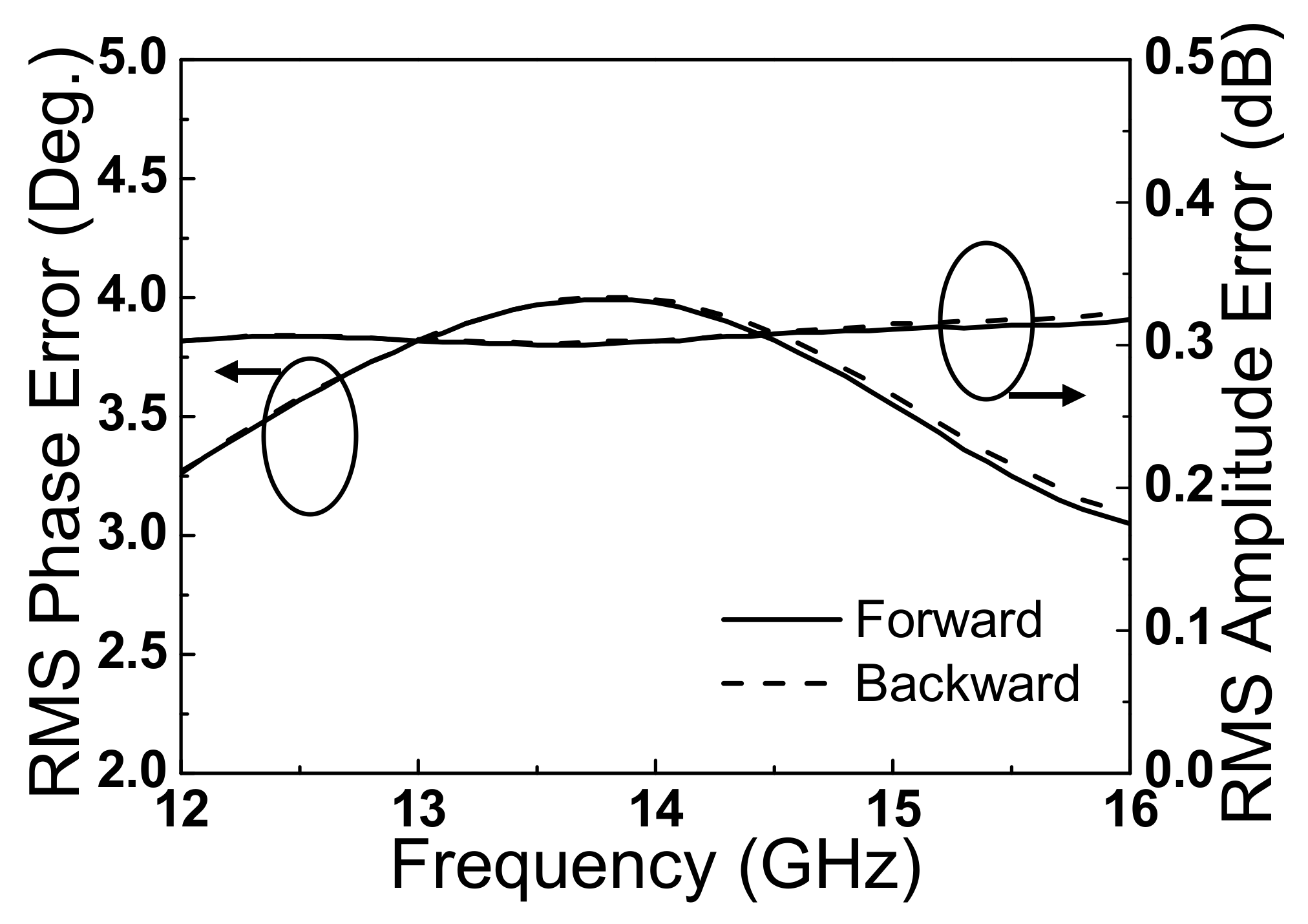
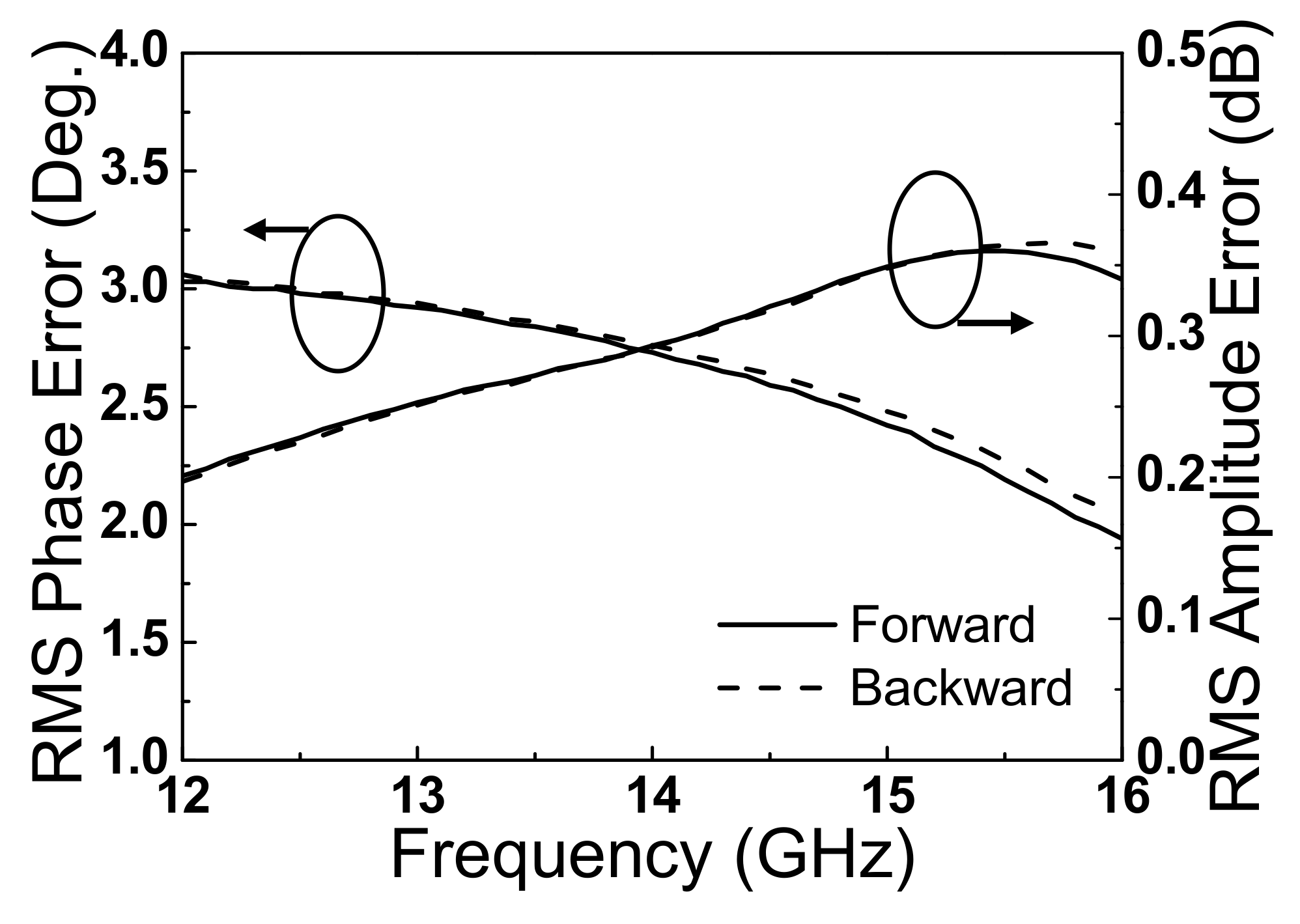
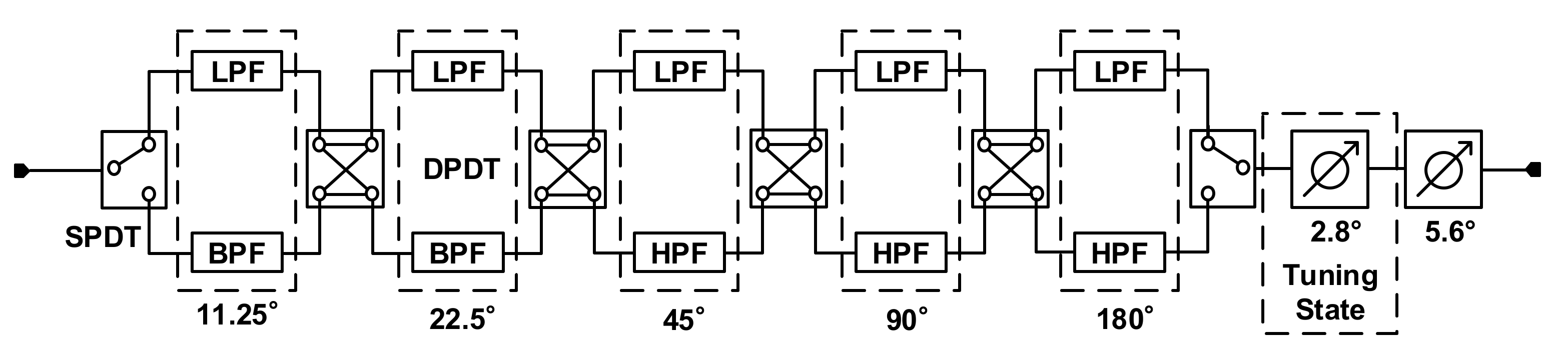
2.1. Ku-Band 6-Bit Phase Shifter

Figure 2 shows the circuit block diagram of a Ku-band 6-bit phase shifter with DPDT switches. The DPDT switch with a series–shunt circuit is designed to provide high port-to-port isolation. Figure 3 shows the schematic of the SPDT and DPDT switches. The DPDT switch is implemented with four 16-finger 64 μm series transistors (T1–T4) and four 8-finger 40 μm shunt transistors (T5–T8). The series inductors (L1) of 260 pH improve the input and the output return losses. The filter type phase shifting circuits are implemented in Figure 4. In the 11.25° and 22.5° phase states, BPF and LPF networks are used. Since a large shunt inductance is necessary to implement 11.25° and 22.5° phase states, the BPF with small series inductance is used to reduce the chip size. In the 45° and 90° phase states, HPF and LPF networks are used. To provide the wideband operation, two stages of HPF and LPF networks are used in the180° phase state. Table 1 summarizes the design parameters of the switched filter phase shifter. The 5.625° phase state and the 2.8° phase tuning bit are implemented with the switched LPF in Figure 5. The body floating technique is used in the switches to reduce the silicon substrate leakage. Vertically stacked spiral inductors are used to reduce the chip size. All the passive devices such as inductors, MIM capacitors, and interconnection lines were designed using the electromagnetic simulator.

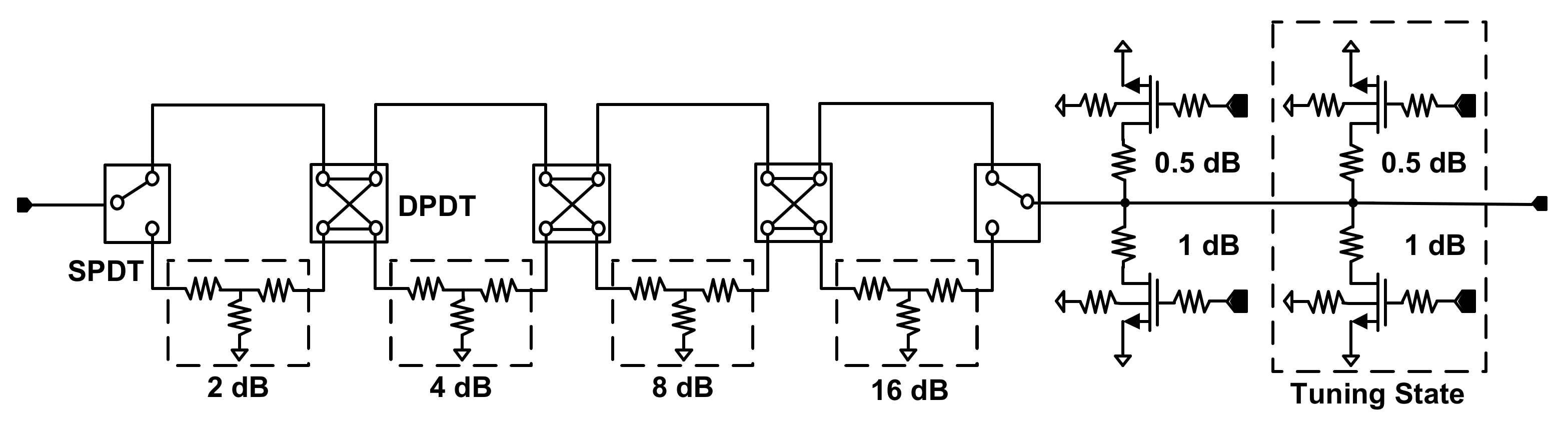
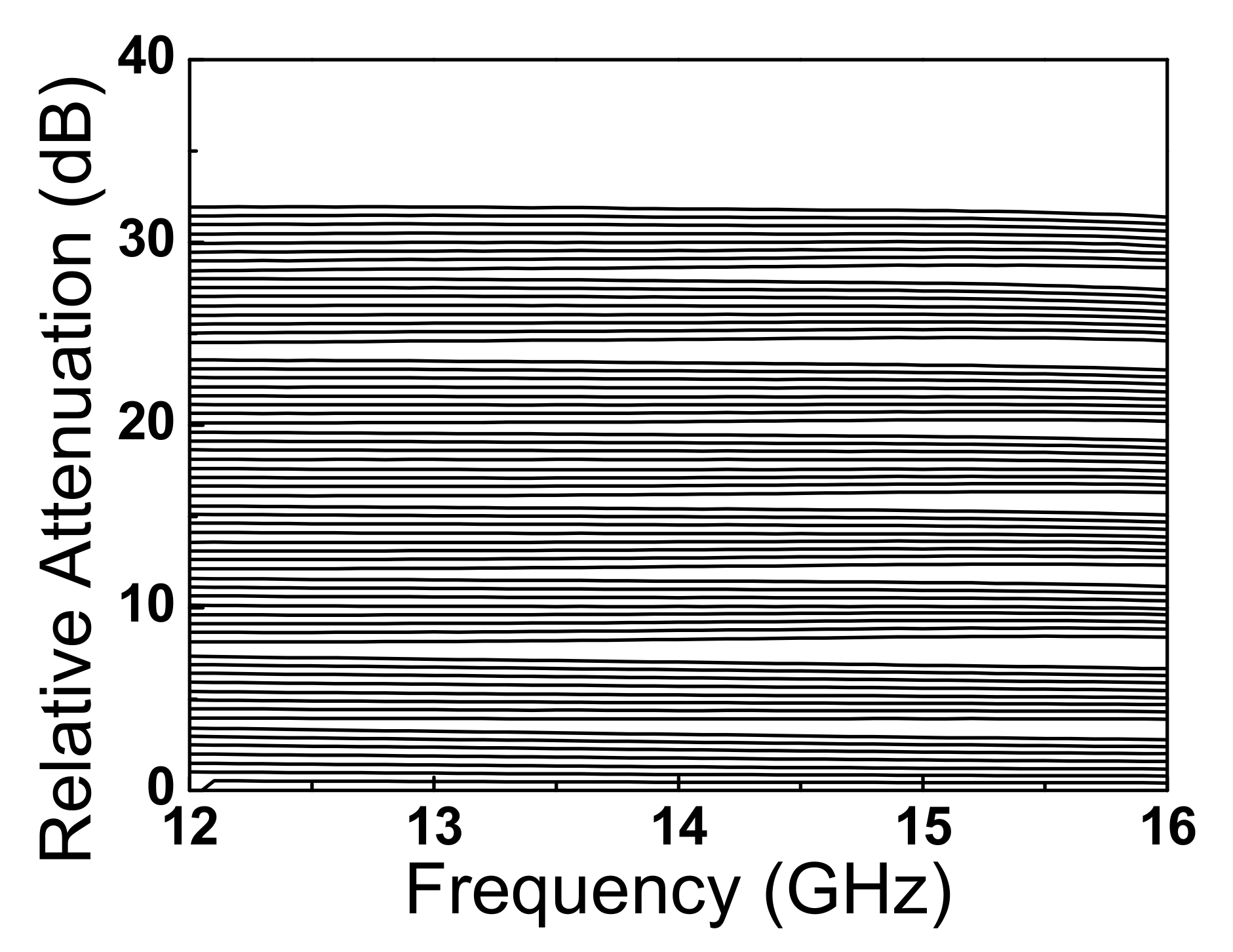
2.2. Ku-Band 6-Bit Digital Step Attenuator

The block diagram of the Ku-band 6-bit digital step attenuator is shown in Figure 6. The attenuator is designed with T-type resistive networks. The attenuation steps of 2, 4, 8, and 16 dB are controlled by steering the signal paths between the reference paths and the T-shape resistive network path using the DPDT switches. The 0.5 and 1 dB attenuation states are designed with a switched shunt resistor to reduce the insertion loss and chip size. Additionally, the 0.5 and 1 dB attenuation states are designed as tuning bits to compensate for the amplitude error. The attenuation variation range is 31.5 dB with an attenuation resolution of 0.5 dB.

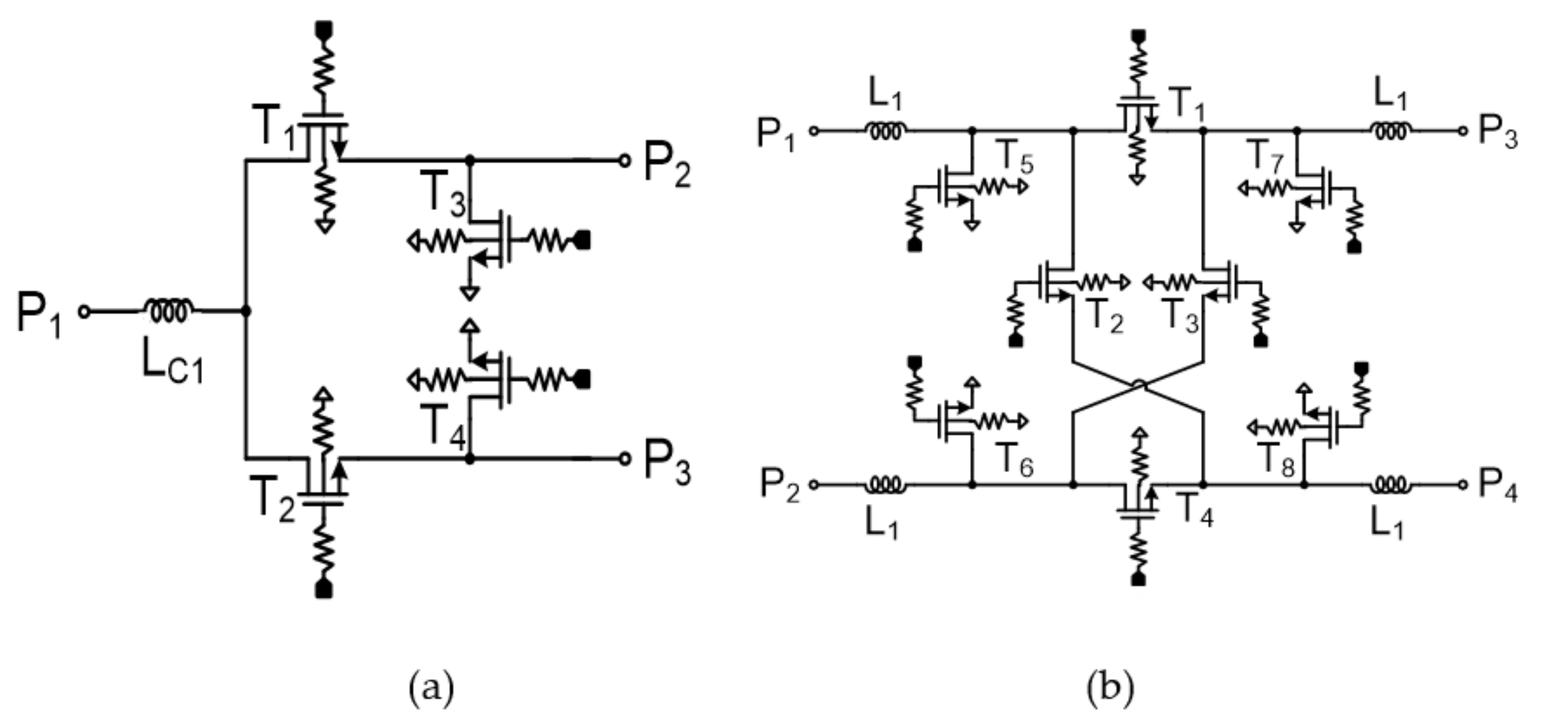
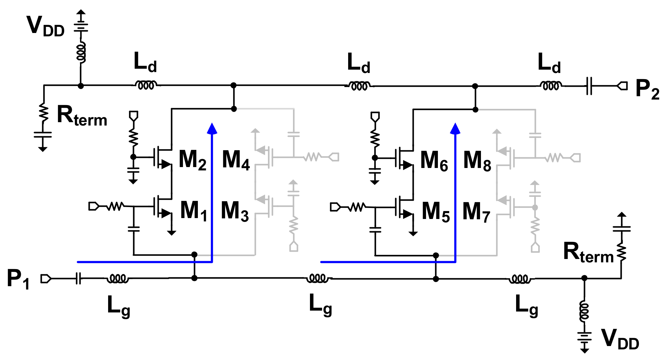
2.3. Switchless Bi-Directional Amplifier

The bi-directional amplifier in the transmit and receive IC for the phased array antenna is generally implemented with two SPDT switches, an LNA, and a PA. Two SPDT switches for the bi-directional operation result in an additional loss and a larger chip size. Figure 7 shows the schematic of the proposed bi-directional amplifier. The switchless bi-directional amplifier is composed of a paired two-stage distributed cascode amplifier. Since the transmit and receive switching operation is provided by switching the cascode transistors in the proposed amplifier, the small size can be achieved by removing the two transmit and receive SPDT switches. In the receive operation from P1 to P2, the transistors of M1/M5 and M2/M6 are in ON states and the transistors of M3/M7 and M4/M8 are in OFF states. Therefore, it works equivalently as a distributed amplifier. The transmit operation is vice versa. Generally, the insertion losses in the control circuits have a negative slope versus the frequencies, and so the amplifier is designed to have a positive gain slope. Flat overall gain performance can be achieved in the Ku-band transmit and receive IC. The symmetric layout was performed for identical operational characteristics in the transmit and receive operation modes.

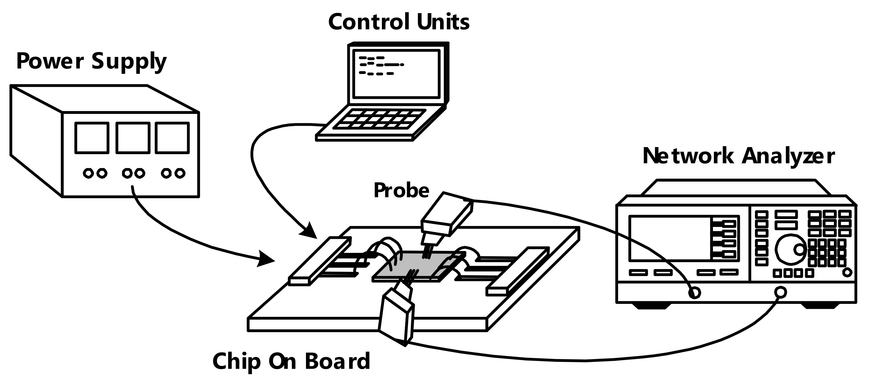
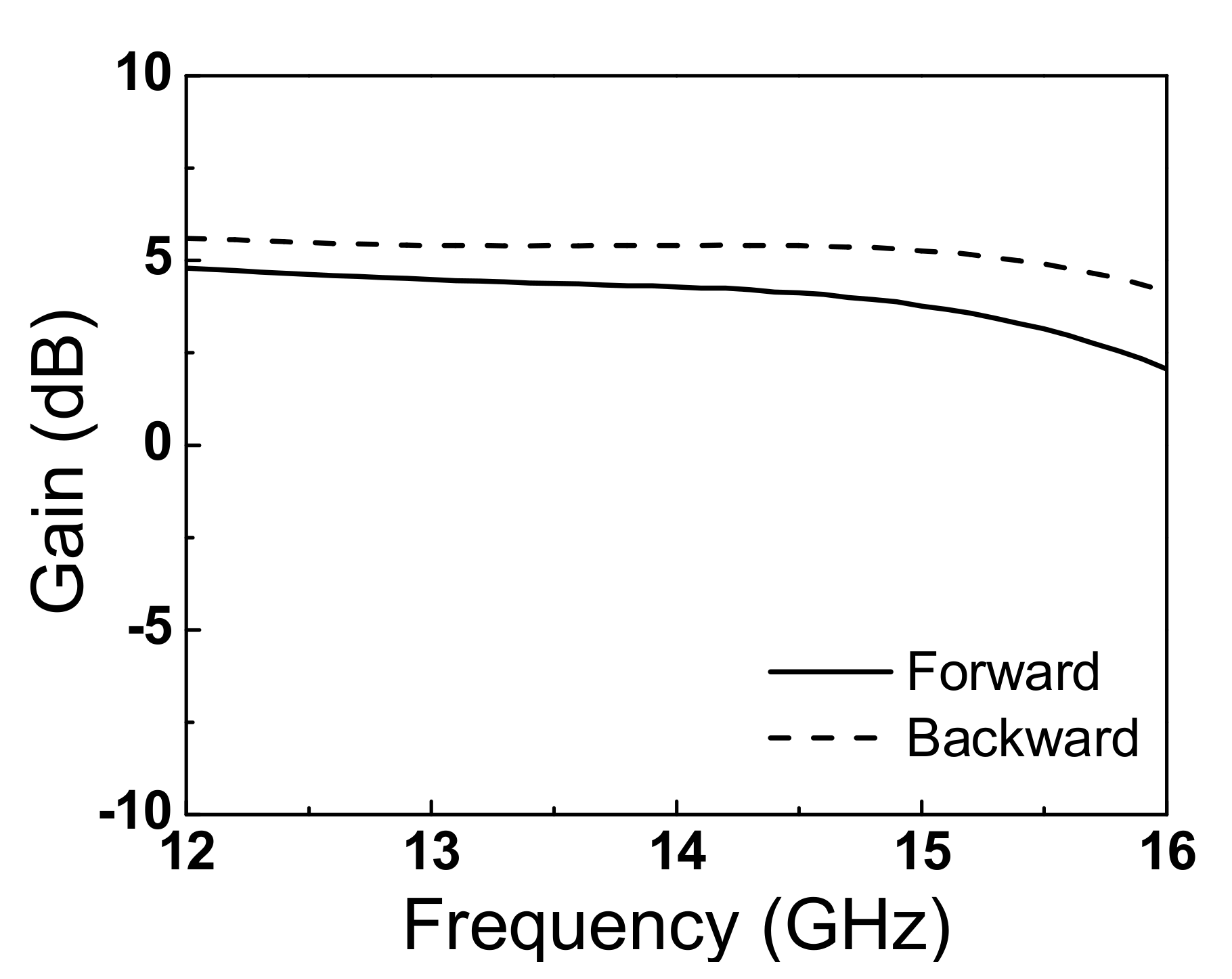
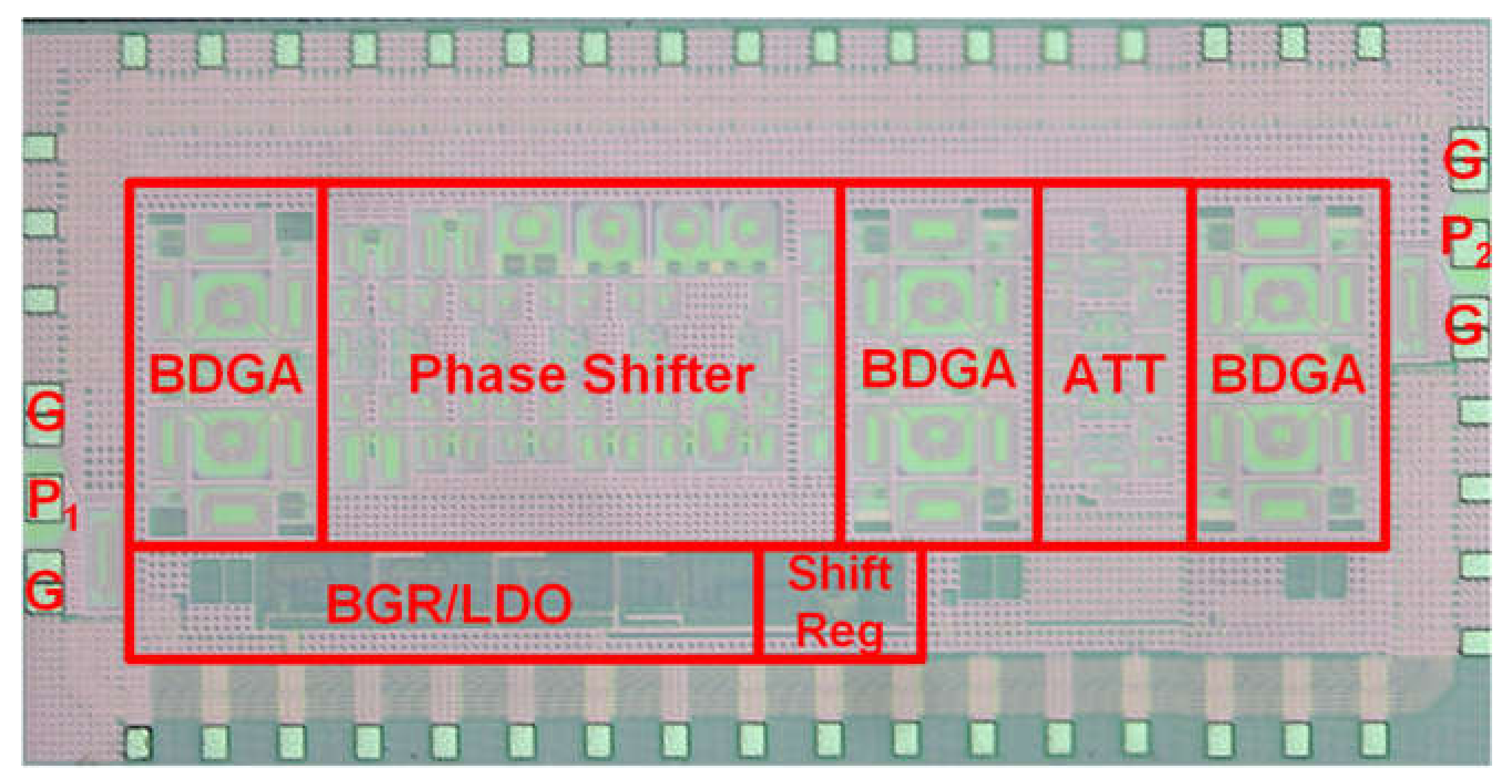
3. Experiment Results

The Ku-band transmit and receive IC is fabricated in 0.13 μm CMOS technology and the chip size is 2.5 × 1.5 mm2 including bonding pads. The microphotograph of the Ku-band CMOS transmit and receive IC is shown in Figure 8. The measurement setup of the Ku-band CMOS transmit and receive IC is shown in Figure 9. The S-parameter measurement is performed using a PNA-X network analyzer. The short, open, load, and thru (SOLT) calibration was performed with the on-wafer probe station. The power characteristics are measured with the signal source and the spectrum analyzer. Figure 10 shows the measured gain of the reference state. The gain is 2~5 dB at 12–16 GHz. The input and output return losses are >10 dB at 12–16 GHz as shown in Figure 11. Figure 12 shows the measured phase characteristics in all phase states. A phase variation range of 360° with a phase resolution of 5.625° is achieved. Figure 13 shows the measured attenuation characteristics in all attenuation states, and an attenuation range of 31.5 dB with an attenuation resolution of 0.5 dB is achieved at 12–16 GHz. As shown in Figure 14, the measured root mean square amplitude error is <0.3 dB and the root mean square phase error is <4° at 12–16 GHz when varying the phase states. Figure 15 shows that the measured root mean square amplitude error is <0.4 dB and the root mean square phase error is <3° at 12–16 GHz when varying the attenuator states. Figure 16 shows the measured power characteristics. The saturated output power is ~2 dBm at 14 GHz. A performance comparison of the previously published silicon-based transmit and receive ICs is summarized in Table 2.

4. Conclusions

This paper presents a Ku-band CMOS transmit and receive IC in 0.13 μm CMOS technology, which is the key part of the phased array antenna for mobile satellite communication beamforming systems. It is proposed to enable the bi-directional amplifier without switches to compensate for the gain, phase shifting for beam steering, and attenuating for weighting technique to reduce the side lobe level. The maximum phase shift range of 360° with a phase resolution of 5.625° and the maximum attenuation range of 31.5 dB with an attenuation resolution of 0.5 dB is achieved. The measured gain is 2~5 dB and the input and output return losses are >10 dB at 12–16 GHz. The saturated output power is −2 dBm at 14 GHz. The chip size is 2.5 × 1.5 mm2 including bonding pads. The total power consumption is 216 mW. The proposed Ku-band CMOS transmit and receive IC will enable the low SWAP-C Ku-band satellite communication and radar system.

Author Contributions

Conceptualization, D.B. and J.-G.K.; methodology, D.B. and J.-G.K.; investigation, D.B. and J.-G.K.; writing—original draft preparation, D.B. and J.-G.K.; writing—review and editing, D.B. and J.-G.K.; supervision, D.B.; project administration, D.B. and J.-G.K.; funding acquisition, J.-G.K. All authors have read and agreed to the published version of the manuscript.

Funding

This work has been supported by the Nano UAV Intelligence Systems Research Laboratory program of Defense Acquisition Program Administration and Agency for Defense Development (UD200027ED).

Institutional Review Board Statement

Not applicable.

Informed Consent Statement

Not applicable.

Data Availability Statement

The data can be obtained from the authors on request.

Conflicts of Interest

The authors declare no conflict of interest.

References

  1. Encinar, J.; Arrebola, M.; Fuenten, L.; Toso, G. Transmit-receive reflectarray antenna for direct broadcast satellite applications. IEEE Trans. Antennas Propag. 2011, 59, 3255–3264. [Google Scholar] [CrossRef]
  2. Baggen, R.; Vaccaro, S.; Rio, D.; Padilla, J. Small-scale prototype of a Ku-band phased array for mobile satellite communications. In Proceedings of the IEEE-APS Conference on Antennas and Propagation for Wireless Communications, Torino, Italy, 12–16 September 2011; pp. 491–494. [Google Scholar]
  3. Kang, D.; Kim, J.; Min, B.; Rebeiz, G. Single and four-element Ka-band transmit/receive phased-array silicon RFICs with 5-bit amplitude and phase control. IEEE Trans. Microw. Theory Tech. 2009, 57, 3534–3543. [Google Scholar] [CrossRef]
  4. Saha, P.; Muralidharan, S.; Cao, J.; Gurbuz, O.; Hay, C. X/Ku-Band Four-Channel Transmit/Receive SiGe Phased-Array IC. In Proceedings of the 2019 IEEE Radio Frequency Integrated Circuits Symposium Digest, Boston, MA, USA, 2–4 June 2019. [Google Scholar]
  5. Cho, M.; Yoon, S.; Sim, S.; Jeon, L.; Kim, J. CMOS-based bi-directional T/R chipsets for phased array antenna. In Proceedings of the 2012 IEEE/MTT-S International Microwave Symposium Digest, Montreal, QC, Canada, 17–22 June 2012. [Google Scholar]
  6. Cho, M.; Han, J.; Kim, J.; Kim, J. An X/Ku-band bi-directional true time delay T/R chipset in 0.13 µm CMOS technology. In Proceedings of the 2014 IEEE/MTT-S International Microwave Symposium Digest, Tampa, FL, USA, 1–6 June 2014. [Google Scholar]
  7. Nguyen, V.-V.; Nam, H.; Choe, Y.J.; Lee, B.-H.; Park, J.-D. An X-band Bi-Directional Transmit/Receive Module for a Phased Array System in 65-nm CMOS. Sensors 2018, 18, 2569. [Google Scholar] [CrossRef] [PubMed] [Green Version]
  8. Hieda, M.; Miyaguchi, K.; Kurusu, H.; Ikematsu, H.; Iyama, Y.; Takagi, T.; Ishida, O. A compact Ku-band 5-bit MMIC phase shifter. IEICE Trans. Electron. 2003, E86-C, 2437–2444. [Google Scholar]
  9. Koh, K.; Rebeiz, G. 0.13 μm CMOS phase shifters for X-, Ku-, and K-band phased arrays. IEEE J. Solid-State Circuits 2007, 42, 2535–2546. [Google Scholar] [CrossRef] [Green Version]
  10. Kang, D.; Lee, H.; Kim, C.; Hong, S. Ku-Band MMIC Phase Shifter Using a Parallel Resonator with 0.18-μm CMOS Technology. IEEE Trans. Microw. Theory Tech. 2006, 54, 294–301. [Google Scholar] [CrossRef]
  11. Morton, M.; Papapolymerou, J. 5 bit silicon-based X-band phase shifter using a hybrid pi/t high-pass/low-pass topology. IET Microw. Antennas Propag. 2008, 2, 19–22. [Google Scholar] [CrossRef]
  12. Wang, L.; Sun, P.; You, Y.; Mikul, A.; Bonebright, R.; Kromholtz, G.; Heo, D. Highly linear Ku-band SiGe PIN diode phase shifter in standard SiGe BiCMOS process. IEEE Microw. Wirel. Compon. Lett. 2010, 20, 37–39. [Google Scholar] [CrossRef]
Figure 1. Block diagram of the Ku-band CMOS transmit and receive IC.
Applsci 12 05710 g001
Figure 2. Block diagram of the Ku-band 6-bit phase shifter.
Applsci 12 05710 g002
Figure 3. Schematics of (a) the SPDT switch, and (b) the DPDT switch.
Applsci 12 05710 g003
Figure 4. Schematics of the phase shifting elements of (a) 11.25° and 22.5°, (b) 45° and 90°, (c) 180°.
Applsci 12 05710 g004
Figure 5. Schematic of the phase shifting elements of 5.6° and 2.8°.
Applsci 12 05710 g005
Figure 6. Block diagram of the Ku-band 6-bit digital step attenuator.
Applsci 12 05710 g006
Figure 7. Schematic of the switchless bi-directional amplifier (operation mode: P1->P2).
Applsci 12 05710 g007
Figure 8. Microphotograph of the Ku-band CMOS transmit and receive IC.
Applsci 12 05710 g008
Figure 9. Measurement setup of the Ku-band CMOS transmit and receive IC.
Applsci 12 05710 g009
Figure 10. Measured gain of the Ku-band CMOS transmit and receive IC.
Applsci 12 05710 g010
Figure 11. Measured return losses of the Ku-band CMOS transmit and receive IC.
Applsci 12 05710 g011
Figure 12. Measured phase characteristics of the Ku-band CMOS transmit and receive.
Applsci 12 05710 g012
Figure 13. Measured attenuation characteristics of the Ku-band CMOS transmit and receive.
Applsci 12 05710 g013
Figure 14. Measured root mean square phase and amplitude errors of the phase shifter.
Applsci 12 05710 g014
Figure 15. Measured RMS phase and amplitude errors of the attenuator.
Applsci 12 05710 g015
Figure 16. Measured output power of the Ku-band CMOS transmit and receive IC in Tx operation.
Applsci 12 05710 g016
Table 1. Design parameters of the phase shifting filter networks.
Parameter11.25° 22.5° 45° 90° 180°
HPF
(BPF)
L1 (pH)1772211420898915
C2 (pF)1.20.572.10.620.62
LPFL2 (pH)156229176287287
C2 (fF)74118102146146
Table 2. Performance comparison of the relevant silicon-based transmit and receive IC.
Reference[4][6][7]This Work
Frequency (GHz)8–168–10.58–10.512–16
TechnologySiGe 0.18 μmCMOS 0.13 μmCMOS 65 nmCMOS 0.13 μm
Rx/Tx Gain (dB)10~16/15~213.5/3.53.7/3.72~5/2~5
Phase shifter range/step (Deg.)360/2.8360/5.625360/5.625360/5.625
Gain control range/step (dB)31/0.531.5/131.5/0.531.5/0.5
RMS Phase Error (Deg.)2.84.344
RMS Phase Error (Deg.)0.30.30.50.5
Psat (dBm)139.5102 @ 14 GHz
Rx/Tx Power consumption (mW)215/280150/150170/170216/216
Chip size (mm2)161.199.563.75
Publisher’s Note: MDPI stays neutral with regard to jurisdictional claims in published maps and institutional affiliations.

