Abstract
Silicon wafers are crucial for determining the price of solar cell modules. To reduce the manufacturing cost of photovoltaic devices, the thicknesses of wafers are reduced. However, the conventional module manufacturing method using the tabbing process has a disadvantage in that the cell is damaged because of the high temperature and pressure of the soldering process, which is complicated, thus increasing the process cost. Consequently, when the wafer is thinned, the breakage rate increases during the module process, resulting in a lower yield; further, the module performance decreases owing to cracks and thermal stress. To solve this problem, a module manufacturing method is proposed in which cells and wires are bonded through the lamination process. This method minimizes the thermal damage and mechanical stress applied to solar cells during the tabbing process, thereby manufacturing high-power modules. When adopting this method, the front electrode should be customized because it requires busbarless solar cells different from the existing busbar solar cells. Accordingly, the front electrode was designed using various simulation programs such as Griddler 2.5 and MathCAD, and the effect of the diameter and number of wires in contact with the front finger line of the solar cell on the module characteristics was analyzed. Consequently, the efficiency of the module manufactured with 12 wires and a wire diameter of 0.36 mm exhibited the highest efficiency at 20.28%. This is because even if the optical loss increases with the diameter of the wire, the series resistance considerably decreases rather than the loss of the short-circuit current, thereby improving the fill factor. The characteristics of the wire-embedded ethylene vinyl acetate (EVA) sheet module were confirmed to be better than those of the five busbar tabbing modules manufactured by the tabbing process; further, a high-power module that sufficiently compensated for the disadvantages of the tabbing module was manufactured.
1. Introduction
Crystalline silicon (c-Si) wafers, a key element of solar energy, have the highest share in the price determination of solar power generation systems. Currently, to reduce costs in the solar industry, research on the commercialization of thin c-Si solar cells is being actively conducted [1]. Solar modules are mostly tabbing-type modules, and ribbons are used to connect cells. The solder coated on the ribbon is melted at a high temperature of 300–400 °C and is attached between the cell and ribbon [2]. In this case, when thin wafers are used, warpage or micro-cracks of the cell may occur because of high soldering temperatures [3,4,5]. In addition, when the ribbon and cell are connected, a wide busbar area is formed on the surface of the cell using a silver paste to maintain adhesion. Using a thin wafer or reducing the amount of silver for the busbar formation can reduce the cost of photovoltaic modules [6]; however, when adopting the module structure that is currently generally used, there is a limit to the stable module process [7]. Thermal expansion through the tabbing process of copper ribbons and thin silicon wafers forms microscopic bacteria on the thin wafers. Accordingly, there is a loss in module production yield [8,9]. Therefore, various methods for a new module process have been proposed to minimize the negative factors affecting the cell and overcome the problems of the existing module process [10,11,12]. Among various module manufacturing methods, a module method using a wire can minimize negative factors affecting the cell and overcome the problems of the existing module process. According to the reference literature, it is a module method that is more competitive than modules manufactured using the conventional tabbing method, and the module manufacturing method using wire can greatly save the silver cost of the busbar [12,13,14]. In [15], a module manufacturing method that could improve the characteristics of a module through a simple manufacturing process and low cost was proposed. In conventional modules, the cells are connected using a ribbon. In the proposed module, the cells were connected using a circular-shaped wire, and a wire-embedded EVA sheet module was manufactured by interconnecting the cell and wire during the lamination process. The wire-embedded EVA sheet module can minimize the electrical loss by reducing the resistance of the finger in the cell. The wire-embedded EVA sheet can freely control the number of wires, and if the number of wires is large, the length of the finger electrodes between the wires decreases. Accordingly, the resistance to the finger electrode was reduced, thereby minimizing the electrical loss. It is possible to manufacture a high-power module by reducing the shading loss through the re-incidence of light reflected along the wire curve. To fabricate the wire-embedded EVA sheet module, a low-melting-point solder such as SnBiAg (melting point < 140 °C) was used instead of SnPb (melting point > 190 °C) solder coating ribbon used in existing modules. This is because the solder coating on the wire melts at a low temperature of 140 °C or less and contacts the finger electrode of the cell. The proposed module was expected to exhibit high efficiency owing to a decrease in the electrical resistance within the cell. Based on the three busbar modules, it was possible to reduce the shadow loss by approximately 2% of the cell area through re-incidence of the reflected light from the sphere of the wire, making it possible to manufacture a high-power module. Several other companies have adopted this type of module. The material cost of the proposed module can be significantly reduced by using a low-cost solder such as SnBi instead of SnIn; this is not the case for existing modules. Furthermore, the thermal effect of the cell can be minimized because the process is performed at a low temperature of 160 °C or lower, instead of at the tabbing process temperature of 200 °C or higher. In addition, because the module is manufactured using a wire-embedded EVA sheet, wherein the wire is attached to the EVA sheet rather than directly to the cell, direct heat damage is not inflicted on the cell [16,17,18,19,20]. The melting point of the solder coating on the wire should be controlled to increase the adhesion between the wire and the cell; however, designing the wire electrode on the front is also essential. Variables such as the number and diameter of wires interconnected with the finger electrodes of the cell are important factors in determining the characteristics of the module. In this study, we designed an optimal electrode considering the round shape of the wire using a simulation, and analyzed the effect of variables that can act on the module characteristics. Finally, the wire-embedded EVA sheet module manufactured with the optimized number and diameter of wires and the existing five busbar tabbing modules were compared, and it was confirmed that the wire-embedded EVA sheet module is a module manufacturing method that can overcome the limitations of the five busbar tabbing modules.
2. Materials and Methods
Figure 1 shows a schematic of the module manufacturing process. First, the c-Si solar cell used in the module was a busbarless cell, unlike a cell with a conventional busbar. The front electrode of the wire-embedded EVA sheet module was designed using various simulations such as Griddler 2.5 and MathCAD, and the influence of various variables on the module output was analyzed. The size of the c-Si solar cell was 156.75 × 156.75 mm2, and a p-type PERC (passivated emitter and rear cell) structure solar cell was used. The wire was not in direct contact with the busbarless cell. The module was fabricated using a wire-embedded EVA sheet. The EVA sheet is used to establish contact between the wire and finger electrode. Because the solder coating on the wire is melted during the lamination process to form an interconnection between the wire and finger electrode on the front of the solar cell, a module was fabricated using a BiSnAg wire with a low melting point of 139 °C. To fabricate the unit module, the module is laid up in the order of glass, wire-embedded EVA sheet, solar cell, wire-embedded EVA sheet, and back sheet. The materials of the stacked module structure are bonded at low temperatures through a lamination process. Materials of 1 × 1 (1 solar cell) and 2 × 2 (4 solar cells) modules were bonded to a laminator equipment (LRLA505, ARON, Inc.). Here, 1 × 1 means a module consisting of one 6-inch solar cell, and 2 × 2 means a module consisting of four 6-inch solar cells connected in series. After laying the module material on a heated plate, pumping was carried out in a vacuum of 1 Torr or less, and the EVA sheet started melting. When pumping was completed, pressure was applied to the silicon rubber compressed in the upper chamber, and the back sheet surface of the module laid on the heated plate was pressed. The glass/solar cell/back sheet was bonded; concomitantly, air bubbles inside the module generated during the pumping process were removed by pressure. Finally, the interconnection between the wire-embedded EVA sheet and the busbarless cell was formed, and an electron collection path was formed in the cell through a wire instead of a busbar using a silver paste. The characteristics of the wire-embedded EVA sheet module were calculated on the basis of the I–V characteristics of the solar cell under standard sunlight conditions (AM1.5G and 100 mW/cm2), and were measured using the PLS-300 equipment of MC Science.
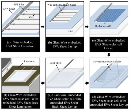
Figure 1.
Wire-embedded EVA sheet module process flow.
3. Results
It is essential to design the structure of the module before fabricating the wire-embedded EVA sheet module using the cell/module integrated process. Variables such as the number and spacing of wires interconnected with the finger electrode of the busbarless cell serve as important factors in determining the output of the module. In this study, the front electrode of the wire-embedded EVA sheet module was designed using various simulations such as Griddler 2.5 and MathCAD, and the influence of various variables such as the number of wires and wire diameters on the module power was analyzed. Cell parameters were applied based on a PERC-structured c-Si solar cell. For the parameters of the simulation, the size of the wafer was 156.75 × 156.75 mm2, the thickness of the wafer after texturing was approximately 170 µm, and the sheet resistance after the formation of the emitter was approximately 120 ohm/sq. At this time, the finger line width of the front electrode was fixed at 30 µm, and the number of fingers was set to 90. The optimum line width and efficiency values were derived based on the number of busbars in the front electrode. Figure 2 compares the measured values and the simulated values of module characteristics and the efficiency value based on the number of busbars with a line width of 0.26 mm. The efficiency increased as the number of busbars increased and decreased when the number of busbars was 38. As the number of busbars increases, the shading loss increases owing to the busbar area, which leads to optical loss, resulting in a decrease in efficiency. The module for this analysis was manufactured using a low-melting-point solder-coated wire with a line width of 0.26 mm, and the module was manufactured using one solar cell. The 1 × 1 unit module was manufactured based on the number of wires of 6, 12, 18, and 24 wires; a difference occurred between the simulation value and the actual efficiency measurement value. A wire-type busbar was used for contact with the finger line when a module was manufactured using a busbarless cell. Accordingly, the contact area and losses were different from those of the conventional busbar-type electrode. When a wire is applied, light reflection occurs on the curved surface of the wire, reducing the effective light-transmitting area of the busbar, which leads to a reduction in shading loss, which is a light loss owing to the busbar. It is necessary to perform a simulation of the front electrode based on the changed measurement conditions. The above simulation result using Griddler 2.5 is the value derived by setting the effective shading area of the busbar to a value of 100%. For a wire, part of the light is incident on the surface of the solar cell owing to the curved surface, and another part of the light is reflected; further, the reflected light is directly incident on the surface. Another part of the reflected light after encapsulation is reflected at the interface between the module glass and air and is then incident on the surface of the solar cell. Accordingly, the contact area between the finger line and wire is different because of the curved surface of the wire shape. The difference between the simulated and actual measured values occurred because the effective light transmission area ratio was different. The simulation program should derive the result by considering the contact area between the wires and the finger line.
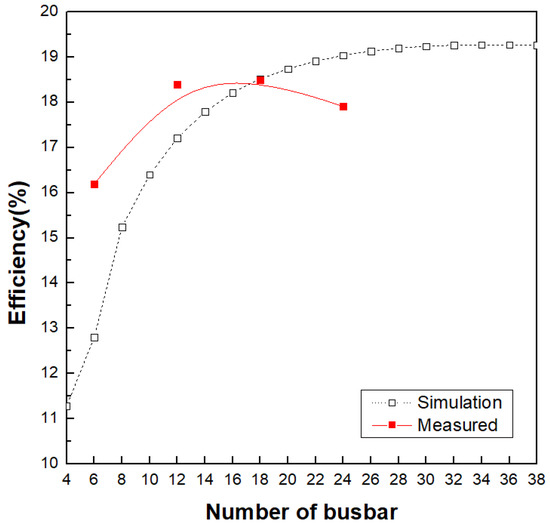
Figure 2.
Simulated values and measured values based on the number of busbars for c-Si solar cell.
Figure 3 shows the schematic of the conventional rectangle-type busbar and wires. Based on literature research [21], it was confirmed that the effective shading area was observed differently by the light incident on the wire. For a wire, the incident light is directly reflected on the cell surface, and the effective shading area is reduced to approximately 70% of the actual area. In area b, the incident light from the wire is reflected on the module glass, when the refractive index of the glass used in the module is 1.5. The effective shading area decreases to approximately 35%. In c, the light reflected from the round wire is reflected back to the module glass; however, the incident angle is larger than the total reflection angle, and therefore the light is divided into reflected and transmitted parts. Accordingly, the shading area of the wire is reduced, and incident light is vertically reflected by the wire, which is re-incident to the wafer surface. Contrastingly, incident light on the rectangular-shaped conventional busbar is less re-incident to the wafer surface. To measure the contact area between the wire and the finger electrode, a cross-sectional scanning electron microscope (SEM) image of the wire and the finger electrode was performed, as shown in Figure 4. The contact area between the wire and finger electrode was reduced by 70% of the wire diameter.
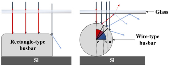
Figure 3.
Schematic of the conventional rectangle-type busbar and the wire.
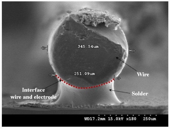
Figure 4.
Cross-section of the SEM image between wire and finger electrode.
The diameter and number of wires should consider the shading loss and the resistance loss simultaneously, and the diameter and number of wires that can minimize both factors should be selected. Because the module manufacturing based on the simulation results can proceed without significantly deviating from the range of the experimental conditions, the wire diameter according to the number of wires was derived using simulation as in MathCAD, and the design of the optimal wire electrode for actual module fabrication was performed. To design a simulation program, an approach to theoretical equations for solar cell parameters is required. Figure 5 shows the basic structure of a solar cell [22].
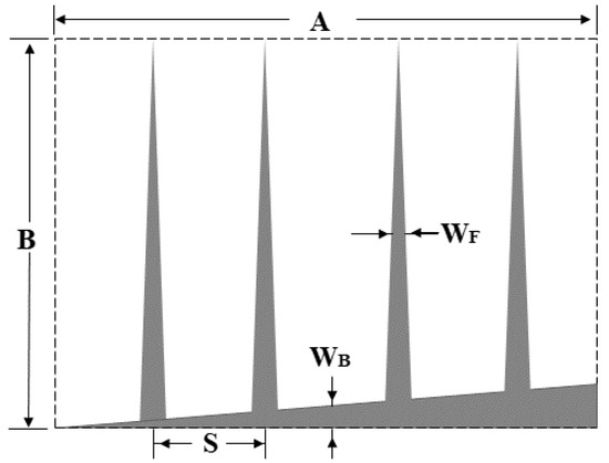
Figure 5.
Basic structure of a solar cell.
When the thickness of the electrode changes in the solar cell, the loss value of the electrode also changes. In the solar cell, the loss owing to the resistance of the electrode ( and the loss owing to the reduction of the light-emitting area by the electrode ( occur in the solar cell. The two losses owing to the electrodes are expressed as [22].
Here, and are the sheet resistances of the fingers and busbars, respectively; and are the thicknesses of the fingers and busbars, respectively; A and B are the lengths of each side of the solar cell unit structure, and S is the finger spacing. m is equal to 4 when the electrode shape is a tapered shape and 3 when the electrode shape is a square shape with a uniform width. As shown in the above equation, as the thickness of the busbar increases, the loss owing to resistance decreases, although the lighting area decreases, thereby increasing the shadow loss. Therefore, it is essential to establish an optimized busbar thickness that can minimize the sum of the two losses. The thickness of the busbar that can minimize the two losses is when the loss owing to resistance and shadow loss matches. In this study, the busbar of the busbarless cell solar cell was changed to a wire instead of the existing five busbars. Accordingly, the simulation program must be modified to accommodate such changes. After confirming the effective light transmission area ratio based on the busbar shape and the changed solar cell parameters, the simulation program was modified. Based on this simulation program, a graph shows the value of the optimum wire diameter versus the number of wires derived from a simulation program designed by applying the busbar shape as a wire. Figure 6 shows the value of the optimum wire diameter based on the number of wires derived from the simulation program. Wires with a diameter of 0.26 mm to 0.36 mm were used in this study, and the optimal number of wires was expected to be 10–12. Based on these simulation results, when the actual module was manufactured, the number of wires was set to a value between 6 and 24, which is in the range of 10–12.
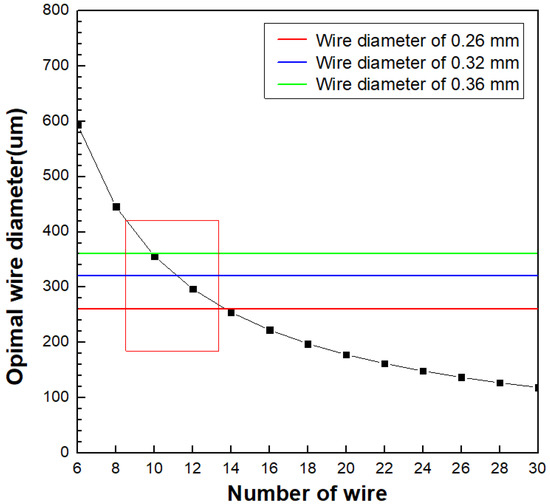
Figure 6.
Optimal wire diameter according to the number of wires.
There are busbar electrodes and finger line electrodes in front of the solar cell, and losses owing to these electrodes can be divided into shading loss and electrical resistance loss. To check the accuracy of the simulation results using MathCAD, an analysis of the output loss was conducted through a new program. The equation for designing a simulation program can be expressed as [23].
The shading loss is calculated by dividing the shading area of the electrode in the direction perpendicular to the incident light () by the area of the solar cell [24]. Here, is 0.1 W/cm2, which is the value of the solar energy density of AM1.5G, and is the ideal solar cell conversion efficiency value under the condition that there is no output loss owing to shading loss and resistance loss. This value can be calculated by applying pEff. through Suns-Voc measurements. represents the shading area corresponding to the front electrode, and represents the total area of the solar cell. The electrical resistance loss is calculated by the series resistance characteristics of the solar cell and is determined by the resistance value of each layer that affects the series resistance. The series resistance components generated in each layer are expressed as follows [23]:
The parameters of the equation are shown in detail in Table 1. The busbars included in the equation represent wires because the module was manufactured using wires instead of forming busbars on finger electrodes [23]. In the above equation, a is the finger length, and b is the half spacing. Meanwhile, A is the unit cell area, is the half-wire width, is the light-generated current, and is the incident light power density. The simulation was carried out based on the number of wires and diameter of the wires serving as busbars, and the simulation was conducted while changing each parameter.

Table 1.
Equation parameters.
Using the above simulation program, the total power loss based on the number of wires is shown in Figure 7, considering the shading loss and resistance loss. When the number of wires was 12, the lowest power loss was observed; further, the resistance loss was greater than the shading loss under the condition of fewer than 12 wires. The shading loss was greater than the resistance loss under the condition of 12 or more wires.
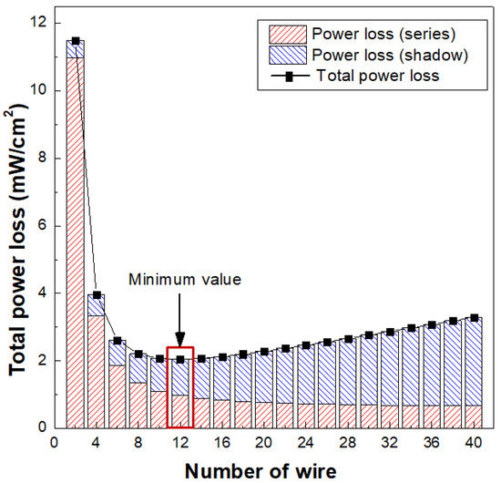
Figure 7.
The ratio of shading and resistance losses with respect to the number of wires.
Thus, the fill factor is expected to decrease significantly owing to resistance loss in modules of 12 lines or less, and short-circuit current characteristics are expected to decrease owing to shading loss in modules of 12 lines or more [24]. The difference between the simulated and actual measured values was compared when the actual module was manufactured based on the simulation results. The cause of the module power loss was analyzed. The wire-embedded EVA sheet module was fabricated by varying the number of wires to 6, 12, 18, and 24 and wire diameters of 0.26, 0.32, and 0.36 mm. Based on the simulation results, a module was fabricated using wires of three diameters. As shown in the simulation results, the number of wires was changed from 6 to 24 to include the number of wires between 10 and 12.
Figure 8 shows the characteristics of a module manufactured as a 1 × 1 unit module based on the wire diameter and number of wires. Under the conditions of three diameters, the rate of increase or decrease in efficiency of the number of wires showed a similar tendency, and the efficiency of the 1 × 1 unit module having a wire diameter of 0.36 mm and 12 wires showed the highest efficiency, at 20.28%. This is explained in Figure 9.
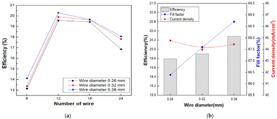
Figure 8.
Characteristics of a 1 × 1 unit module based on the number of wires (a) and the wire diameter (b).
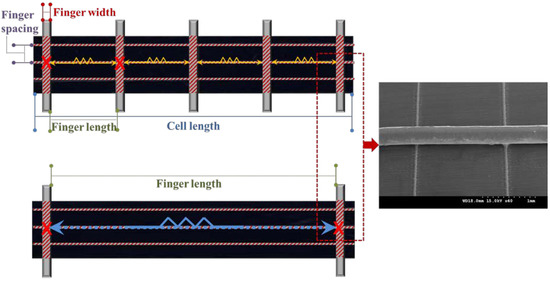
Figure 9.
Schematic of the cause of the increase or decrease in efficiency based on the number of wires.
The change in the short-circuit current was small, and the fill factor was greatly improved as the diameter increased. Although the optical loss increases as the wire diameter increases, the short-circuit current loss is small. As the diameter of the wire increases, the series resistance component significantly decreases, thereby improving the fill factor [25,26]. In addition, the efficiency of the module was also affected by the number of wires, and the highest efficiency was achieved when the number of wires was 12. The lowest efficiency was observed when the number of wires was 6, and the efficiency started to decrease as the number of wires increased to 12 or more. Figure 9 compares the results obtained when the number of wires is large and small. When the number of wires was large, the length of the finger electrode between the wires decreased. Accordingly, the resistance of the finger electrode decreased, although the optical loss was owing to the increased shading area. Conversely, as the number of wires decreased, the shading area decreases and optical loss decreased; however, the length of the finger electrode between the wires increased, indicating that the resistance of the finger electrode increased [27,28,29].
The 1 × 1 unit module was manufactured based on the diameter and number of wires, and the characteristics of the module were analyzed. A 2 × 2 unit module was manufactured by connecting the busbarless cells in series, and at this time, a comparative analysis was conducted based on the characteristic analysis result of the 1 × 1 unit module. Figure 10a shows the characteristics of a 2 × 2 unit module manufactured according to the number of wires. In the result of the 2 × 2 unit module characteristics, the highest efficiency was observed when the number of wires was 12, and the result was similar to the characteristics of the 1 × 1 unit module. The open-circuit voltage was similar to that of the wire; however, the short-circuit current decreased owing to shading loss. However, even if there is a loss owing to the short-circuit current, the overall efficiency increases owing to the increase in the fill factor. Figure 10b shows the characteristics of a module manufactured by changing the diameter of the wire after fixing the number of wires to 12. The efficiency of the module with a wire diameter of 0.36 mm showed the highest efficiency. This is similar to the characteristics of the 1 × 1 unit module. As the wire diameter increases, the contact resistivity with the finger electrode improves, resulting in a decrease in the series resistance. Consequently, the fill factor was improved. However, when compared to the 1 × 1 unit module, as the wire diameter increases, the value of the short-circuit current significantly decreases to a greater extent. This is because it is more affected by the short-circuit current value owing to shading loss.
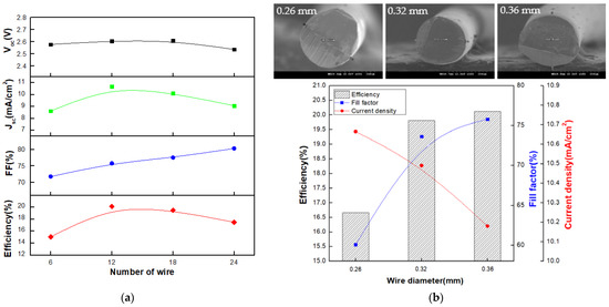
Figure 10.
Characteristics of a 2 × 2-unit module based on the number of wires (a) and wire diameter (b), and SEM im-ages of wires with diameter of 0.26 mm, 0.32 mm, 0.36 mm.
The cell/module characteristics of the tabbing module and the wire-embedded EVA sheet module were compared. Table 1 and Table 2 summarize the characteristics of the five-busbar tabbing module and wire-embedded EVA sheet module. Figure 11 shows the characteristic graph for the five-busbar tabbing module and wire-embedded EVA sheet module. For the expected power value of the 2 × 2-unit module, the maximum value of the module characteristics was calculated based on the sum of the Voc values of the four cells, the lowest Isc value, the average value of the fill factor, and the sum of Pmax. Table 2 lists the cell and module characteristics for the five-busbar tabbing modules, and Table 3 lists the cell and module characteristics for the wire-embedded EVA sheet module. For the FF (fill factor) value, the difference between the expected and measured values was confirmed. The reason for the decrease in the FF value in the measured value can also be explained by the increase in Rs. The FF can be expressed as a function of the series resistance and parallel resistance, and the series resistance can be changed by the front and rear electrodes. In particular, for the busbarless case, because the busbar, which is an important part of reducing the series resistance, is replaced or removed, the influence of the finger and the front structure on the total series resistance increases. The series resistance decreases from the expected value because of the influence of the resistivity of the wire and the contact resistance between the wire and the finger electrode, and the resistance of the ribbon to the string process of the module. The ratio of the difference between the calculated values and the measured value of power for the five-busbar tabbing module and wire-embedded EVA sheet module were 3.245% and 2.619%, respectively. As can be seen from Figure 11, it was confirmed that the power reduction characteristic of the wire-embedded EVA sheet module has a lower reduction rate of approximately 0.6% than the five-busbar tabbing module, and hence the loss when made from a cell to a module can be minimized. It was possible to manufacture a high-power module that sufficiently compensated for the disadvantages of the tabbing module.
Table 2.
Characteristics of the five-busbar tabbing module.
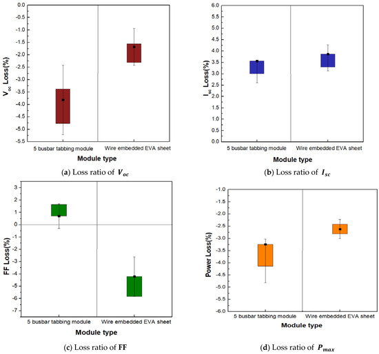
Figure 11.
Characteristics for five-busbar tabbing module and wire-embedded EVA sheet module.
Table 3.
Characteristics of a wire-embedded EVA sheet module.
To reduce the resistance of the finger electrode with a fine line width, the number of busbars must be increased, and an increase in the number of busbars in a solar cell reduces the length of the finger electrode between the busbars, thereby reducing the line resistance at the finger electrodes. The reduced finger line resistance reduces the resistance loss, and thus a relative gain in optical loss can be obtained along with the reduced loss ratio. As the number of busbars increases, the finger line width decreases, thereby reducing the shading area to minimize shadow loss and improve the optical characteristics. Based on the experimental results obtained in this study, it was confirmed that it is possible to manufacture a solar cell applicable to finger electrodes of fine patterns through a multi-busbar using a wire instead of a multi-busbar using a Ag paste. A module using wire can be expected to be an alternative modularization method to address limitations such as damage and deterioration of cell characteristics in the modularization process of thin wafers with the conventional tabbing method.
4. Conclusions
The module technology proposed in this paper is to manufacture a wire-embedded EVA sheet module with a cell/module integrated process. The wire-embedded EVA sheet module was fabricated by varying the number of wires to 6, 12, 18, and 24 with wire diameters of 0.26, 0.32, and 0.36 mm. The module with a wire diameter of 0.36 mm and 12 wires showed the highest efficiency, at 20.28%. The series resistance was significantly reduced, however, and the short-circuit current loss did not significantly decrease, despite the increased optical loss as the wire diameter increased. In addition, when the number of wires was increased, the resistance of the finger electrode decreased because the length of the finger electrode between the wire and the wire decreased; however, the optical loss increased because of the shading area. The cell/module characteristics of the tabbing module and the wire-embedded EVA sheet module were compared. The ratio of the difference between the calculated values and the measurement value for power of the five-busbar tabbing module and wire-embedded EVA sheet module were approximately 3.245% and 2.619%, respectively. The power of the wire-embedded EVA sheet module was confirmed to be better than that of five-busbar tabbing module. It was possible to manufacture a high-power module that sufficiently compensated for the disadvantages of the tabbing module. In addition, the wire-embedded EVA sheet module can be applied to thin wafers because it can remove heat and mechanical stress generated by the solar cell owing to the high-temperature tabbing process.
Author Contributions
J.E.P. was the main author and carried out the experiments and analyzed the data. W.S.C. reviewed and analyzed the data and formatting. D.L. conceived the ideas of the analyzed results. All authors have read and agreed to the published version of the manuscript.
Funding
This research was supported by Korea Electric Power Corporation (Grant number: R17XA05-1), the Korea Institute of Energy Technology Evaluation and Planning (KETEP) and the Ministry of Trade, Industry & Energy (MOTIE) of the Republic of Korea (No. 20193020010650).
Institutional Review Board Statement
Not applicable.
Informed Consent Statement
Not applicable.
Data Availability Statement
Not applicable.
Conflicts of Interest
The authors declare no conflict of interest.
References
- Xue, M.; Nazif, K.N.; Lyu, Z.; Jiang, J.; Lu, C.-Y.; Lee, N.; Zang, K.; Chen, Y.; Zheng, T.; Kamins, T.I.; et al. Free-Standing 2.7 μm thick ultrathin crystalline silicon solar cell with efficiency above 12.0%. Nano Energy 2020, 70, 104466. [Google Scholar] [CrossRef]
- Balaji, P.; Dauksher, W.J.; Bowden, S.G.; Augusto, A.J. Improving surface passivation on very thin substrates for high efficiency silicon heterojunction solar cells. Sol. Energy Mater. Sol. Cells 2020, 216, 110715. [Google Scholar] [CrossRef]
- Hasan, M.K.; Sasaki, K. Thermal deformation analysis of tabbed solar cells using solder alloy and conductive film. J. Mech. Sci. Technol. 2016, 30, 3085–3095. [Google Scholar] [CrossRef][Green Version]
- Lai, C.; Su, C.-H.; Lin, K. Analysis of the thermal stress and warpage induced by soldering in monocrystalline silicon cells. Appl. Therm. Eng. 2013, 55, 7–16. [Google Scholar] [CrossRef]
- Yoon, P.; Baek, T.; Chung, H.; Song, H.; Shin, S. Numerical simulation of bowing phenomenon in ultra-thin crystalline silicon solar cells. Sol. Energy 2014, 105, 705–714. [Google Scholar] [CrossRef]
- Fischer, M.; Hanwha, Q. CELL GmbH, Michael Woodhouse, The National Renewable Energy Laboratory, Susanne Herritsch, VDMA Photovoltaic Equipment, Jatta Trube. In International Technology Roadmap for Photovoltaic 11th; VDMA Photovoltaic Equipment, Lyoner Str.18; VDMA: Frankfurt am Main, Germany, 2020; p. 84. [Google Scholar]
- Ji, M.-K.; Park, S.M.; Kim, Y.R.; Kang, I.-C.; Kang, G.H. Photovoltaic systems’s cost saving technologies. The Magazine of Korean Solar Energy Society. Mag. Korean Sol. Energy Soc. 2015, 13, 11–17. [Google Scholar]
- Shin, D.-Y.; Lim, J.R.; Shin, W.-G.; Lee, C.-G.; Kang, G.-H. Layup-Only modulization for low-stress fabrication of a silicon solar module with 100 μm thin silicon solar cells. Sol. Energy Mater. Sol. Cells 2021, 221, 110903. [Google Scholar] [CrossRef]
- Kongwiriyaphaisan, A.; Tangwarodomnukun, V. Crack Reduction in Tabbing and Stringing Processes for Solar Cells. Key Eng. Mater. 2018, 777, 126–131. [Google Scholar] [CrossRef]
- Mittag, M.; Zech, T.; Wiese, M.; Blasi, D.; Ebert, M.; Wirth, H.; Cappelluti, F.; Gioannini, M.; Ghione, G.; Khalili, A. Cell-to-Module (CTM) Analysis for Photovoltaic Modules with Shingled Solar Cells. IEEE 2017, 2, 1531–1536. [Google Scholar]
- Papet, P.; Andreetta, L.; Lachenal, D.; Wahli, G.; Meixenberger, J.; Legradic, B.; Frammelsberger, W.; Bätzner, D.; Strahm, B.; Yao, Y.; et al. New cell metallization patterns for heterojunction solar cells interconnected by the Smart Wire Connection Technology. Energy Procedia. 2015, 67, 203–209. [Google Scholar] [CrossRef]
- Walter, J.; Tranitz, M.; Volk, M.; Ebert, C.; Eitner, U. Multi-Wire Interconnection of Busbar-free Solar Cells. Energy Procedia 2014, 55, 380–388. [Google Scholar] [CrossRef]
- Faes, A.; Lachowicz, A.; Bettinelli, A.; Ribeyron, P.; Lerat, J.; Munoz, D.; Geissbühler, J.; Li, H.; Ballif, C.; Despeisse, M. Metallization and interconnection for high-efficiency bifacial silicon heterojunction solar cells and modules. Met. Interconnect. 2018, 41, 65–76. [Google Scholar]
- Shravan, K. Chunduri, Michael Schmela. Market Survey Cell Interconnection Equipment 2017; TaiyangNews UG (haftungsbeschraenkt): Munich, Germany, 2017; pp. 1–40. [Google Scholar]
- Muehleisen, W.; Neumaier, L.; Hirschl, C.; Maier, T.; Schwark, M.; Seufzer, S.; Battistutti, R.; Pedevilla, M.; Scheurer, J.; Lorenz, R. Comparison of output power for solar cells with standard and structured ribbons. EPJ Photovolt. 2016, 7, 70701. [Google Scholar] [CrossRef]
- Söderströma, T.; Papetb, P.; Yao, Y.; Ufheilc, J. Smartwire Connection Technology. In Proceedings of the 28th EU-PVSEC, Paris, France, 30 September–4 October 2013; pp. 495–499. [Google Scholar]
- Silveira, A.; Barbin, S.E.; Kretly, L.C. Using TDR-Time Domain Reflectometry Measurements to Compare Ribbon Busbar versus Wire Busbar Connections in Polycrystalline Solar Cells: The Signature Approach. In Proceedings of the 2018 IEEE-APS Topical Conference on Antennas and Propagation in Wireless Communications, Cartagena, Colombia, 10–14 September 2018; pp. 954–956. [Google Scholar]
- Faes, A.; Despeisse, M.; Levrat, J.; Champliaud, J.; Badel, N.; Kiaee, M.; Soderstrom, T.; Yao, Y.; Grischke, R.; Gragert, M.; et al. SmartWire solar cell interconnection technology. Met. Workshop SmartWire CSEM 2014, 777, 126–131. [Google Scholar]
- Schulte-Huxel, H.; Blankemeyer, S.; Morlier, A.; Brendel, R.; Köntges, M. Interconnect-Shingling: Maximizing the active module area with conventional module processes. Sol. Energy Mater. Sol. Cells 2019, 200, 109991. [Google Scholar] [CrossRef]
- Yao, Y.; Papet, P.; Hermans, J.; Soderstrom, T.; Mehlich, H.; König, M.; Waltinger, A.; Habermann, D.; Richter, A. Module integration of solar cells with diverse metallization schemes enabled by SmartWire Connection Technology. In Proceedings of the 2015 IEEE 42nd Photovoltaic Specialist Conference (PVSC), New Orleans, LA, USA, 14–19 June 2015; pp. 258–262. [Google Scholar]
- Braun, S.; Micard, G.; Hahn, G. Solar Cell Improvement by using a Multi Busbar Design as Front Electrode. Energy Procedia 2012, 27, 227–233. [Google Scholar] [CrossRef]
- Green, M.A. Solar Cells: Operating Principles, Technology and System Applications; University of New South Wales: Sydney, NS, Australia, 1986; p. 274. [Google Scholar]
- Meier, D.L.; Schroder, D.K. Contact resistance: Its measurement and relative importance to power loss in a solar cell. IEEE Trans. Electron Devices 1984, 31, 647–653. [Google Scholar] [CrossRef]
- Stuckings, M.F.; Blakers, A.W. A study of shading and resistive loss from the fingers of encapsulated solar cells. Sol. Energy Mater. Sol. Cells 1999, 59, 233–242. [Google Scholar] [CrossRef]
- Nicolai, M.; Zanuccoli, M.; Magnone, P.; Galiazzo, M.; Tonini, D.; Bertazzo, M.; Sangiorgi, E.; Fiegna, C. Simulation Study of Multi-wire front Contact Grids for Silicon Solar Cells. Energy Procedia 2015, 77, 129–138. [Google Scholar] [CrossRef]
- Chen, N.; Chowdury, A.; Ahmad, E.; Unsur, V.; Ebong, A. Assessing the impact of multi-busbars on metallization cost and efficiency of solar cells with digital inkjet-printed gridlines. In Proceedings of the 2013 High Capacity Optical Networks and Emerging/Enabling Technologies, Magosa, Cyprus, 11–13 December 2013; Volume 8, pp. 60–65. [Google Scholar]
- Schneider, A.; Rubin, L.; Rubin, G. Solar Cell Efficiency Improvement by New Metallization Techniques—the Day4 Electrode Concept. In Proceedings of the 2006 IEEE 4th World Conference on Photovoltaic Energy Conference, Waikoloa, HI, USA, 7–12 May 2006; Volume 1, pp. 1095–1098. [Google Scholar]
- Braun, S.; Nissler, R.; Ebert, C.; Habermann, D.; Hahn, G. High Efficiency Multi-busbar Solar Cells and Modules. IEEE J. Photovolt. 2014, 4, 148–153. [Google Scholar] [CrossRef]
- Hsiao, P.-C.; Shen, X.; Wang, Z.; Song, N.; Li, Y.; Ouyang, Z.; Zhu, C.; Lv, J.; Shen, C.; Chen, C.; et al. Balanced contact method: Reduction of thermomechanical stress in silicon solar cells induced by interconnection. Sol. Energy Mater. Sol. Cells 2020, 215, 110667. [Google Scholar] [CrossRef]
Publisher’s Note: MDPI stays neutral with regard to jurisdictional claims in published maps and institutional affiliations. |
© 2021 by the authors. Licensee MDPI, Basel, Switzerland. This article is an open access article distributed under the terms and conditions of the Creative Commons Attribution (CC BY) license (https://creativecommons.org/licenses/by/4.0/).