Article

A Magnetic Field Camera for Real-Time Subsurface Imaging Applications

by
Andriyan Bayu Suksmono
1,*,
Donny Danudirdjo
1,*,
Antonius Darma Setiawan
2,
Dien Rahmawati
2 and
Rizki Putra Prastio
3
1
School of Electrical Engineering and Informatics, Institut Teknologi Bandung, Bandung 40132, Indonesia
2
School of Electrical Engineering, Telkom University, Bandung 40257, Indonesia
3
Faculty of Advanced Technology and Multidiscipline, Universitas Airlangga, Surabaya 60115, Indonesia
*
Authors to whom correspondence should be addressed.
Appl. Sci. 2021, 11(8), 3302; https://doi.org/10.3390/app11083302
Submission received: 26 February 2021 / Revised: 19 March 2021 / Accepted: 1 April 2021 / Published: 7 April 2021
(This article belongs to the Special Issue Magnetometers: Development and Application for the Last Decade)

Abstract

:

Featured Application

The proposed device can be used to find underground utilities that have ferromagnetic properties and subsurface power-line cable carrying electrical current.

Abstract

We have constructed an imaging device that is capable of showing the spatio-temporal distribution of magnetic flux density in real-time. The device employs a set of AMR (anisotropic magneto-resistance) three-axis magnetometers, which are arranged into a two-dimensional sensor array. All of the magnetic field values measured by the array are collected by a microcontroller, which pre-processes and sends the data to a PDU (processing and display unit) implemented on a smartphone/tablet or a computer. The interpolation algorithm and display software in the PDU present the field as a high-resolution video; thus, the device works as a magnetic field camera. In the experiments, we employ the camera to map the field distribution of the distorted ambient magnetic field caused by a hidden object. The obtained image of field shows both the position and shape of the object. We also demonstrate the capability of the device to image a loaded power-line cable carrying a 50 Hz alternating current.

1. Introduction

A camera is an image-capturing device. Early cameras used a chemical substance to record an image of an object. In principle, light rays reflected by an object are collected by a lens or a pinhole to form a small planar image, which falls on a negative film that contains a layer of photo-sensitive chemicals. In the photographic development process, the negative film is converted into a positive one on paper. Modern cameras record images digitally. The object image that has been projected onto a recording area is measured by a light-sensitive sensor array. The voltage values from the array are then digitized so that an array of numbers representing the image of the object can be stored in a digital format or displayed on a screen. Specialized cameras are usually named after the type of waves they capture, such as infra-red, X-ray or hyper-spectral cameras.
A distinctive feature of a camera is that all picture elements of the object image (or sequences of images/video) are captured simultaneously, instead of element-by-element or pixel-by-pixel. In the latter case, the device is usually called a scanner. A digital camera can also display the captured image instantly. Considering these features, in this paper, we refer to the generic name “camera” as a device that capable to capture and display a distribution of physical quantity of an object instantly. For optical cameras, the physical quantity is the reflectivity or physical response of the object from impinging lights (including the colors).
In [1], we constructed a magnetic field imaging system utilizing the built-in magnetometer of a smartphone. To obtain an image that represents the distribution of the magnetic flux density caused by an ambient magnetic field, such as the Earth’s magnetic field [2], one has to scan an imaging area and then execute a reconstruction algorithm to obtain all field values of the area. Therefore, this device is categorized as a scanner, which is referred to as a B-Scanner, where “B” refers to the notation of magnetic flux density, which is normally denoted by B . Magnetic field scanners have also been employed in geomagnetic surveys [3] and industrial testing [4]. Micro-circuitry faults of an IC (integrated circuit) can also be detected by a magnetic field scanner [5]. A close relative to magnetic imaging is eddy-current imaging, which has also been investigated actively by researchers [6,7,8,9,10]. In the biomedical area, extremely sensitive SQUID (superconducting quantum interference device)-based magnetometers have been used to detect and image brain activities in magnetoencephalography research [11,12].
In magnetic field surveys, one typically uses a highly sensitive sensor solely designed for research purposes [3]. Magnetic field sensors are currently easily found at low prices. These sensors make use of giant magneto-resistance (GMR) [13,14,15] or anisotropic magneto-resistance (AMR) phenomena, which refer to the change in resistance of a material due to the impact of a magnetic field. In contrast to conventional sensors such as proton magnetometers, GMR/AMR-based devices can be implemented as compact and low-cost IC sensors. Most mobile phones today include a built-in GMR/AMR magnetometer as one of their standard features.
This paper describes the design and realization of a magnetic field camera, or the B-Camera. The proposed B-Camera has the capability to capture and display the magnetic field distribution of a region instantly thanks to an array of magnetometers that simultaneously measures the field values on a regular grid of the area. Then, a reconstruction algorithm interpolates all of the values within the observed area and displays the result on a screen. We use a similar reconstruction and display subsystems as in the B-Scanner; i.e., data collected by the sensor-array are send to a PDU (processing and display unit), which can be implemented on smartphones, tablets or computers through a USB or a Bluetooth port.
The rest of the paper is organized as follows. In Section 2, we briefly describe the principle of the proposed B-Camera. The following Section 3 describes the experiments, including the arrangement, reconstruction of images and analysis of the results. Section 4 summarizes and concludes the paper.

2. Materials and Methods

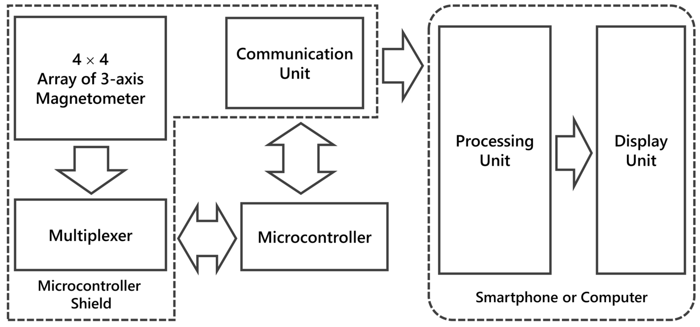
2.1. B-Camera: A Magnetic Field Camera

Human eyes cannot sense the presence of a magnetic field. To “see” the magnetic field, one can use iron powder. By pouring the powder onto a sheet of paper which is placed on top of a magnet, we obtain a picture of the magnetic field lines. The density of the field is indicated by the density of the lines. More accurate measurement requires the use of a magnetometer, which is usually moved around to scan an area while the field values are recorded. The field distribution can be derived by interpolating to locations within a surveyed area for which the values are unknown. For an instantaneous display of the field—as required in a camera—an array of magnetometers is necessary. In [16], a magnetic camera made of Hall-effect sensors has been proposed where the magnetic field strengths of observed objects are captured and displayed as a three-dimensional surface map.
Additionally, we also cannot perform focusing for a magnetic field, as is normally done in an optical camera by using a lens. Therefore, the field is sensed directly at the corresponding position by a magnetometer. The B-scanner in [1] operates using predefined grids over an observed area and measures the field at the center of each grid. Dividing the area into grid points is equivalent to the discretization of the space, whereas the magnetometer of a smartphone in the B-Scanner also gives discretized values of the magnetic field. The simultaneous observation of the field values on the area can be obtained by placing a number of sensors at the centers of the grids, yielding an array of magnetometers. At this point, there is a close similarity between the B-Camera and an optical camera.

2.2. Construction of the B-Camera

In principle, the B-Camera works in a similar way to the magnetic field scanner, unless the sensor positions are fixed at regular grid points/arrays. The block diagram displayed in Figure 1 shows the basic construction of the B-Camera.

2.2.1. Sensor Array and Multiplexer

The sensor array performs the spatial sampling of the magnetic field on an area, which is achieved by arranging the magnetometers into a two-dimensional array. The minimum spatial sampling size, or the size of a sampling grid, is related to the dimension of the sensor. Since the present implementation used an altered version of an HMC5883L magnetometer chip, we set the grid cell size to be 2 cm . The sensors were arranged into a 4 × 4 array, so that the total size of the sensed area was 8 × 8 cm 2 .
The HMC5883L sensor can measure a magnetic field up to 8 gauss (1 gauss = 10 4 tesla) in three axes. The chip employs the I2C (IC-to-IC Communication) protocol to communicate with other devices, which in this case was a microcontroller. Since all of the sensors had an identical fixed address, we employed a 1-to-16 multiplexer to access the field values of each sensor, which were controlled by four digital channels of the microcontroller. Thus, the measured field values could be read sequentially by the microcontroller from each sensor’s data registers.
The sensors were calibrated according to the self-test protocol given in the chip datasheet. An internal current source inside the IC generated a direct current that created ±1.1 gauss of artificial magnetic field bias on the sensors. By measuring these measured fields, one can test the sensor functionality and estimate its sensitivity for each axis. We excluded all sensors with more than 15% error compared to the expected readouts and adjusted all successive measurements based on the estimated sensitivity. Although this is not the best way to calibrate magnetic sensors, this setup was very useful to prevent us from obtaining poor-quality sensors that gave extremely incorrect data during experiments.

2.2.2. Microcontroller Unit

The main tasks of the microcontroller unit are to read the sensors, perform basic processing and to send the result to the PDU. We employed an Arduino microcontroller because of its availability, affordability and its openness. We read the data using the four digital channels of the microcontroller and translated the integer (scaled) field values into re-scaled proper values in gauss units. The results were then sent to the PDU by using a USB port, if the PDU was implemented on a computer, or by using a Bluetooth channel for the smartphone-based PDU.

2.2.3. Communication Unit

Either the USB or Bluetooth port can be used for communication between the sensor array and the processing unit. When mobility is prioritized, we can use a Bluetooth breakout such as the HC-06. The array data include the ID of each sensor, the three components of measured magnetic fields { B x , B y , B z } and a flag to indicate the end of a scan, so that the PDU can immediately process the data and display the image when all of the data in the array have been received.

2.2.4. PDU (Processing and Display Unit)

The PDU can be implemented on either a computer or a smartphone/tablet. Present-day smartphones, despite their affordability, have a sufficient computing power and display resolution to be used for this purpose. The main task of the computing part is to interpolate the two-dimensional magnetic field values into a larger size. We implemented two interpolation algorithms in our device; i.e., bilinear and bicubic [1,17]. These were coded in Java using Android Studio for the smartphone-based PDU and by using Matlab and Python for the computer-based PDU.
The bilinear method requires four known values obtained by measurements to estimate a field value at a particular point. Based on these known values, the values for desired positions are derived by using linear interpolation. The drawback of the bilinear method is that when the sampling points are sparsely distributed, the constructed field cannot be smoothly interpolated. To obtain a better result, we can use the bicubic method, which uses 16 neighboring values to estimate unknown values. The interpolation is done by a nonlinear function; therefore, a smoother result can be obtained.
The display unit shows the magnetic field distribution for each component and the total magnitude. For a given measured field at a discrete point ( m , n ) within the surveyed area, where m and n indicate the row and column number, respectively, the vector of magnetic field is given by
B ( m , n ) = B x ( m , n ) i ^ + B y ( m , n ) j ^ + B z ( m , n ) k ^
where i ^ , j ^ , k ^ are the unit vectors to the direction of x, y and z, respectively. The magnitude of the magnetic flux density is given by
| B ( m , n ) | = B x 2 ( m , n ) + B y 2 ( m , n ) + B z 2 ( m , n )
Each of the components { B x , B y , B z } and the magnitude | B | are displayed separately by the PDU system. The observation of directional field components is hardly possible in other imaging modalities such as optical imaging, ultrasound and non-polarimetric radar. This enriches the features, which can increase the recognition capability of the system.

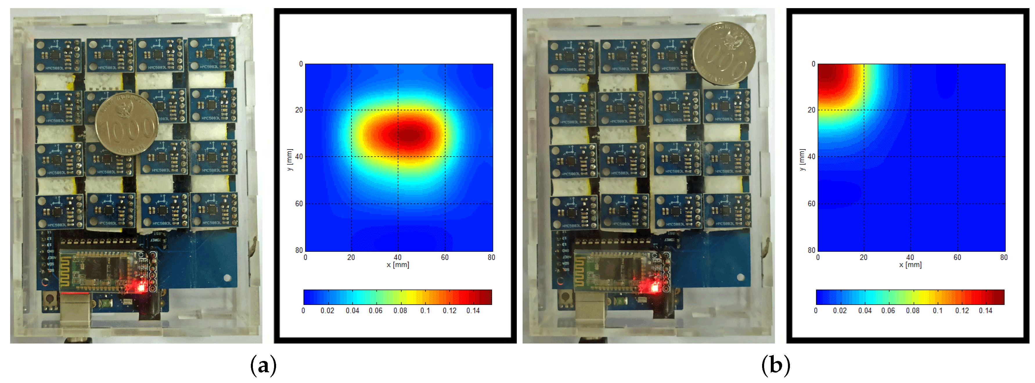
2.3. B-Camera with Larger Sensor Array

In order to test the scalability as well as to facilitate large-area observation, we constructed a system with a larger array consisting of 320 sensors in 5 × 4 subarrays. Figure 2 shows the block diagram of the system. The subarray consisted of 16 sensors connected via a 1-to-16 multiplexer to one slave microcontroller. Slave microcontrollers were connected to the master microcontroller via an SPI (Serial Peripheral Interface) bus. This allowed faster communication between those microcontrollers without the need for multiplexing. One operation cycle started with the master microcontroller giving orders to all slave microcontrollers to measure the field. Each slave microcontroller instructed the 16 sensors to start the measurement, wait before all the data were ready, collect the measured field data and send them to a master microcontroller. Lastly, the master microcontrollers sent the data via a communication unit to the computer-based PDU.
This cascade configuration allowed all slave microcontrollers to operate simultaneously in parallel. For the 20 subarrays, the time difference between the first and the last measurements (in one subarray) was measured at 4.6 ± 1.2 ms. This was due to the time required for the multiplexer to select and pass the data from the 16 sensors. The maximum time difference among the 320 sensors was 4.98 ms, which occurred between the measurements at the first sensor (of the first subarray) and the last sensor (from the last subarray). Since these maximum time differences were still less than the sensor’s conversion time in single measurement mode, this showed the potential to incorporate more sensors in a scalable manner without losing too much speed.

3. Experiments and Analysis

3.1. Imaging a Coin with a Smartphone-Based PDU

In this experiment, we used the B-Camera with a smartphone-based PDU. The object was a nickel coin (Rp.1000), which possesses a ferromagnetic property. In the first experiment, the coin was located at the center of the array, as shown in the left part of Figure 3a. The magnitude field distribution expressed in Equation (2) was displayed on a smartphone screen, as shown in the right part of Figure 3a. The colors represent the field density in gauss (G), whose values are indicated in the color bar. The image showed the circular distribution of the field, which was strong at the center of the array. This image was consistent with the position of the object.
In the second experiment, the coin was located in the corner of the array. It should be noted that in normal usage, the array looks downward; therefore, the left–right positions are exchanged. The left part of Figure 3b shows the position of the object in the array, whereas the right part shows the field distribution. This figure shows that the image of the object was as expected, indicating that the device worked properly.

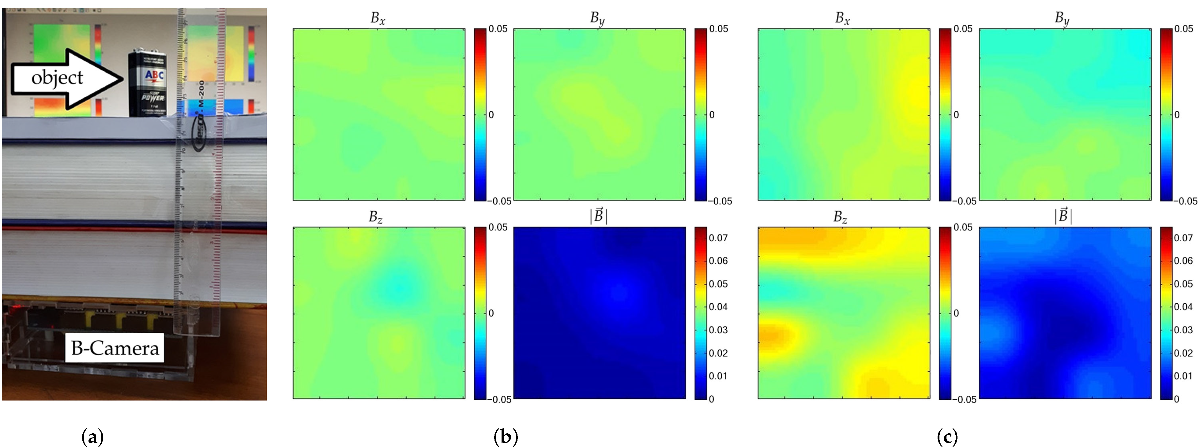
3.2. Observation of a Hidden Object

In this experiment, an object (a 9 V dry-cell battery) was located on a top of a book stack. We used a B-Camera with a computer-based PDU. The microcontroller (Arduino) was connected to the USB port of the computer where a PDU program was running. We easily obtained a better color contrast by adjusting the range of the colormap, which enhanced the display of the magnetic field distribution. The purpose of this experiment was to show that a hidden object separated by a thick wall could be detected (and imaged) by the B-Camera.
Figure 4 shows (a) the experiment setting (test-range), (b) the field distribution before an object was placed in the array and (c) the field distribution after the object was placed on top of a book stack. The ruler in Figure 4a indicates that the distance between the sensor array to the object was around 12 cm. By comparing the field distribution without the object in Figure 4a with the one with an object shown in Figure 4b, we can see that the field changed and therefore the B-camera was capable of sensing the field of an object located behind a non-magnetic thick wall.
Experiments using large sensor arrays are shown in Figure 5. First, we measured the flux density around a C-clamp made of cast iron that was placed 3 cm above the sensor array, separated by air. The maximum flux density around 0.3 G was measured near the thick parts of the clamp, which was located close to the sensors. The second experiment used an X-shaped lug wrench made of stainless steel. Although the wrench was placed on top of a 5 cm-thick stack of non-magnetic papers, the measured fields were greater than those found in the clamp experiment. The difference in field magnitude measured around the rods was due to the different lug nut sizes (from 19 to 23 mm) and their distance to the sensors. Figure 5 shows the measured flux density in a normalized vectorial format ( B x / | B | , B y / | B | ) superimposed on the magnitude | B | in gauss, shown in colors. Shorter arrows indicate that the fluxes were oriented more vertically (to/from the sensor array), which usually corresponded to a greater field magnitude due to nearby magnetic objects. The images show the capability of the device to provide rough information of the shape of both objects.

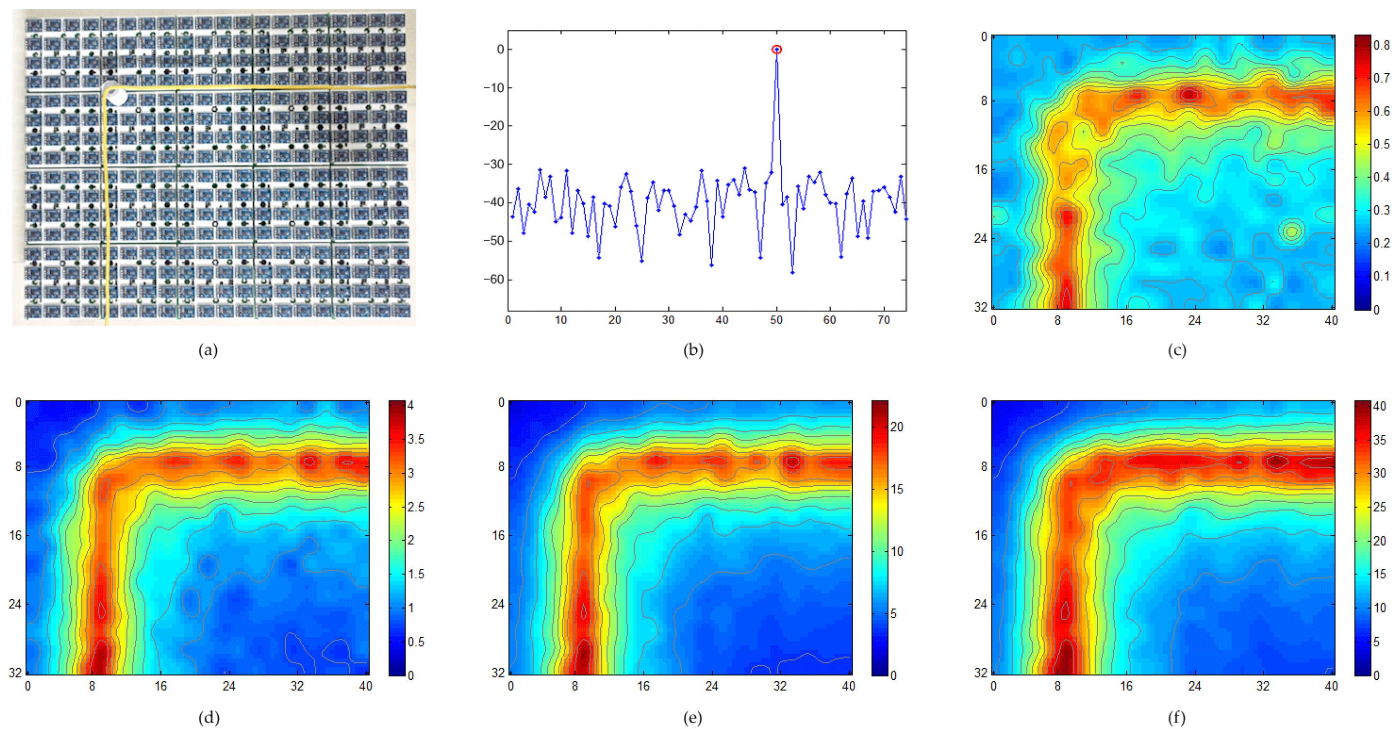
3.3. Imaging a Loaded Power-Line Cable

In this experiment, we measured the magnetic field induced by a current in a loaded 50 Hz power-line cable. We used a single-wire cable that was bent into an L-shape and placed around 3 cm above the large sensor array. The flux density around the cable was proportional to the current I and approximately inversely proportional to the distance between the wire and the sensor. Figure 6a shows the experiment setup. Since the array was planar, the field was stronger at points close to the cable and weaker at the top-left and bottom-right of the area.
The sampling rate of the magnetometer was set to 150 Sa/s for all field components. Figure 6b shows the spectrum of 1 s of measured B z data given by the sensor located below the cable’s bend point. The spectrum, estimated using a FFT (fast Fourier transform), showed a peak at 50 Hz. The frequency resolution was 1 Hz, which was due to the 1 s observation time. If necessary, one can increase the frequency resolution by using longer data measurements. It can be seen from the spectrum in Figure 6b that the measured peak frequency was slightly less than 50 Hz (which is common in 50 Hz power lines). In fact, if we used a 15 s measurement, the peak would be located at 49.917 Hz.
Figure 6c–f shows the norm of the three-directional magnitude of 50 Hz components of magnetic flux density at each sensor for four values of current; i.e., I rms = 12.6 mA, I rms = 68.3 mA, I rms = 355.5 mA and I rms = 1.037 A. The figures show that the measured field increased with the increasing current and that it was stronger near the cable and weaker at the two corners as expected.

4. Conclusions

This paper reports the construction of magnetic field camera using an array of digital magnetometers. As a proof-of-concept, we built a system using 4 × 4 sensor elements connected via a multiplexer to a processing unit and tested it to measure the magnetic field of ferromagnetic objects behind a surface. As we were convinced by the results, we built a larger 40 cm × 32 cm sensor array using 20 subarrays of 16 sensor elements in a mixed parallel-multiplexed manner. The camera was demonstrated to map the spatial distribution of magnetic flux density, which could be useful to detect hidden ferromagnetic objects and to readily display the distribution without the need for offline data storage/processing. Additionally, the high sampling rate of the sensors also allowed the camera to measure and map the distribution of a magnetic field near a loaded 50 Hz power-line cable.

Author Contributions

Conceptualization, A.B.S.; methodology, A.B.S.; software, A.B.S. and D.D.; validation, A.B.S. and D.D.; formal analysis, A.B.S.; investigation, A.B.S., D.D., D.R., and R.P.P.; resources, A.D.S., D.R., and R.P.P.; data curation, A.D.S., D.R., and R.P.P.; writing, original draft preparation, A.B.S.; writing, review and editing, A.B.S. and D.D.; visualization, A.B.S. and D.D.; supervision, A.B.S.; project administration, A.B.S. and D.D.; funding acquisition, A.B.S. All authors read and agreed to the published version of the manuscript.

Funding

This research was funded by ITB-Asahi Glass Foundation Research Grant 2018 and the ITB-P3MI Research Grant 2020.

Conflicts of Interest

The authors declare no conflict of interest.

References

  1. Suksmono, A.B.; Danudirdjo, D.; Setiawan, A.; Rahmawati, D. Magnetic subsurface imaging systems in a smartphone based on the built-in magnetometer. IEEE Trans. Magn. 2017, 53, 3200405. [Google Scholar] [CrossRef]
  2. Larmor, J. Possible rotational origin of magnetic fields of sun and earth. Electr. Rev. 1919, 85, 412. [Google Scholar]
  3. Mariita, N. The gravity method. In Proceedings of the Short Course II on Surface Exploration for Geothermal Resources (UNU-GTP and KenGen), Lake Naivasha, Kenya, 2–17 November 2007; pp. 1–9. [Google Scholar]
  4. Orozco, A.; Gaudestad, J.; Gagliolo, N.E.; Rowlett, C.; Wong, E.; Jeffers, A.; Cheng, B.; Wellstood, F.C.; Cawthorne, A.B.; Infante, F. 3D magnetic field imaging for non-destructive fault isolation. In Proceedings of the ISTFA 2013, San Jose, CA, USA, 3–7 November 2013; pp. 189–193. [Google Scholar]
  5. Knauss, L.A.; Woods, S.I.; Orozco, A. Current imaging using magnetic field sensors. Microelectron. Fail. Anal. Desk Ref. 2004, 5, 303–311. [Google Scholar]
  6. McCary, R.; Oliver, D.; Silverstein, K.; Young, J. Eddy current imaging. IEEE Trans. Magn. 1984, 20, 1986–1988. [Google Scholar] [CrossRef]
  7. Tsukada, K.; Kiwa, T.; Kawata, T.; Ishihara, Y. Low-frequency eddy current imaging using MR sensor detecting tangential magnetic field components for nondestructive evaluation. IEEE Trans. Magn. 2006, 42, 3315–3317. [Google Scholar] [CrossRef]
  8. Volk, M.; Whitlock, S.; Wolff, C.H.; Hall, B.V.; Sidorov, A.I. Scanning magnetoresistance microscopy of atom chips. Rev. Sci. Instrum. 2008, 79, 023702. [Google Scholar] [CrossRef] [PubMed]
  9. Joubert, P.Y.; Diraison, Y.L.; Xi, Z.; Vourc’h, E. Pulsed eddy current imaging device for non destructive evaluation applications. In Proceedings of the IEEE-SENSOR 2013, Baltimore, MD, USA, 3–6 November 2013. [Google Scholar]
  10. Bore, T.; Placko, D.; Joubert, P.-Y. Semi-analytical modeling of an eddy current imaging system for the characterization of defects in metallic structures. In Proceedings of the 2015 IEEE Sensors Applications Symposium (SAS), Zadar, Croatia, 13–15 April 2015. [Google Scholar]
  11. Cohen, D. Magnetoencephalography: Detection of the brain’s electrical activity with a superconducting magnetometer. Science 1972, 175, 664–666. [Google Scholar] [CrossRef] [PubMed]
  12. Hämäläinen, M.; Hari, R.; Ilmoniemi, R.J.; Knuutila, J.; Lounasmaa, O.V. Magnetoencephalography—Theory, instrumentation, and applications to noninvasive studies of the working human brain. Rev. Mod. Phys. 1993, 65, 413. [Google Scholar] [CrossRef] [Green Version]
  13. Baibich, M.N.; Broto, J.M.; Fert, A.; Dau, F.N.V.; Petroff, F.; Etienne, P.; Creuzet, G.; Friederich, A.; Chazelas, J. Giant Magnetoresistance of (001)Fe/(001)Cr Magnetic Superlattices. Phys. Rev. Lett. 1988, 61, 2472. [Google Scholar] [CrossRef] [PubMed] [Green Version]
  14. Binasch, G.; Grunberg, P.; Saurenbach, F.; Zinn, W. Enhanced magnetoresistance in layered magnetic structures with antiferromagnetic interlayer exchange. Phys. Rev. B 2004, 39, 4828. [Google Scholar] [CrossRef] [PubMed] [Green Version]
  15. Moodera, J.S.; Kinder, L.R.; Wong, T.M.; Meservey, R. Large Magnetoresistance at Room Temperature in Ferromagnetic Thin Film Tunnel Junctions. Phys. Rev. Lett. 1995, 16, 3273–3276. [Google Scholar] [CrossRef] [PubMed]
  16. Tuan, B.A.; de Souza-Daw, A.; Hoang, T.M.; Dzung, N.T. Magnetic camera for visualizing magnetic fields of home appliances. In Proceedings of the 2014 IEEE Fifth International Conference on Communications and Electronics (ICCE), Danang, Vietnam, 30 July–1 August 2014; pp. 370–375. [Google Scholar]
  17. Suksmono, A.B. Interpolation of PSF based on compressive sampling and its application in weak lensing survey. Mon. Not. R. Astron. Soc. 2014, 443, 919–926. [Google Scholar] [CrossRef]
Figure 1. A block diagram of the B-Camera showing its subsystems and their interactions. It consists of an array of magnetometers and a multiplexer (implemented as an Arduino shield), a microcontroller unit (Arduino), a communication unit (Bluetooth or USB port) and a processing and display unit (implemented in a smartphone or a computer).
Applsci 11 03302 g001
Figure 2. The system with a larger sensor array consisting of 320 sensors in 20 subarrays. Each subarray had 4 × 4 sensors, a multiplexer and a slave microcontroller connected to the master microcontroller via a Serial Peripheral Interface (SPI) bus. This configuration allowed faster data collection and simultaneous operation for all subarrays.
Applsci 11 03302 g002
Figure 3. Position of an object in the B-Camera’s array and corresponding magneto-photograph. The array was designed to be used downward; thus, the left–right position of the image has been inverted. The object was a Rp.1000 nickel coin: (a) positioned at the center of the the array, (b) located in the corner of the array. Images on at the right part of (a,b) show the consistency of the field distribution with their corresponding locations at the left part.
Applsci 11 03302 g003
Figure 4. Experiments to show the capability of the B-Camera to image a hidden object. (a) A dry-cell battery, the cover of which was made of iron, was located on top of a book stack to simulate a 12 cm wall hiding an object. (b) Magnetic field distribution with subtracted background without an object. (c) Field distribution after the object was put on top of the book stack. Color bar in (b) indicates magnetic flux density in gauss units. By comparing figure (b) to (c), we observe that the field distribution changed. This shows that the device was capable of detecting (and imaging) ferromagnetic objects hidden behind a thick non-magnetic wall.
Applsci 11 03302 g004
Figure 5. Experiments with a large array showed that the system could be used to roughly image more complex objects. Top: The experiment result with an iron clamp placed 3 cm from the sensors. Bottom: Experiment with an X-shaped stainless steel lug wrench hidden behind a 5 cm-thick stack of papers.
Applsci 11 03302 g005
Figure 6. Imaging a loaded 50 Hz power-line cable. (a) The experiment setup, where a yellow L-shaped current carrying cable was placed around 3 cm above the B-Camera. (b) The fast Fourier transform (FFT) spectrum, in dB, of 1 s of data captured at 150 Sa/s. (cf) Images depicting the magnitude of the 50 Hz component of the 1 s of data observed by each sensor for (c) I rms = 12.6 mA, (d) I rms = 68.3 mA, (e) I rms = 355.5 mA, and (f) I rms = 1.037 A. Note that the images use different color scales; the shown values are in milligauss.
Applsci 11 03302 g006
Publisher’s Note: MDPI stays neutral with regard to jurisdictional claims in published maps and institutional affiliations.

