1. Introduction
Among the displays currently in mass production, organic light-emitting diodes (OLED) are the only flexible devices which can be manufactured in various forms, unlike LCDs or other displays [
1,
2]. It is also being developed into stretchable and wearable form, so it looks to be very scalable [
3,
4,
5]. In particular, OLED has a fast response speed, high contrast ratio, lightness, and flexible characteristics, so its application product range is very wide, from small-sized devices through medium-sized devices such as notebooks and monitors to large-sized OLED TVs [
6,
7,
8]. Among these OLEDs, currently, quantum dot (QD)-OLED is now attracting considerable attention due to the high color gamut, wide viewing angle, and its many other advantages [
9,
10].
QD-OLED is a display made of OLED and semiconductor nanocrystals called quantum dots (QD) which produce pure monochromatic colors. In other words, the red QD and the green QD are stacked on a blue OLED that is used as an incident light source to express the desired colors of red and green by means of light conversion [
11]. Several studies on QD unit devices are in progress, although few studies have reported on how to proceed from the device or the process architecture to improve the overall color gamut [
12,
13].
Therefore, in this study, how to improve the color purity of QD-OLED was systematically reported in terms of device and process architecture. Firstly, in order to obtain high color gamut, which is known as one of the main advantages of QD-OLED, it is necessary to systematically investigate the influence of QD layer components, that is, QD density and QD layer thickness. In order to achieve this purpose, in particular, this paper was conducted to optimize the emission spectrum of green QD(G-QD) according to the optimal process architecture by modeling from the QD layer’s viewpoint and overall device optimization. Through this whole investigation, the optimal device structure of a green color with high color purity characteristics was found.
The SEmiconducting Thin Film Optics Simulation (SETFOS) tool was used for this optimal device modeling. This tool follows the Monte Carlo numerical analysis of carrier transport between organic semiconductor layers between two electrodes [
14]. Using this tool, the emission spectrum of high color purity was systematically analyzed, and the optimal structure of the QD-OLED layer structure with excellent color purity was developed.
2. Materials and Methods
2.1. Device Modeling of the OLED Multi-Layers
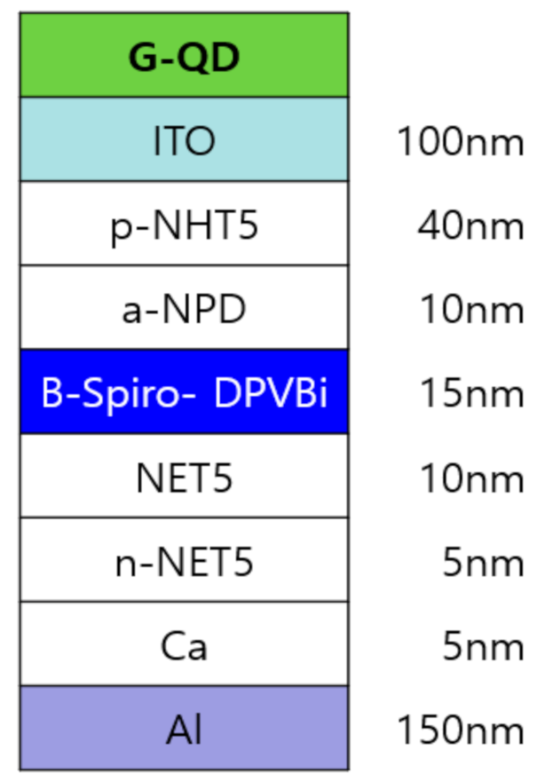
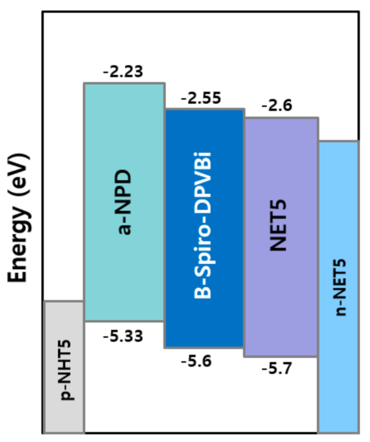
Figure 1 shows the material and thickness of each layer of the OLED structure with multiple layers investigated in the present study. In order to more effectively investigate the change in the emission spectrum according to the wavelength from a structural perspective, a structure in which a cathode is stacked at the bottom and an anode is stacked at the top was employed. A 150 nm-thick aluminum was used as cathode electrode material, and 5 nm-thick Ca was added between the n-electron transport layer (ETL) and aluminum layers to facilitate electron movement by improving the contact property with the n-ETL layer. For the n-doped electron-injecting layer (EIL), 40 nm of n-NET5 was applied, and 10 nm of NET5 was used as the ETL. In order to create an incident light in the blue wavelength band where absorption occurs most in the G-QD, blue OLED materials were stacked as the emitting layer. The blue, fluorescent layer was a 15 nm spiro-DPVBi (B-Spiro-DPVBi). A 100 nm transparent indium–tin oxide (ITO) rod was applied as the anode electrode. A 10 nm p-NHT5 was employed as a p-doped hole-injection layer, and a 10 nm a-NPD was used as the hole-transport layer. The energy level of the multi-layer OLED is shown in
Figure 2. The highest occupied molecular orbital (HOMO) levels of the a-NPD, blue, fluorescent layer, B-Spiro-DPVBi, and NET5 were −2.33, −2.55, and −5.6 eV, respectively, and the lowest unoccupied molecular orbital (LUMO) levels were −5.33, −5.6, and −5.7 eV, respectively.
First, the emission spectrum was investigated in the absence of a G-QD layer. After the device was optimized for the basic blue OLED unit, the effect of G-QD layers was investigated with stacked structure, as shown in
Figure 1. In this figure, the G-QD layer exists on top of the indium–tin oxide (ITO) layer. Specifically, a top emission structure in which the generated light is emitted toward the ITO was applied by placing the Al cathode at the bottom and the ITO anode at the top. Through this structure, it was possible to simulate the effect of blue incident light on the emission spectrum through the conversion effect after being absorbed into the QD layer.
The density and thickness were considered as variables of the G-QD layer. The concentration of G-QD used in the simulation was 1%, 5%, 10%, 20%, 30%, and 40%. At various concentrations, we tried to see the emission spectrum change according to the wavelength. In addition, after fixing the concentration at 10%, the emission spectrum change was observed while changing the G-QD thickness to 2 μm, 4 μm, 6 μm, 8 μm, and 10 μm in order to investigate the influence of the thickness.
2.2. Process Architecture Modeling of QD-OLED
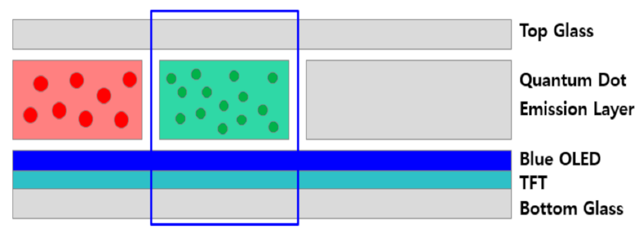
Figure 3 shows the schematic diagram of the QD-OLED process architecture considered for the design of this study. As mentioned in Chapter 2.1, in order to investigate the effect of emission spectrum of blue incident lights through G-QDs, G-QD layers were additionally stacked on top of the ITO for the OLED multi-layers, which is shown in
Figure 1. The thin film transistor is located under the blue OLED multi-layers, and the bottom glass is located as the base layer.
Additionally, as seen from the QD-OLED process architecture above in
Figure 3, it can be seen that the following parts must be considered in order to maximize the external quantum efficiency (EQE) when blue light is incident into QDs: the efficiency of the blue incident light into the QD layer (η
B), the efficiency of the blue light conversion through the QD (η
c), and the efficiency of light out-coupling to the air (η
out) [
15].
Therefore, it can be seen that to improve the overall external quantum efficiency, the efficiency of the incident blue light needs to be increased, as well as both efficiencies of light conversion (through QDs) and light out-coupling. In this paper, because we focus on the emission spectrum through QD layers, we would like to report this efficiency performance through further work.
3. Results and Discussion
3.1. Emission Spectrum with Different G-QD Densities
The emission spectrum according to the wavelength was first investigated using a 15 nm spiro-DPVBi, which is a fluorescent blue material.
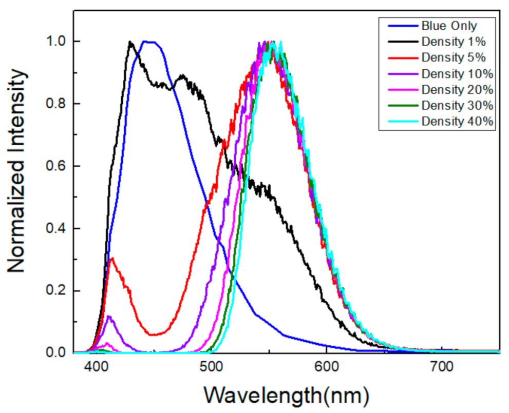
Figure 4 shows that the blue material’s emission spectrum analysis indicates the maximum peak in the 445 nm wavelength band. In addition, as a result of the blue color coordinated analysis using CIE1931 to investigate the color purity, we can observe that the blue color coordinate in the CIE1931 color space chromaticity diagram indicates that Bx is 0.15 and By is 0.12. Additionally, according to the wavelength, the emission spectrum was investigated while changing the QD volume density from 1% to 40%. From the results shown in
Figure 5, the thickness of the G-QD layer was fixed at 10 μm, a condition that minimizes light leakage in the blue wavelength band and obtains a sharp peak in the green wavelength band. As the blue OLED incident light passes through 1% of the G-QD density, most of the emission spectrum occurs only in the blue wavelength band and is only weakly observed in the green wavelength band. This result is thought to be due to the low G-QD density in the G-QD layer, so that blue incident light cannot be sufficiently scattered through G-QD, resulting in a low conversion rate to green color. It can be seen that when the G-QD density increases to 5%, the blue spectrum rapidly decreases, and the green spectrum increases. This result can be assumed to occur because the blue incident light is actively scattered through G-QD when the G-QD density is 5% or more. However, even in this condition, the full width at half maximum (FWHM) at a green wavelength is still large, at about 59.62 nm. When the G-QD density is more than 20%, the FWHM decreases rapidly in the green wavelength band, and sharper peaks are obtained. When G-QD is over 30%, blue light leakage in the blue wavelength band becomes very weak, the peak in the green wavelength band becomes very sharp, and the FWHM is reduced to 40.82 nm, showing a saturation behavior. Therefore, it can be seen that in order to minimize blue light leakage and obtain a sharp green peak with a narrow FWHM, the G-QD density should be at least 30%.
3.2. Emission Spectrum with Different G-QD Thicknesses
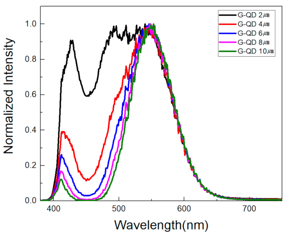
Figure 5 shows the emission spectrum according to the thickness of the G-QD layer when the G-QDs density in the layer is 10%. As shown in
Figure 5, when the thickness of the layer is 2 μm, the emission spectrum is strong in both the blue and green wavelength bands. This happens because the thickness is too thin; thus, the blue incident light cannot be adequately scattered in the layer. In other words, it can be seen that a large portion of the blue incident light passes through the layer and generates blue light leakage, and some of the light is scattered in this layer, contributing to the intensity of the green emission spectrum. When the thickness is increased to 4 μm, the emission spectrum in the blue wavelength band tends to decrease rapidly. However, the FWHM in the green region is 67.63 nm, which is still large, and the peak is broad. This tendency shows an improved behavior when the thickness increases to 6 μm or more and almost disappears at the 10 μm thickness, resulting in sharp peaks (FWHM 46.59 nm) in the green region. However, even at a thickness of 10 μm, an emission spectrum due to blue light leakage is still observed in the blue wavelength band. In other words, it would be difficult to completely block blue light leakage by simply increasing the thickness of the layer. Therefore, it seems necessary to supplement the device structure to increase the green color quality.
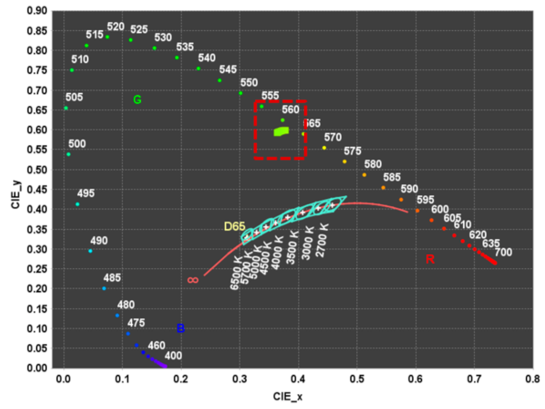
Figure 6 shows the CIE1931 color space chromaticity diagram when the thickness of the G-QD layer is 10 μm. As shown in
Figure 6, the color coordinates of Gx and Gy are 0.364 and 0.592, respectively. It shows a value that is less than the standard color coordinates, Gx 0.170 and Gy 0.797 for deep green in Rec. 2020 or BT2020 being used for ultra-high-definition television and a wide color gamut [
16,
17]. It can be seen that to increase the green color purity, the G-QD layer should not be used alone, but the color purity should be increased by reinforcing an additional layer above the G-QD layer.
3.3. New Device Architecture for Reduction in the Blue Light Leakage
As shown in
Section 3.1 and
Section 3.2, even if the density of G-QD is increased to 40% and the thickness of the G-QD layer is increased to 10μm it is difficult to completely block the leakage of blue light. In addition, the green color purity due to blue leakage is far below the deep green level of BT2020. Therefore, in order to completely block blue light leakage and improve green color purity, the existing process architecture has limitations, and an additionally supplemented structure must be considered.
In general, in the TFT-LCD process used in existing LED TVs, red, green, and blue color layers, which are called color filters, are stacked on the TFT pixels to express colors [
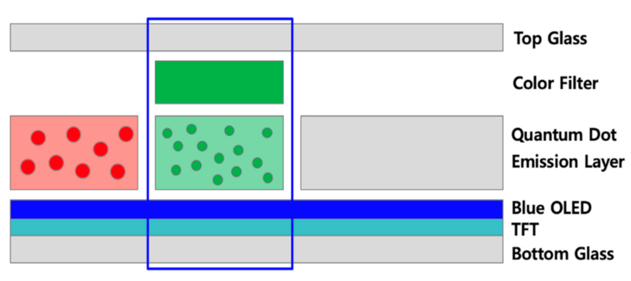
18]. Introducing such a similar structure to QD-OLED may improve color purity. Therefore, in this study, as shown in
Figure 7, we investigated whether the color purity increases by introducing a structure in which a new color layer is stacked on top of the QD layer.
3.4. Emission Spectrum of G-QD with Different G-CF Thicknesses
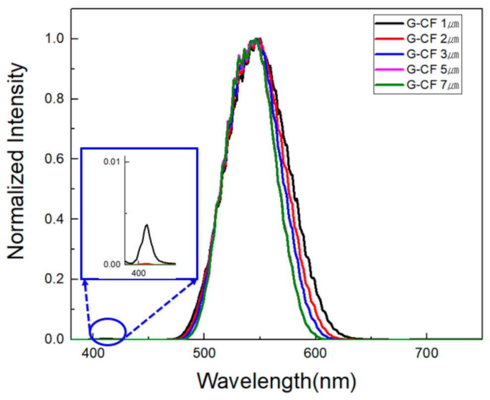
Figure 8 shows the emission spectrum according to the thickness of green color filter (G-CF) stacked on the G-QD layer. As shown in the enlarged picture in
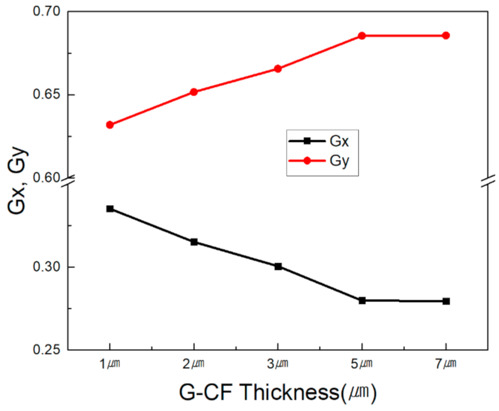
Figure 8, it can be seen that the blue light leakage in the blue wavelength region is minutely present when the G-CF thickness is 2 μm. However, when the G-CF thickness increases to 3 μm or more, it weakens gradually and is completely blocked from 5 μm. It can also be seen that the FWHM is gradually decreased and saturated from 5 μm. Therefore, it is determined from these results, that the thickness of the G-CF layer above the G-QD layer is needed to be about 5 μm to completely block blue light leakage and obtain a sharp peak in the green emission spectrum. This result can be seen in a graph of the influence of Gx and Gy color coordinates on the thickness of the G-CF layer above the G-QD layer in
Figure 9. As the G-CF thickness increases, Gx decreases and Gy increases. When the thickness of the G-CF layer is more than 5 μm, Gx and Gy are 0.280 and 0.686, respectively, showing saturation behavior. These Gx and Gy values are more improved than Gx 0.364 and Gy 0.592 obtained only with the G-QD layer, as shown in
Figure 6, and it can be seen that they are a little closer to the deep green of BT2020. In other words, the blue light leakage is well blocked when the G-CF thickness on the G-QD layer is more than 5 μm, and the purity of green color is improved as well. This also means that it is unnecessary to stack more than 5 μm of G-CF thickness to increase green color quality.
4. Conclusions
In this paper, through QD-OLED device modeling, the optimal structure for obtaining high green color purity was investigated. It was difficult to completely block light leakage in the blue wavelength band with only the G-QD layer. In other words, when the G-QD thickness is 10 μm, the G-QD density inside the G-QD layer should be filled with at least 30% to minimize the FWHM of the spectrum in the green wavelength band, although a minute light leakage in the blue wavelength band exists. In the structure in which G-CF was stacked over 5 μm on a 10 μm-thick G-QD with a QD volume density of 10%, it was finally possible to obtain high color purity with little blue light leakage. With this optimized device structure, the blue light leakage was blocked entirely, and the FWHM of the emission spectrum in the green wavelength band was minimized, resulting in high green color purity. This improvement of high green color purity is expected to contribute to the progress of the overall color gamut of QD-OLED TVs currently being developed.
