1. Introduction
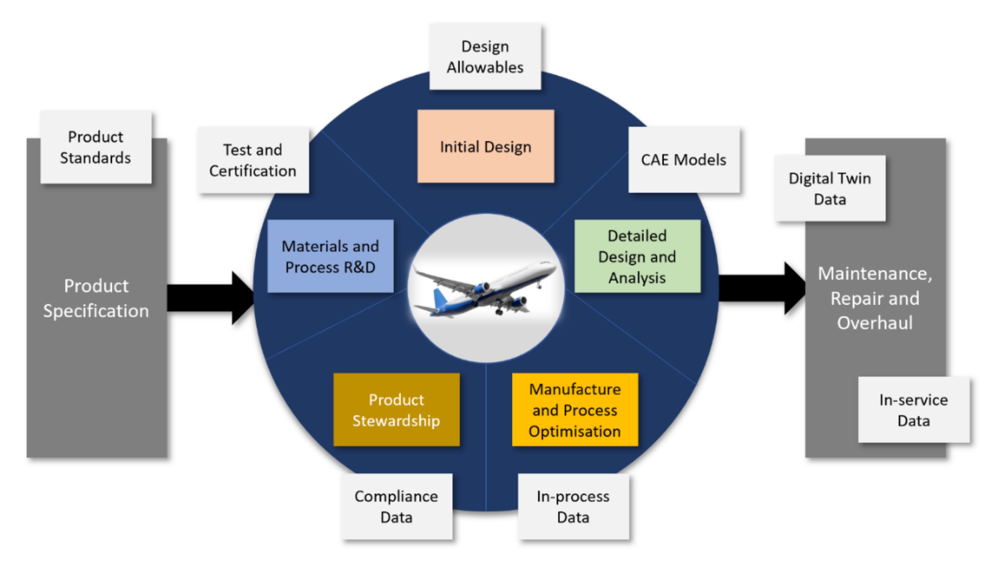
The choice of components, materials, design layout, housings, etc., and their interactions define the lifetime of a product. There is a massive amount of data involved in the development process and through-life maintenance of an aircraft vis-à-vis the various choices in terms of materials and components that need to made throughout the product design and development, as elaborated in
Figure 1. This implies that during the specification stage, it is essential to select requisite materials and components in a technically viable manner. Usually, this includes procuring components and materials that meet the standards of the specification. However, in innovating new technologies, this may rely on the development of new materials, processes, or components that will need to be certified to meet the standards by testing and certification routes.
This leads to a set of design “allowables”, that form statistically determined material property values derived from test data. These define the limits of stress, strain, or stiffness that are allowed for a specific material/component for given configuration, application, and environmental conditions.
Computer aided engineering (CAE) may then be employed to produce detailed design and analysis to show how the design allowables interact with one another. This may encompass simulation, validation, and optimization of the design using such tools as finite element analysis (FEA), computational fluid dynamics (CFD), multi-body dynamics (MBD), and durability, in addition to the optimization tools.
As the design evolves into the manufacturing stage, additional information becomes available to the design in terms of maintenance, repair, and overhaul in-service data which may be fed back into the design process, leading to changes and modifications to the design. This in-service data (ISD) is extremely useful in trend monitoring to track routine airplane performance using the parameters of flight hours and landings, component removals and failures, component no-faults-found (NFFs), airplane schedule reliability, and maintenance action rates. The processed data is also used to understand, in greater detail, what is driving the high-level trend data; for instance, if there is a change in the meantime between unscheduled removal for a particular component. In addition to trend analysis, the ISD may be used for new system development, including system improvements and requirement settings.
The huge variety of different materials and components used on an aircraft make product stewardship essential to managing the environmental impacts of different components and materials, and at different stages in their production, use, and disposal. Ensuring compliance is becoming increasingly important to modern designs. This design cycle highlights the need to explore innovative tools to improve the design process, in particular the initial and detailed design and analysis stages. Developing reliability into the design at this stage helps improve the overall availability and maintainability of aircraft systems.
Keeping the aforementioned in perspective, this paper presents how modern computer-aided engineering (CAE) tools can be used optimally to evaluate the overall reliability of an electronic system from an initial design, in this case an off-the-shelf power electronic evaluation module. We employ physics of failure (PoF), or reliability physics, which makes use of degradation algorithms that describe how physical, chemical, mechanical, thermal, or electrical mechanisms can decline over time and eventually induce failure. Utilizing PoF allows derivation of accurate predictions of the failure behavior of next-generation components, including silicon transistors, wire bonds, solder bumps, die attach, light-emitting diodes, electrolytic capacitors, plated through-holes, and solder joints.
Printed circuit board (PCB) modelling and simulation facilitates design failure mode and effects analysis (DFMEA) and thermal de-rating, for accurate selection of glass and fiber, and informing the overall material properties selection. In addition, identification of mesh copper features within PCB substrate materials helps identify potential risks. It also enables the simultaneous application of multiple environmental influences to test within specific parameters for materials, stack-ups, and lifecycle events (thermal, shock, and vibration) in finite element calculations and analysis for reliability predictions of all parts using validated models.
The remainder of the paper is organized into five sections.
Section 2 provides an overview of the related work.
Section 3 defines the physics of failure (PoF) in power electronics at the PCB level. The PoF-based lifetime prediction results are highlighted and analyzed in
Section 4 and
Section 5, respectively. The overall conclusion of this research work is presented in
Section 6.
2. Related Work
In engineering, the development of a model has been used traditionally to understand component failure mode progression. The development of PoF or physics-based models (PbMs), that incorporate the ability to assess damage to a component, taking into account operating conditions and giving a cumulative damage assessment, provides a basis to evaluate the distribution of the remaining useful life (RUL).
It is deduced from a literature review that the actual availability of physics of failure models is limited. This implies that, at present, few PoF models incorporate the ability to predict damage parameters with an acceptable confidence boundary over steady-state and transient loads, temperatures, and other variables. One such model that has found prevalence in prognostic literature is the Paris law for crack propagation [
1,
2]. Here, the crack growth process was simulated to yield normally distributed crack lengths, which were used within a Bayesian framework to update the parameters of the degradation model (e.g., Paris’ law). The degradation model was initially fed by the results of a stress analysis from a gear dynamic model or finite element model. The distributions of the uncertainty factors were updated via Bayesian inference using the condition monitoring data (simulated crack lengths), and an estimation of the RUL based on the degradation model was provided.
Kulkarni et al. [
3] proposed a physics-based (first principle) modelling and prognostics approach for electrolytic capacitors. Electrolytic capacitors and MOSFETs (Metal Oxide Semiconductor Field Effect Transistors) are the two major components that cause degradation and failure in DC–DC converters. The paper studies the effects of accelerated ageing due to thermal stress on sets of capacitors, with the focus on deriving first principle degradation models for thermal stress conditions. The degradation data forms the basis for developing the model-based remaining life prediction algorithm. Finally, the data is used to derive accurate models of capacitor degradation and use them to predict performance changes in DC–DC converters.
A PoF-based prognostic method for power electronic modules proposed by [
4] allows the reliability performance of power modules to be assessed in real time. A compact thermal model is initially constructed to investigate the relationship between the power dissipation and the temperature in the power module. This relationship can be used for fast calculation of junction temperature and the temperatures at each interface inside power modules. The predicted temperature profile is then analyzed using a rain-flow counting method so that the number of thermal cycles with different temperature ranges can be calculated. A reduced order thermo-mechanical model is also constructed to enable a fast calculation of the accumulated plastic strain in the solder material under different loading conditions. The information of plastic strains is then used in the lifetime prediction model to predict the reliability of the solder interconnect under each regular loading condition.
In [
5], the researchers suggested a lifetime prediction methodology for assembled PCBs using characteristic failure curves from a fracture mechanics-based model and the local loading simulations. They provided a viable replacement for the board level drop test (BLDT), however, they could not carry out the PCB lifetime prediction using accelerated testing methods and finite element analysis post simulations. Krueger et al. [
6] processed the solder fatigue coefficients and finite element analysis (FEA) using a MATLAB routine for the lifetime prediction of flip chip (fitted on a PCB) solder joints. They analyzed and compared the significant features of microstructural modification and crack paths under individual temperatures and vibration cycling, in addition to the combined loading experiments with the lifetime model built on the Coffin–Manson–Basquin relationship. Although the predicted lifetime of all the bump types was a good match with the experimental results, it did not involve investigation involving PCB stresses and associated coefficients and exponents, which could further improve the lifetime prediction.
In [
7], Shangguan et al. developed a board-level PoF model to estimate the RUL of a power board. They considered various failure modes of a high-speed railway transmission module comprising a power PCB and accordingly built a board-level PoF lifetime prediction model for single and multiple failure mechanisms. They determined the prediction accuracy of the proposed model was 85.48%, consequent upon validation with Simulink. More serious degradation is attributed to multiple failure mechanisms when compared to the single failure mechanism. The model, however, could be improved for more accurate and complete RUL predictions for a power PCB if environmental parameters such as temperature and humidity are also factored in.
3. Defining Physics of Failure for Power Electronics
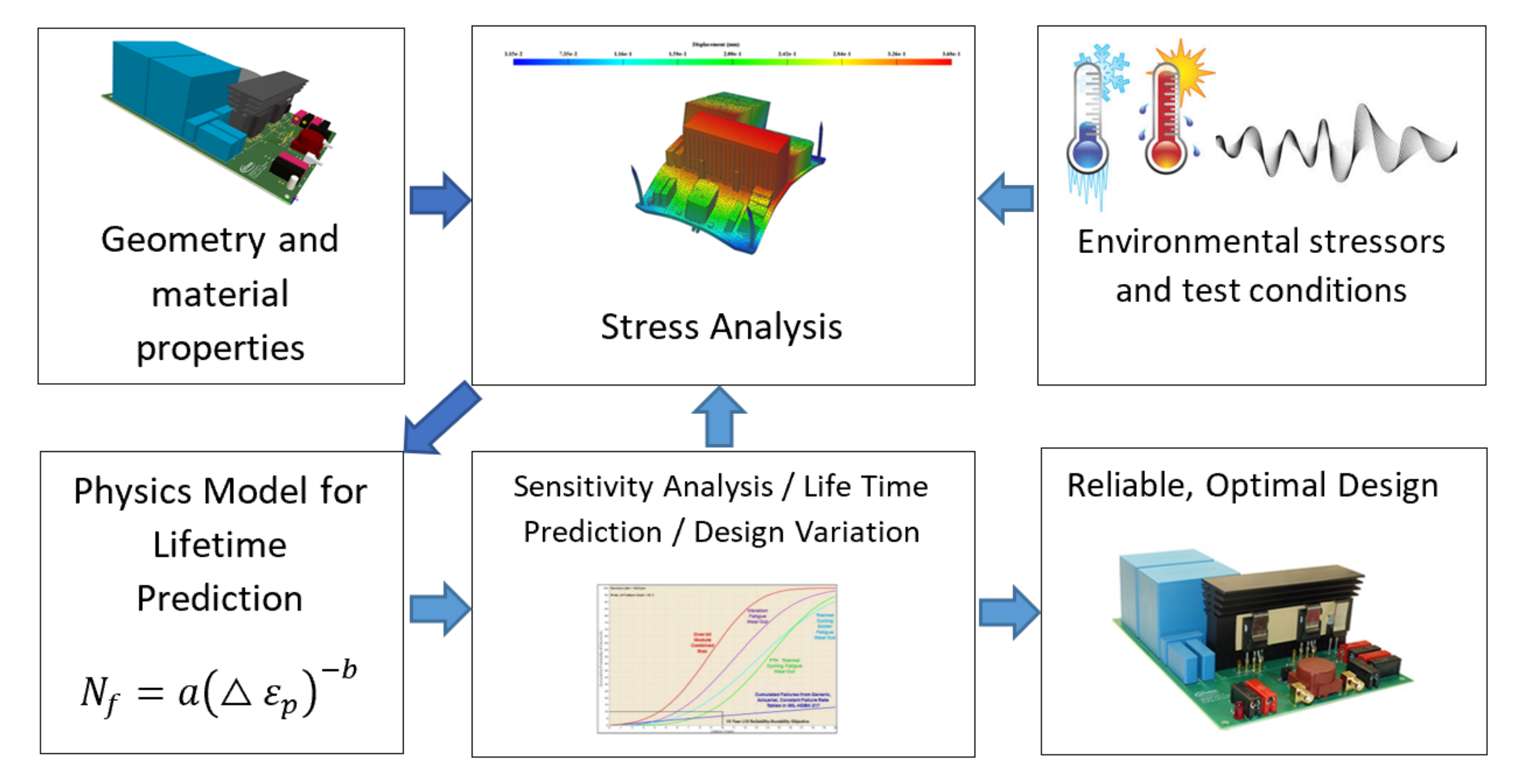
Figure 2 outlines the physics of failure methodology for assessing the reliability of power electronic components/systems. To begin with, the potential stressors are identified that lead to failure, such as thermal (events, cycling), mechanical (shock, vibration), chemical, electrical, physical, or structural stressors, which may lead to failure within the design. Secondly, the product is exposed to highly accelerated stresses, which may be in terms of a finite element analysis (FEA) for thermal and mechanical loads. Given an imported model of the design, the dominant cause(s) of failure is determined. Thirdly, by using models of the dominant failure mechanisms (of how and why the failure takes place), failure data is produced. Fourthly, data is gathered from acceleration tests according to statistical distributions, e.g., Weibull or log-normal distributions. Finally, mean time to failure (MTTF) and other lifetime predictions may be estimated and changes to the initial design may then be made if needed, with the processes being repeated until the reliability requirements for the design are met. Some of the PoF models and their description and applicability are given in
Table 1.
3.1. The Test Platform
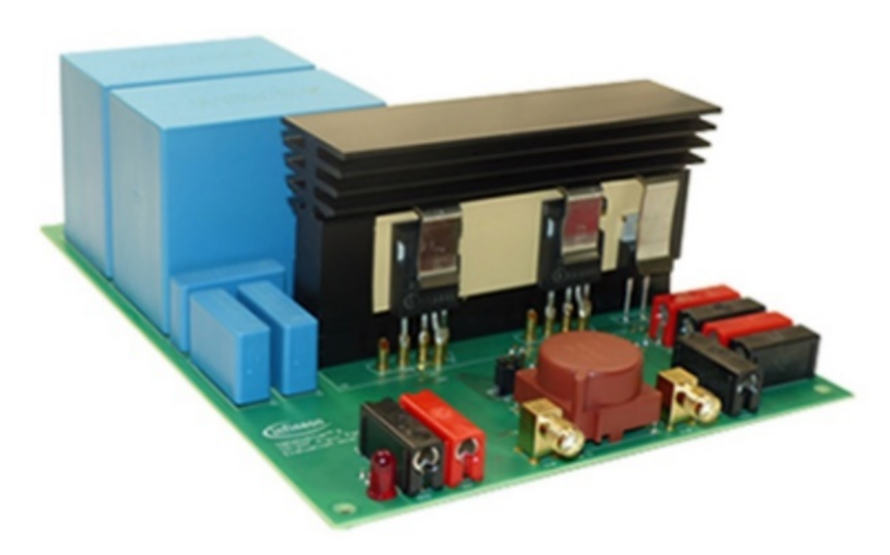
The test platform, shown in
Figure 3, is an evaluation board from Infineon [
8] and was developed to be a simple but accurate test bench for evaluating insulated gate bi-polar transistors (IGBTs) from the same manufacturer. The evaluation board makes it possible to measure the IGBT losses during switching events. It has an optimized layout, which features an overall commutation loop inductance below 35 nH, including packages and sockets. Different parameters can easily be set, such as load current, DC voltage, and turn-on and turn-off gate resistors. Case temperature can be adjusted through a power resistor implemented on the heat sink. The board can be used in continuous operation. From the basic phase-leg topology, it is possible to configure it as a step-down or step-up DC–DC converter [
9].
The multitude of different components, such as electrolytic capacitors, power devices, connectors, heatsinks, semiconductors, inductors, and transformers, make the platform an ideal test vehicle for evaluating CAE software. In addition, the board is also used in laboratory tests for thermal and vibration cycling within the department, making the eventual comparison of results possible.
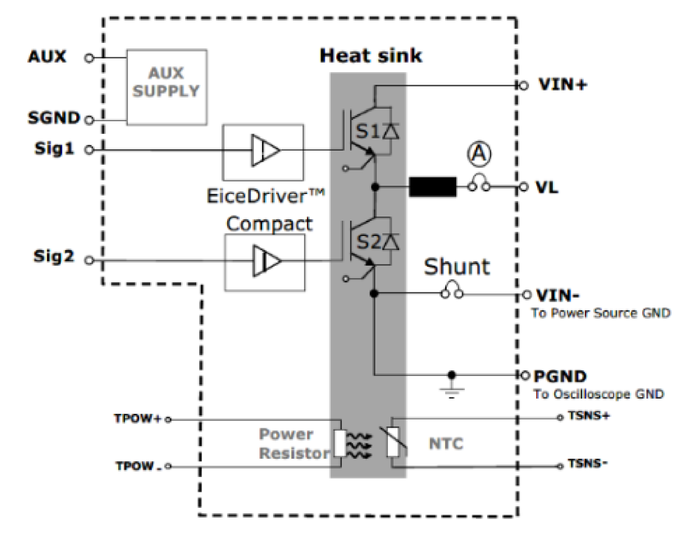
Figure 4 depicts the general block diagram of the evaluation board. It contains a phase-leg consisting of two IGBTs, S1 and S2, in either TO-247 or TO-247 4pin packages.
3.2. PCB Layout and Modeling
A 3D finite element analysis (FEA) model was created using the circuit card data extracted from 2D layer files, pick and place files, the parts list, and the PCB stack-up information. This was in the form of an ODB++ file generated by the PCB design software.
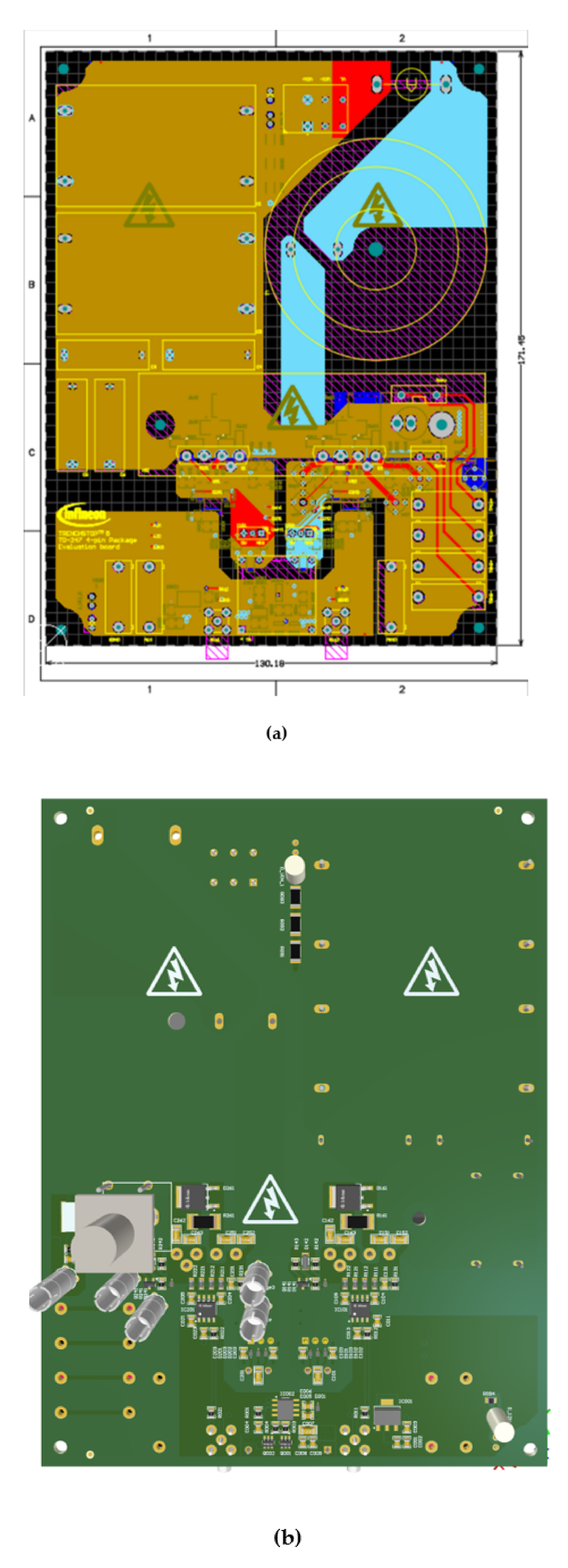
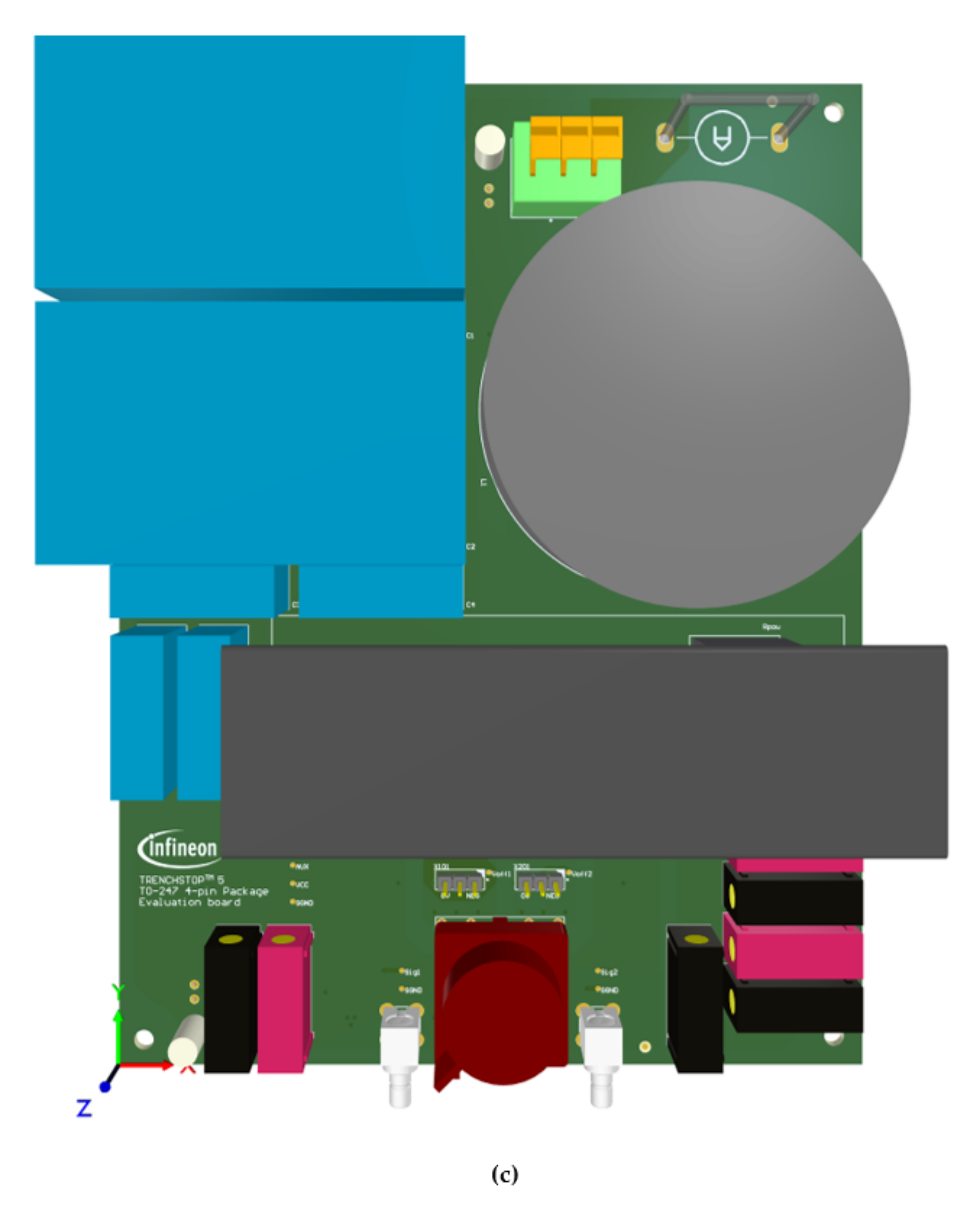
The PCB model was converted into an elemental model. The generated elemental model consists of a collection of 3D elements (either wedges or bricks) that fill the volume contained by the PCB outline, minus any holes or cut-outs. The shape of the elements is determined automatically using an internal meshing algorithm. Two types of elemental models can be generated, namely “Merged” or “Bonded”, to support a range of analysis approaches. In a Merged Mesh model, the PCB is meshed along with all the parts at the same time, thereby allowing PCB and part elements to share the same nodes. In a Bonded Mesh model, the PCB is meshed independently of the parts, allowing both the PCB and part elements to be more uniformly shaped. The original PCB design is shown in
Figure 5a and 3D visualizations of the board are shown in
Figure 5c.
Because the board is mounted on stand-offs, they are also incorporated in the final FEA model. The imported board, as shown in
Figure 5b, exhibits the position of components, holes, and mount points. The latter are important because they are required when the board undergoes harmonic, vibration, and shock analysis as a datum for determining the eigenvalues.
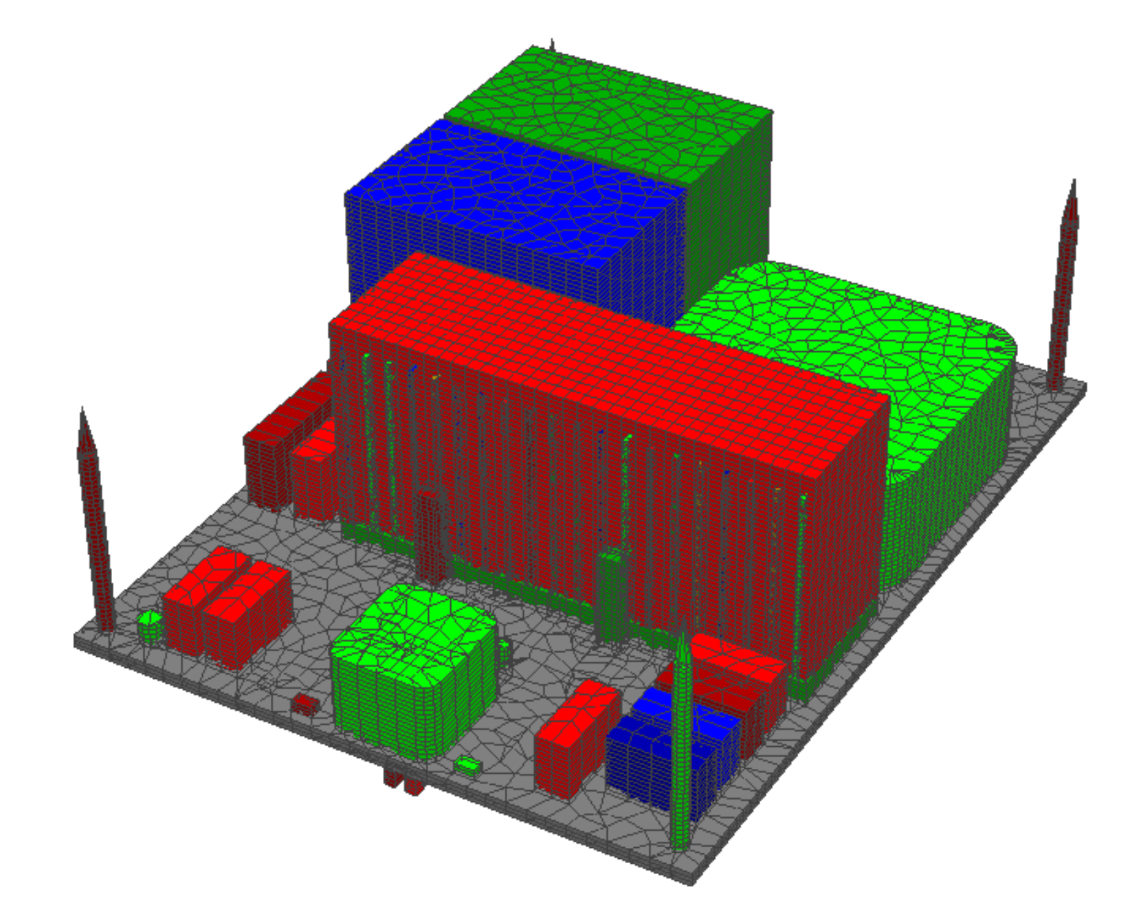
Finally, a generic FEA model, shown in
Figure 6, was created from the imported data and able to be used to analyze stress from heat, shock, vibration, and harmonics. This was then able to be fed into the appropriate physics models to allow a prognosis of RUL to be estimated.
3.3. The Test Plan
To provide a metric to evaluate the performance of the design, a suitable test plan needs to be devised. The following outcomes in the test plan should be addressed.
An overview of the PCB under test: This explains what the product does at a high level, how it is used in operation, and its key functions. The test equipment needs to be outlined, and usually a system diagram provides a basic block diagram overview of the main hardware components of the test equipment or automated test system. Because the tests are being carried out in a simulated environment, the equipment description becomes obsolete.
The test overview: This is a description of each test, including how the test is performed, the stimulus involved, how results are calculated, test limits, test time goals, the intent of the test, and the equipment involved.
The intent of the test: Why is the test being conducted? This should describe at a high level that aspects that will be tested. For a manufacturing test the testing of the unit should be scoped to ensure it is built correctly and adheres to critical design specifications. It should not be a design validation test.
The test limits: This defines a list of the limits for pass/fail. In reality, other parameters should be considered, such as test time, test equipment needs, test fixture needs, equipment lists, and capacity analysis.
3.3.1. Defining Test Standards
The test overview details for each test can usually be found in one of the many standards that exist for the testing of electronic equipment. Popular and trusted standards include: American Society for Testing and Materials - ASTM Testing Standards, Electronic Industries Alliance standard EIA-364 Electrical Connector Performance Test Standards, International Electrotechnical Commission standard IEC 60068-2 Electronic Equipment & Product Standards, International Safe Transit Association - ISTA Package Testing, Joint Electrostatic Discharge - JESD22 Solid State Device Packaging Standards, Military Standard MIL-STD-202 Electronic & Electrical Component Testing Standards, MIL-STD-331 Department of Defense Test Standards, MIL-STD-810 Environmental Engineering Considerations and Laboratory Tests, MIL-STD-883 Micro electric Device Testing Procedures, Radio Technical Commission for Aeronautics - RTCA/DO-160 Airborne Product & Equipment Standards, and Society of Automotive Engineers’ SAE J1455 Electronic Equipment Environmental Standards [
10,
11,
12,
13].
The outcome of the test may define the number of acceptable failures that can occur for a particular device/system; this is particularly the case for aerospace and automotive applications. For example, for an aviation system, depending on the criticality of the device on the operation of the aircraft, levels of acceptable failure are assigned:
Level A—Catastrophic: 109 failures/flight-hour
Level B—Hazardous: 107 failures/flight-hour
Level C—Major: 105 failures/flight-hour
Level D—Minor: 103 failures/flight-hour
Level E—No Effect: Not Applicable
It can be seen that level A corresponds to 1 in 1 billion failures per flight hour, which is an incredibly hard outcome to meet and may only be met in reality with a degree of redundancy in the system.
Hence, standards such as RTCA DO-160G
Section 5 [
14], for example, which deals with Temperature Variation Testing for Level A, are extremely stringent. This category is for equipment external to the aircraft or internal to the aircraft. The temperature variation testing is a minimum of 10 degrees Celsius per minute. Equipment meeting this description must undergo RTCA-DO-160 temperature testing from −55 to 125 °C in 15 min.
Table 2 outlines the hypothetical test plan for the PCB that was used as the test platform. For the majority of tests, MIL-STD 810 [
15] and IEC 60068 [
16] were used; these relate to equipment/components that are subject to day-to-day operational requirements. Other tests employed were based on Aerospace Recommended Practice standard SAE ARP 6338 [
17], EIA IS-749 [
18], SAE J3168 [
19], and Institute of Printed Circuits’ and Joint Electron Device Engineering Council’s Standard IPC-JEDEC J-STD-020D-01 [
20]. These standards are devised for semiconductor wear out, component failure, plated through hole and solder fatigue tests [
21].
3.3.2. Defining Performance Metrics
A product life-cycle defines the desired reliability goals and the various environmental stresses that the product (the PCB in this case) will see over its lifetime. These can range from simple to complex. These are then used by the analysis modules to predict PCB reliability and are set from the test plan or any specific mission profile.
For each set of results from the test plan above, a metric for pass/failure needs to be set for the board. Because the board is a commercial, off-the-shelf evaluation board for use in a laboratory environment, it cannot be expected to endure the stringent outcomes of aerospace and automotive applications. However, all of the components designated in the specification for the board are graded for −40 to +125 °C operation. The board also comes with stand-offs to support it during operation, which were incorporated into the models for completeness. To set pass/fail outcomes, it was assumed that the board has an expected operational life of 30 years with an assumed failure rate of 20%. This however, could be set in theory to be in terms of flight hours, cycles, mean time to failure (MTTF), mean time before failure (MTBF), etc.
4. Results and Analysis
The whole testing base is dependent on how well the PCB model is built and simulated under different stresses. The following stresses were, therefore, simulated on a well-developed PCB model to verify and characterize various impacts:
4.1. Thermal Mechanical Cycling Tests
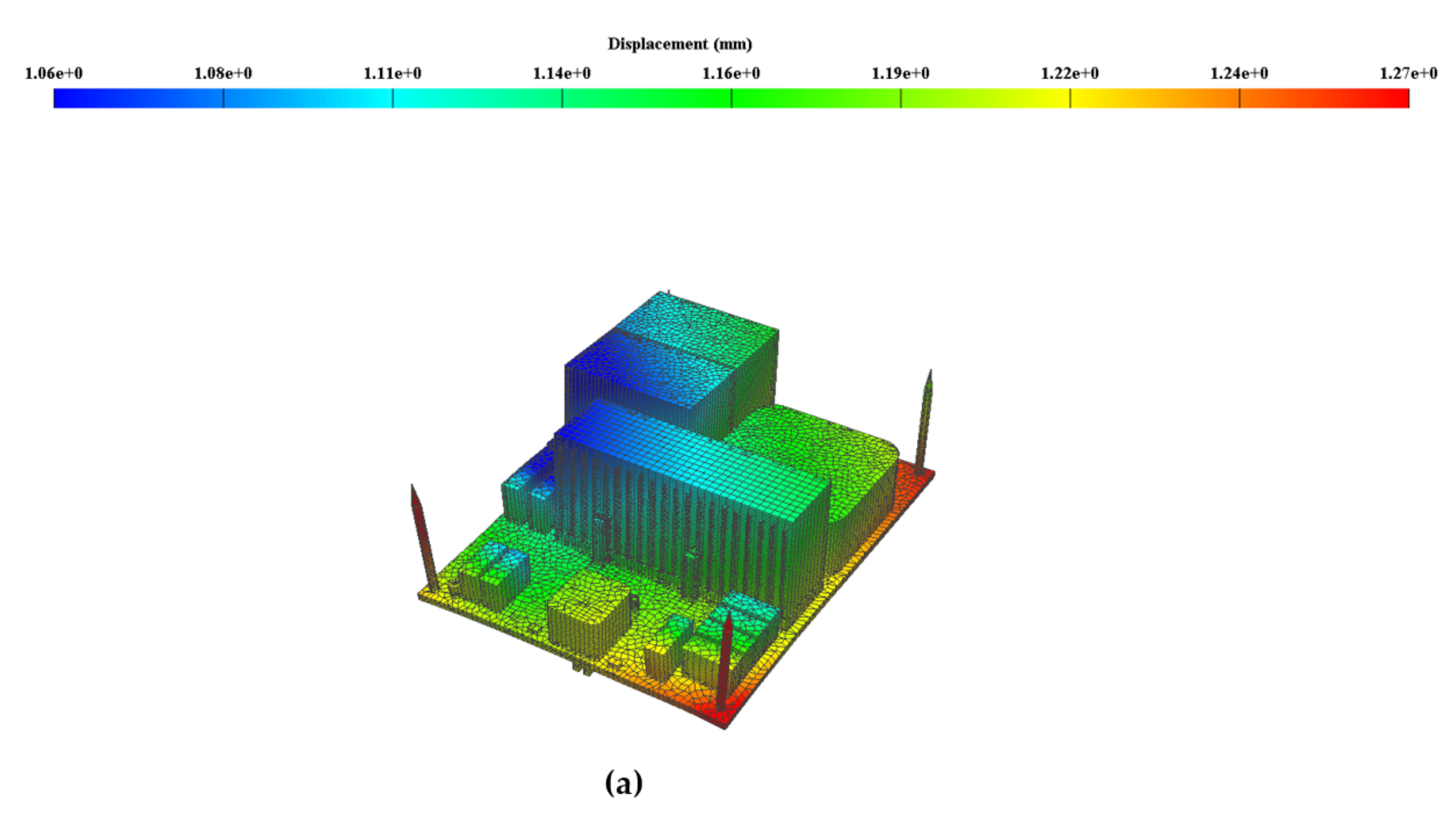
The initial testing involves one cycle from 30 min at the lowest temperature of −33 °C to 30 min at the highest temperature, 63 °C, with a maximum transfer rate of 1 min between the two extremes. The event component of this test involves three 24 h cycles, 30–43 °C while the circuit is operational, and three 4 h tests at −21 °C, again, while the board is operational. Finally, the test is repeated for three 24 h cycles, 30–63 °C, and three 4 h cycles, −33 °C, to replicate non-operational storage stresses. All tests were carried out under ambient air conditions.
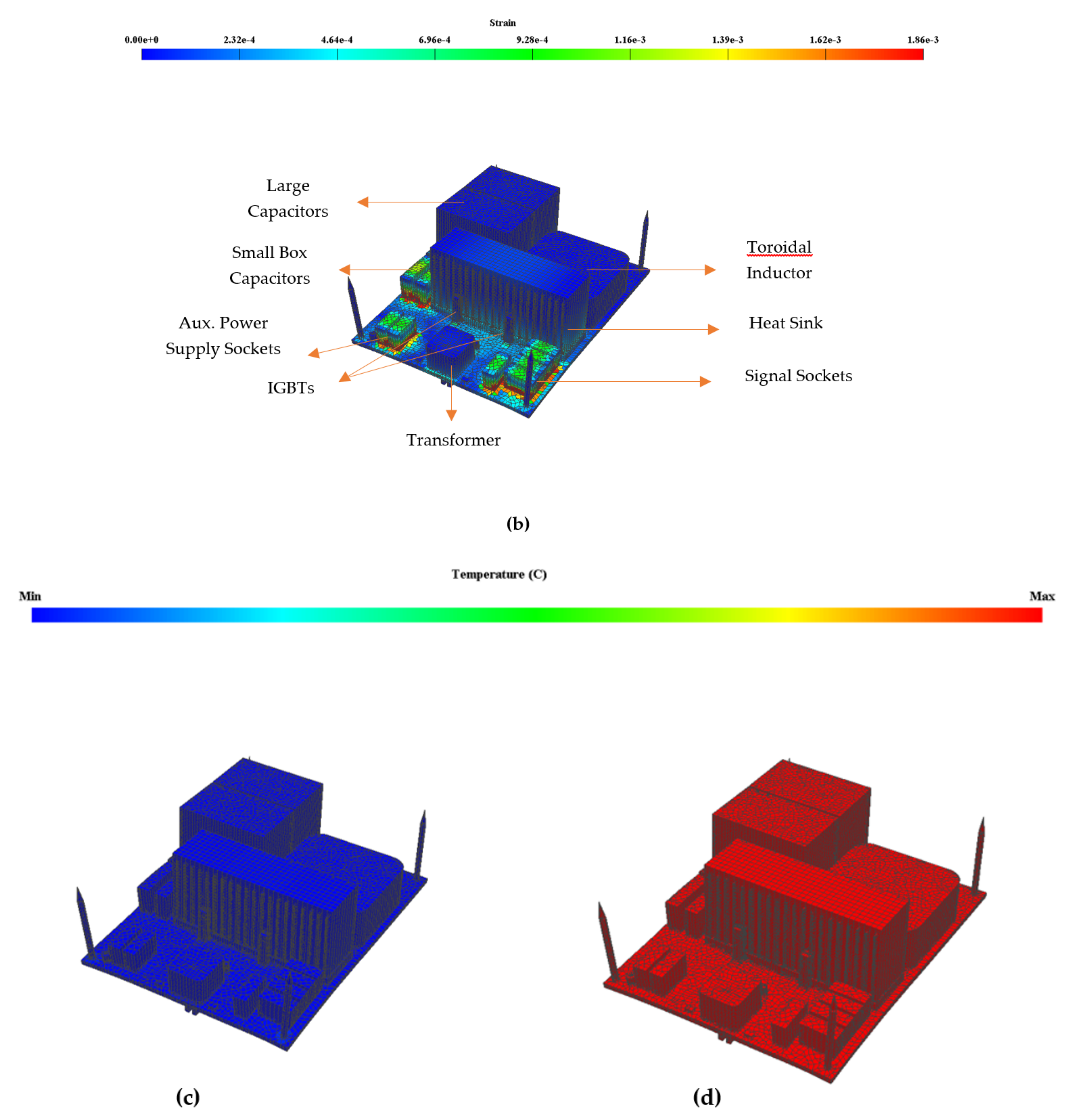
The results of the thermal mechanical cycling show that a number of components failed (indicated in red in
Table 3) or are at risk of failing (yellow). Examining the failures shows the large box capacitors, toroidal inductor, and connectors failed. More surprisingly, perhaps, transistors Q1, Q2, and Q001 also failed. Q1 and Q2 are supported against the heatsink and hence the failure may be due to the movement of the heatsink causing solder fatigue. By comparison, the box capacitors, toroidal inductor, and various test sockets/plugs are large objects made of plastic and metal having a high thermal expansion factor.
Figure 7a–d shows where the highest strain in the components was induced.
4.2. Thermal Mechanical Event Tests
Event tests are used to determine the effects of bias conditions and temperature on solid state devices over time. They simulate the devices’ operating condition in an accelerated manner, primarily for device qualification and reliability monitoring. The test consists of three 24 h cycles from 30–63 °C and three 4 h cycles of −33 °C to replicate conditions found in the storage of the device in ambient air conditions. This was repeated for three 24 h cycles of 30–43 °C and a further three cycles of 4 h at −21 °C, again carried out under ambient air conditions for an operational device. The results are shown in
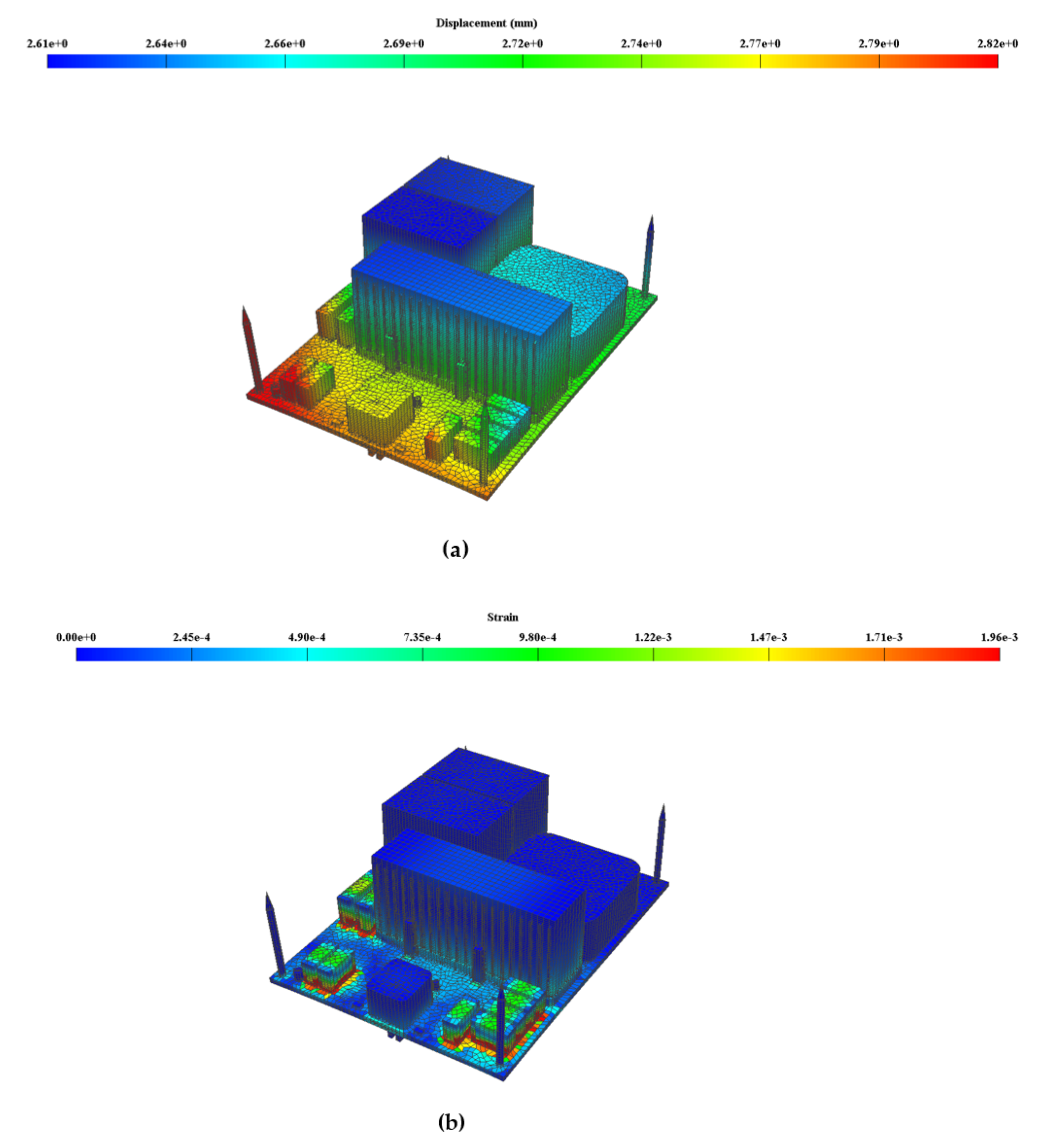
Figure 8a–c.
As can be seen from
Figure 8a that the thermal mechanical event stress at 63 °C is maximized with a displacement of 2.82 mm on the auxiliary power supply sockets. As a result, the auxiliary sockets may experience, during normal operation, some increase in the contact resistance, which in turn may cause voltage to drop, thereby impacting the boost function of the power board. Some high traces of stress are also observable on the edges of small smoothing connectors on the left side of the heatsink. In contrast, the remainder of the PCB (multi-layered board of FR4 laminate) and the components (heatsink, toroidal inductor, large smoothing capacitors, and surface mounted devices) remain within the safe regions of stress (<2.7 mm).
In
Figure 8b, the traces of thermal mechanical event strain at 63 °C are minimal around most parts of the PCB, except for the maximum displacement observable at the bases of the power supply and various signal sockets and the smoothing capacitors. However, no component failure was reported. It is, however, recommended to carry out condition monitoring tests after any such thermal mechanical event to determine any anomaly within the power switching function.
4.3. The Effect of Natural Frequency
The effects of resonance in numerous engineering problems are well documented and it is recognized that certain frequencies can cause catastrophic effects in structures such as bridges. This is also the case in electronics systems, and this test evaluates the circuit board and components against resonant effects. This was carried out by sweeping through a range of frequencies (10–2000 Hz) at an amplitude equivalent to a 10 G force. The test evaluates where the resonance was the greatest and displays the effects in terms of damage to the board at the frequencies of interest.
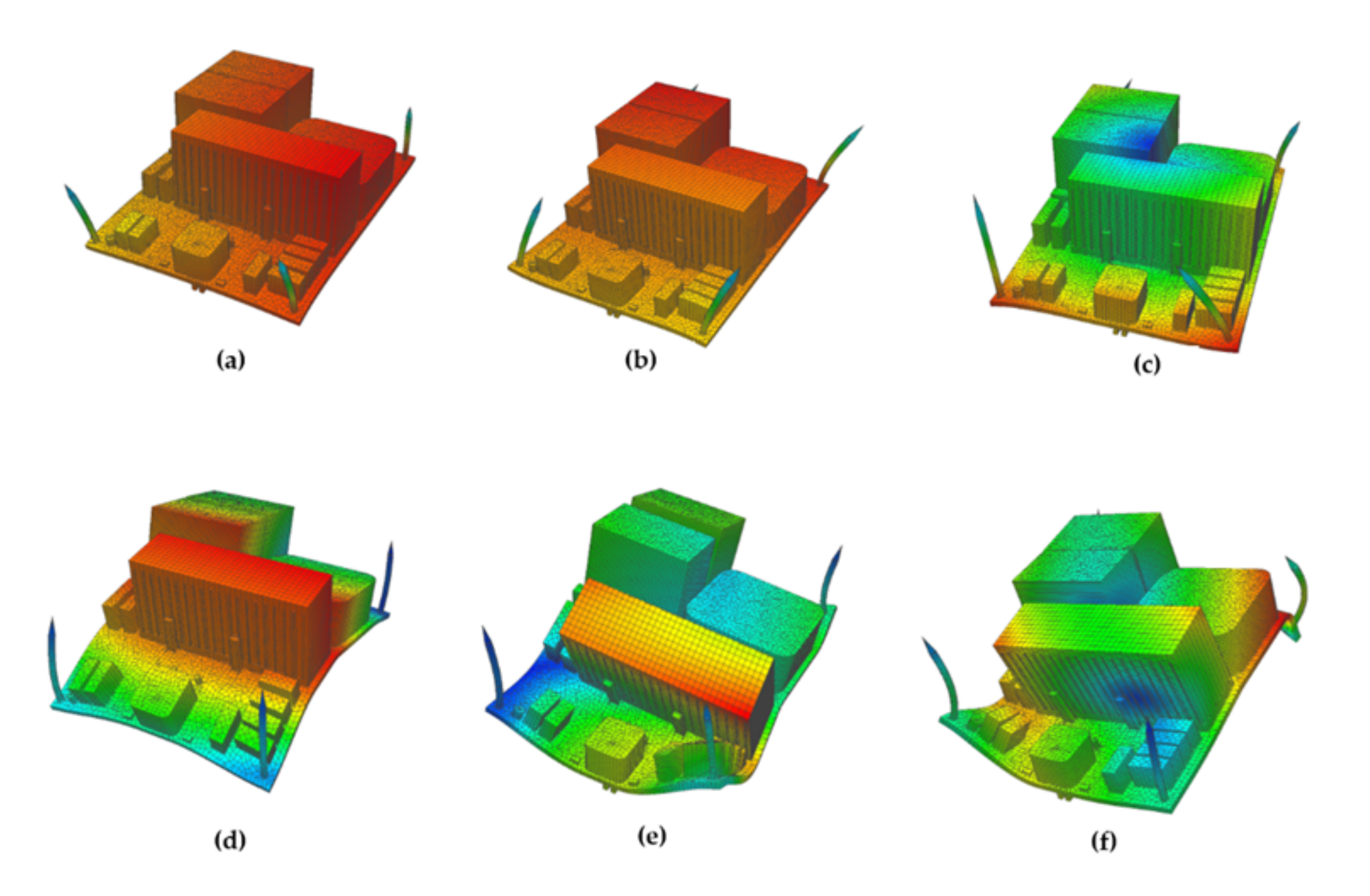
It can be seen from
Figure 9a–f that the resonant effects are small at the lower frequencies from 29.17 to 42.12 Hz. However, as the frequency increases, the damage incurred becomes much greater. At 212.75 and 222.69 Hz, the effects of resonance become especially pronounced in terms of stress/strain, and board/component failure would be eventually inevitable. Thus, mitigation would be needed, either in the form of avoidance of these frequencies (difficult in reality), or damping applied to the mounting of the board.
4.4. The Effect of Harmonics
Here, we want to show how the harmonics of natural frequencies mentioned in
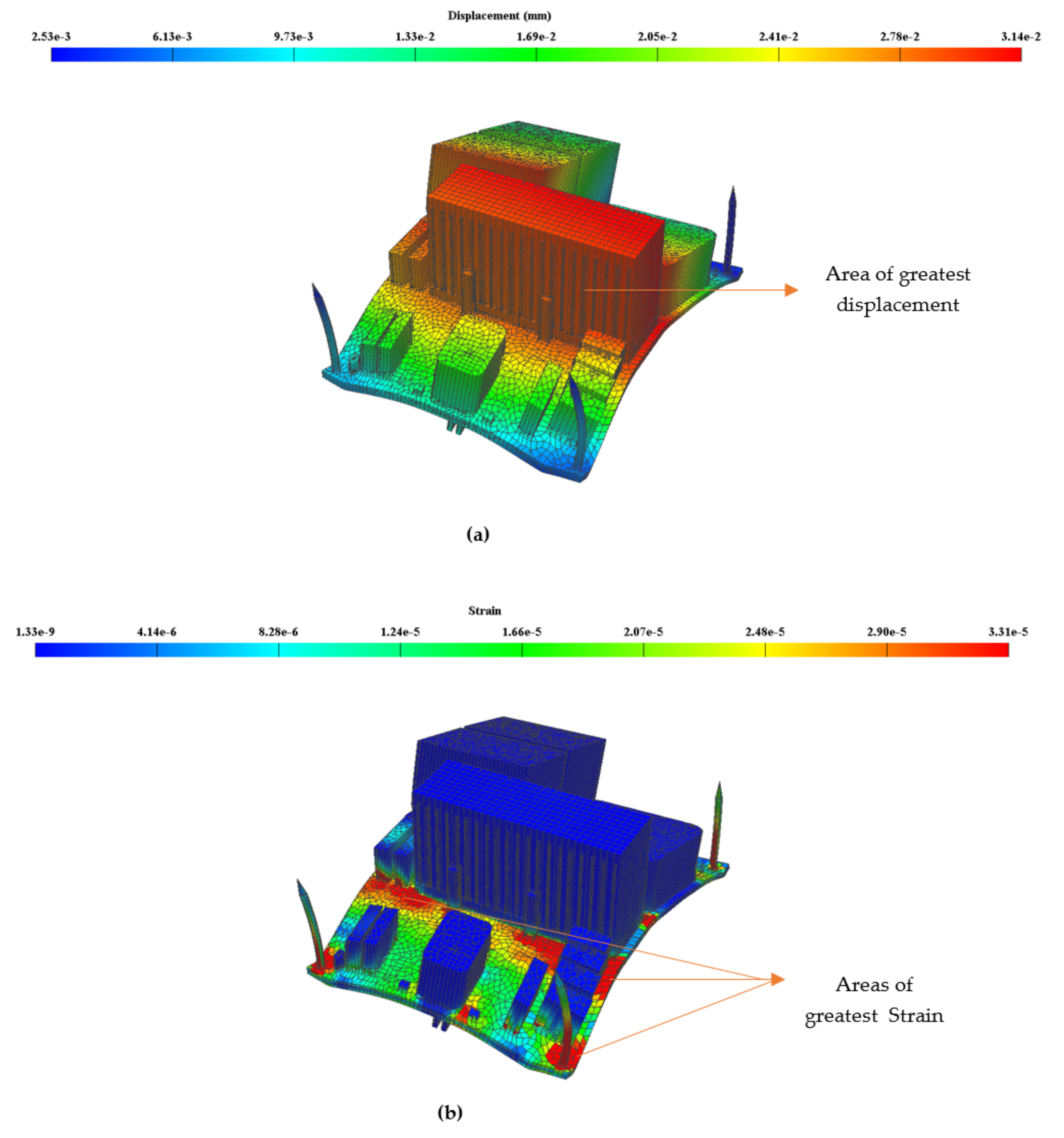
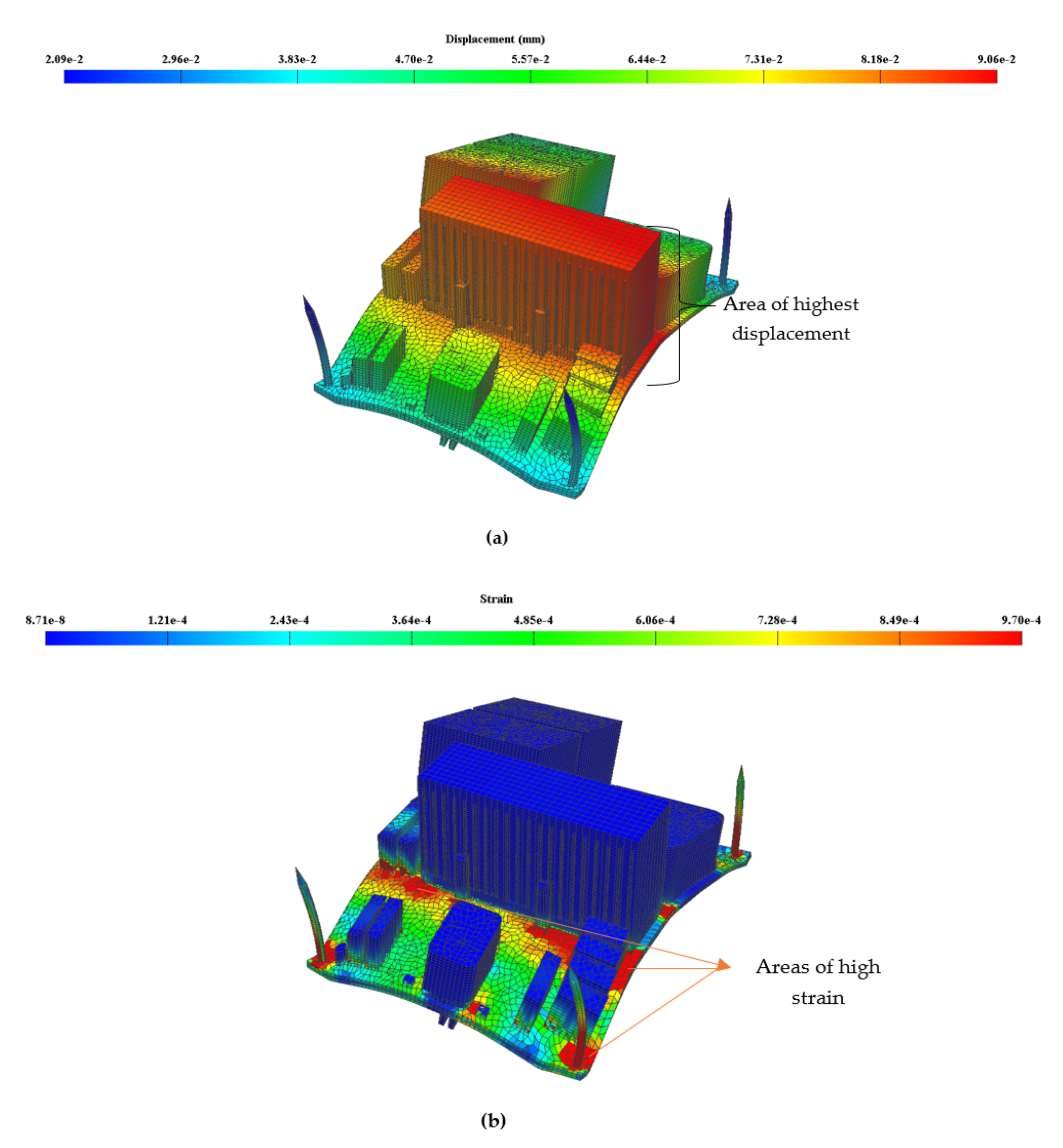
Section 4.3 impact the PCB in physical terms of displacement and corresponding strain. We primarily took 24.66 Hz as the fundamental natural frequency and observed the impact at its third-order harmonic of 73.98 Hz (which is the usual third harmonic observed within the aircraft system environment). Maximum displacement and strain occurred at 73.98 HZ and was used to calculate the lifetime of the device. From
Figure 10a,b, displacement and strain occur across the center of the board, either in the case of displacement where the heatsink is situated, or in the case of strain just in front of the heatsink. This transferred additional strain and stress into components situated in the vicinity of the heatsink, such as the capacitors, toroidal inductor, and transistors. However, from
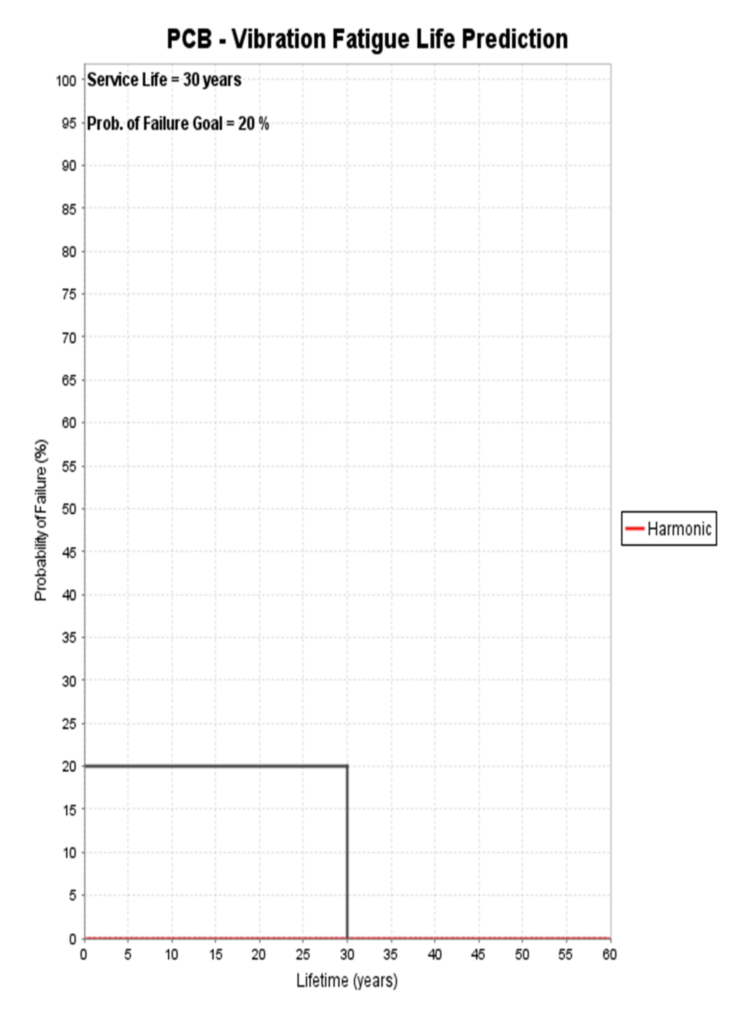
Figure 11, it can be seen that the impact of harmonics is not severe enough to cause a significant detrimental effect on the life of the board, with all components predicted to last well in excess of the 30-year lifetime with a probability of failure of 20% set during the analysis.
4.5. The Effect of Random Frequency
The random frequency analysis was subject to a triaxle agitation with a power spectrum of 0.04 G2/Hz from 20–1000 Hz and is subsequently increased by 6 dB for frequencies of 1000–2000 Hz to give an overall vibration of 7.7 G RMS (Root Mean Square). This was applied for a duration of 1 h while the unit was non-operational. This test is designed to emulate the broadband random vibration that equipment and products may undergo. Random vibrations can occur in operational environments, such as aircraft, space vehicles, and land vehicles, in addition to shipping transportation.
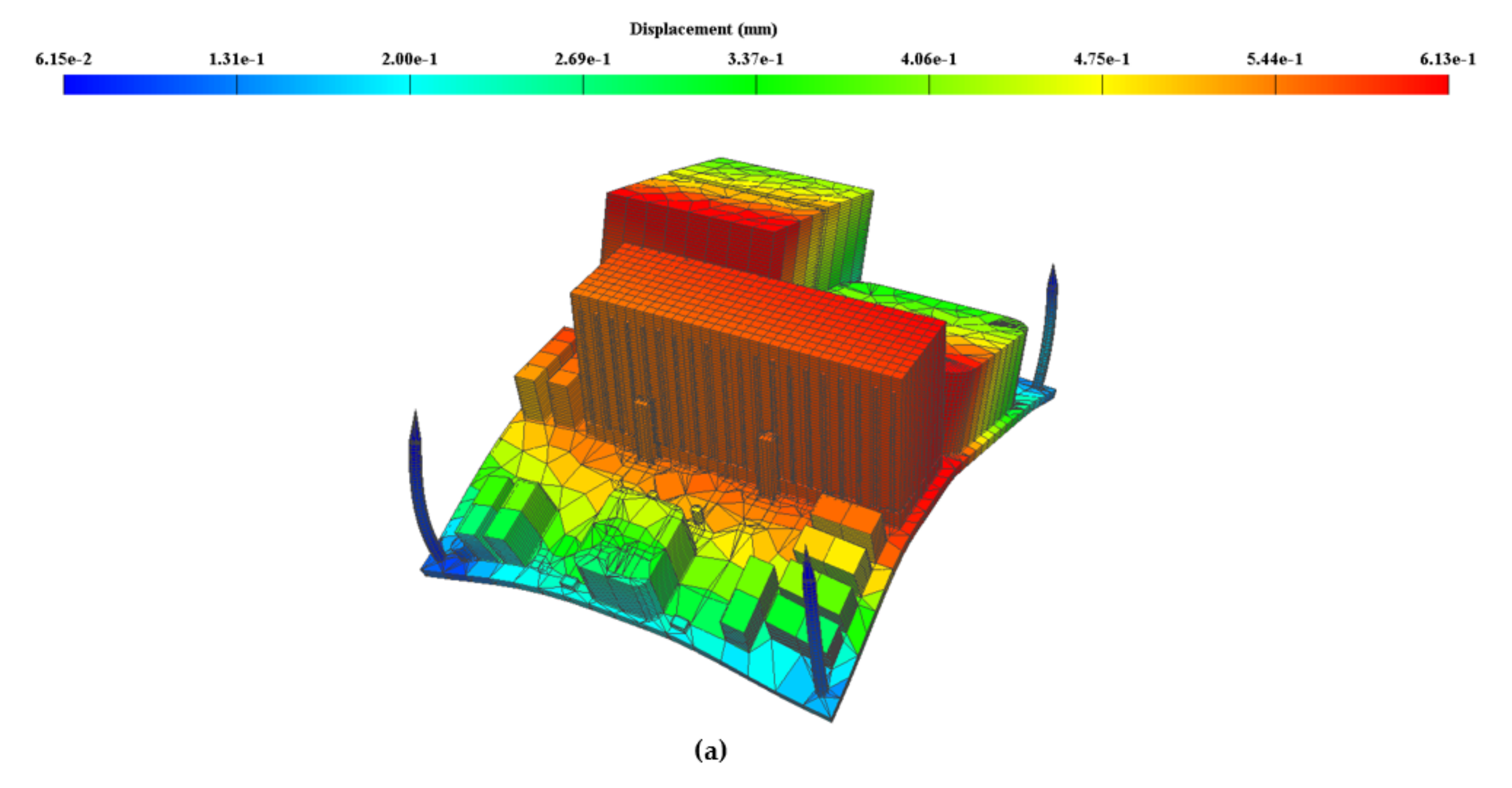
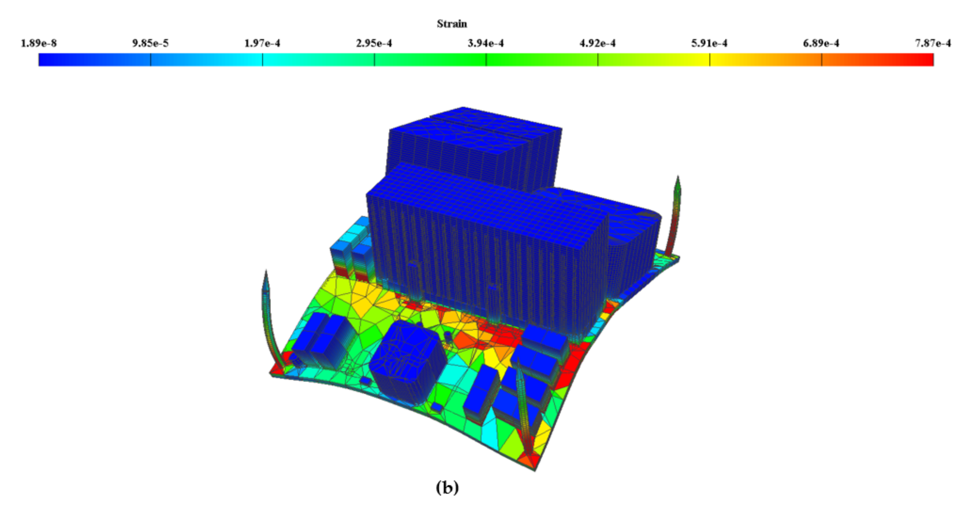
The results are again expressed as displacement and strain on the components and board due to the effects of the random vibration (see
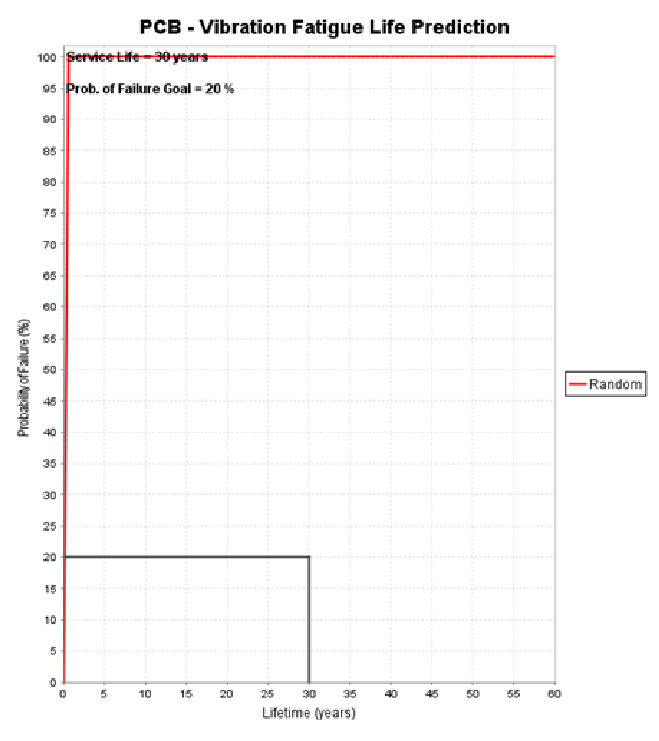
Figure 12a,b). The random vibration affected the board and components in terms of displacement and strain significantly more than harmonic vibration. This may due to the tri-axis nature of the agitation or magnitude of the stresses. Subsequently, this causes the failure of some of the components. Perhaps unsurprisingly, the components that failed were mostly the larger components situated at the top of the board, which, due to their size and mass, were subjected to more energy from the vibration. The PCB vibration fatigue life prediction is shown in
Figure 13.
4.6. The Impact of Mechanical Shock
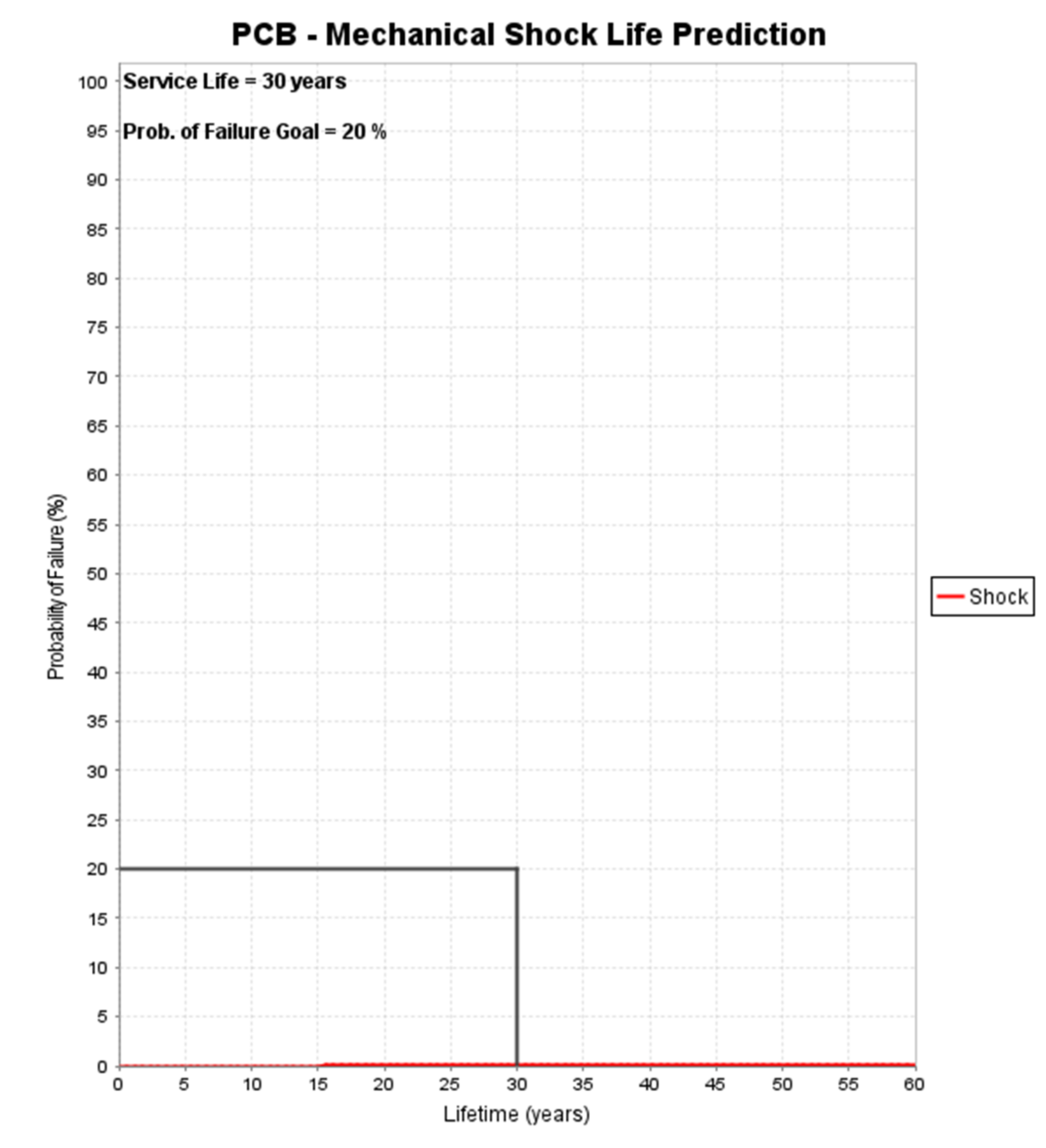
The mechanical shock test evaluates the structural integrity and the satisfactory performance of board and components that would experience steady or constant acceleration forces. The board and components were submitted to functional tri-axis shocks from a half sine wave for 6 ms at 10 G, for six shocks, and three pulses per direction. The results are shown in
Figure 14a,b. Again, maximum displacement and stress was exerted around the large central components in front of and around the heatsink, as one may expect. However, due to the short duration of the shock, all of the components survived the test and have a predicted life well in excess of the test pass/fail metric, as shown in
Figure 15.
4.7. Solder Fatigue
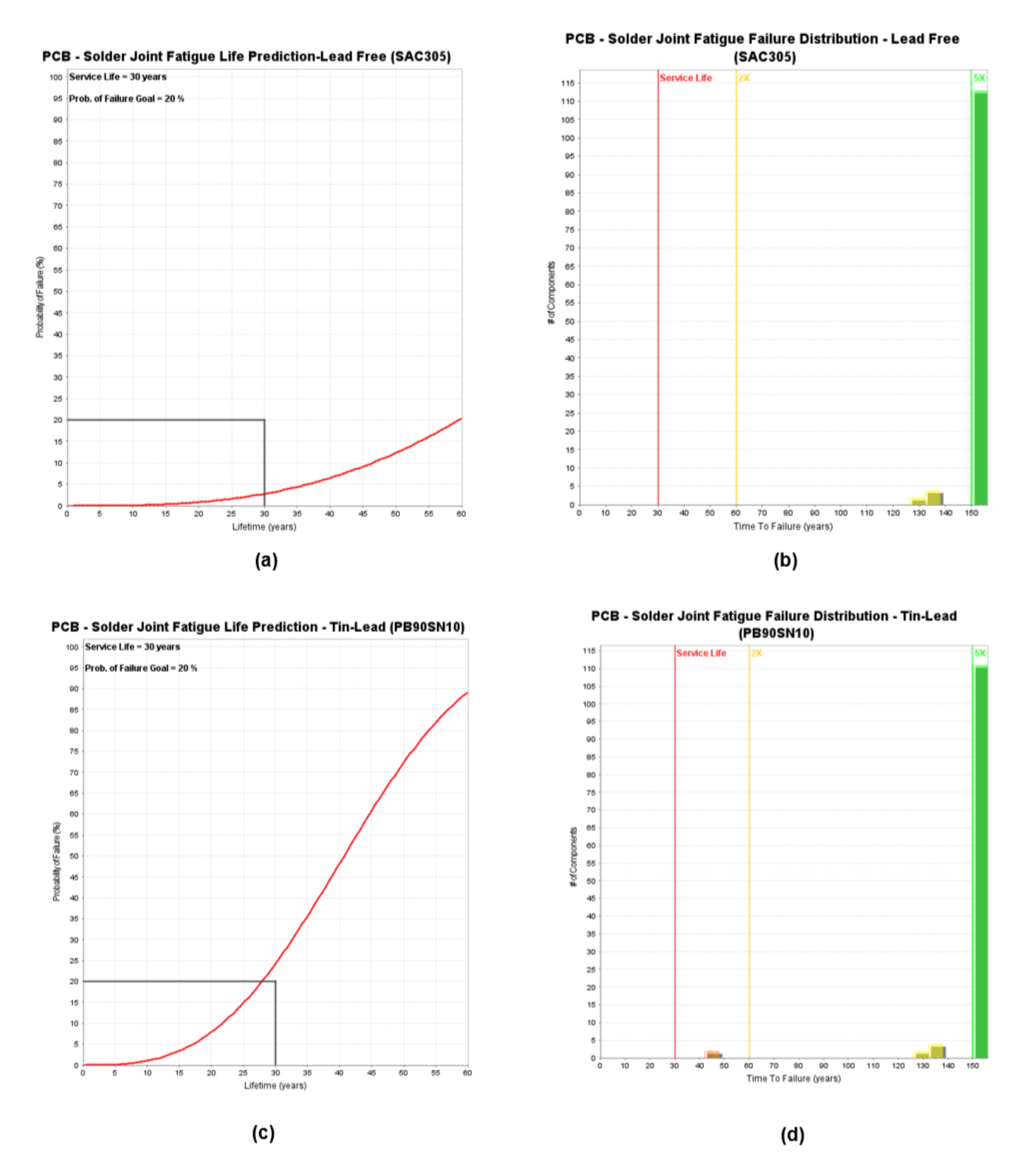
This test was based upon the IPC-JEDEC J-STD-020D-01 prediction equations for solder fatigue reliability under thermo-mechanical and mechanical environments for all electronic parts (die attach, BGA, QFN, TSOP, chip resistor, through-hole, etc.). It was carried out for two types of solders, SAC305, which is lead-free; and PB90SN10 which is lead-based. In each case, the tests were carried out for three reflow cycles, peak temperature = +260 °C.
From the results shown in
Figure 16a–d, all the of solders except PB90SN10 performed to the expected requirements for the board. The solder was deemed to fail on two components, namely Schottky D161 and D261 diode packages on the bottom of the board. This is due to the high degree of thermal mechanical strain experienced by the joint in this region. Interestingly, looking at the original board, both of these components are in the vicinity of the greatest strain and displacement, under the heatsink. Hence, to ensure that the design meets the design lifetime criteria, ideally the components should be moved, or at least a different solder than PB90SN10 should be used.
4.8. Semiconductor Wearout
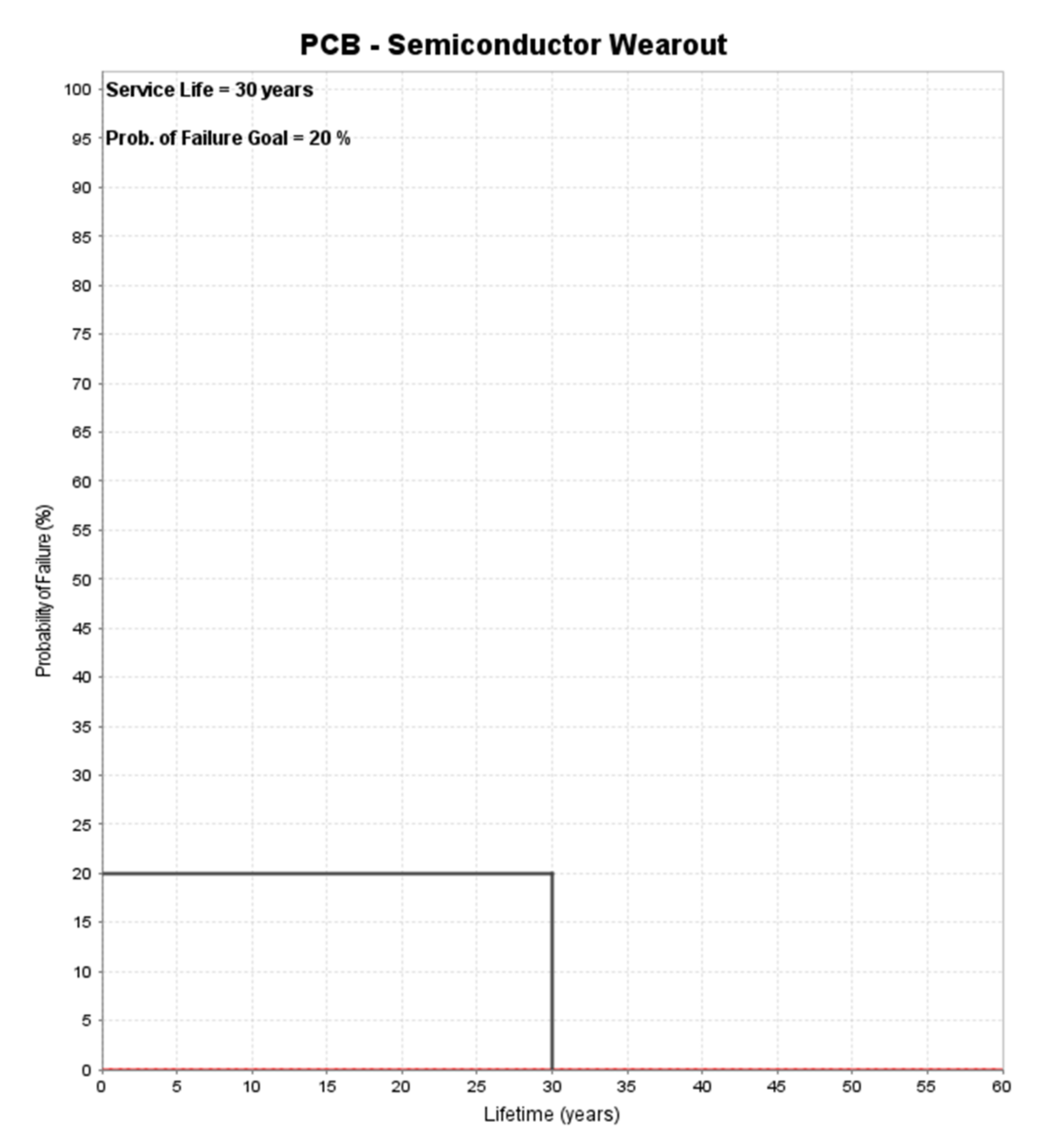
The semi-conductor wear tear is used to predict the failure rate and end of life of integrated circuits using degradation algorithms. Analysis includes electro-migration, time dependent dielectric breakdown, hot carrier injection, and negative bias temperature instability and is carried out in accordance to SAE ARP 6338. Four components on the board were subjected to this analysis, for both thermal cycle and events. In each case, the activation energy was defined as 0.9 and the appropriate operating voltage for each device was assumed. In each case, all of the semiconductors exceeded the life span of the board for the thermal cycle and event temperatures, as shown in
Figure 17.
5. PCB Life Prediction Analysis
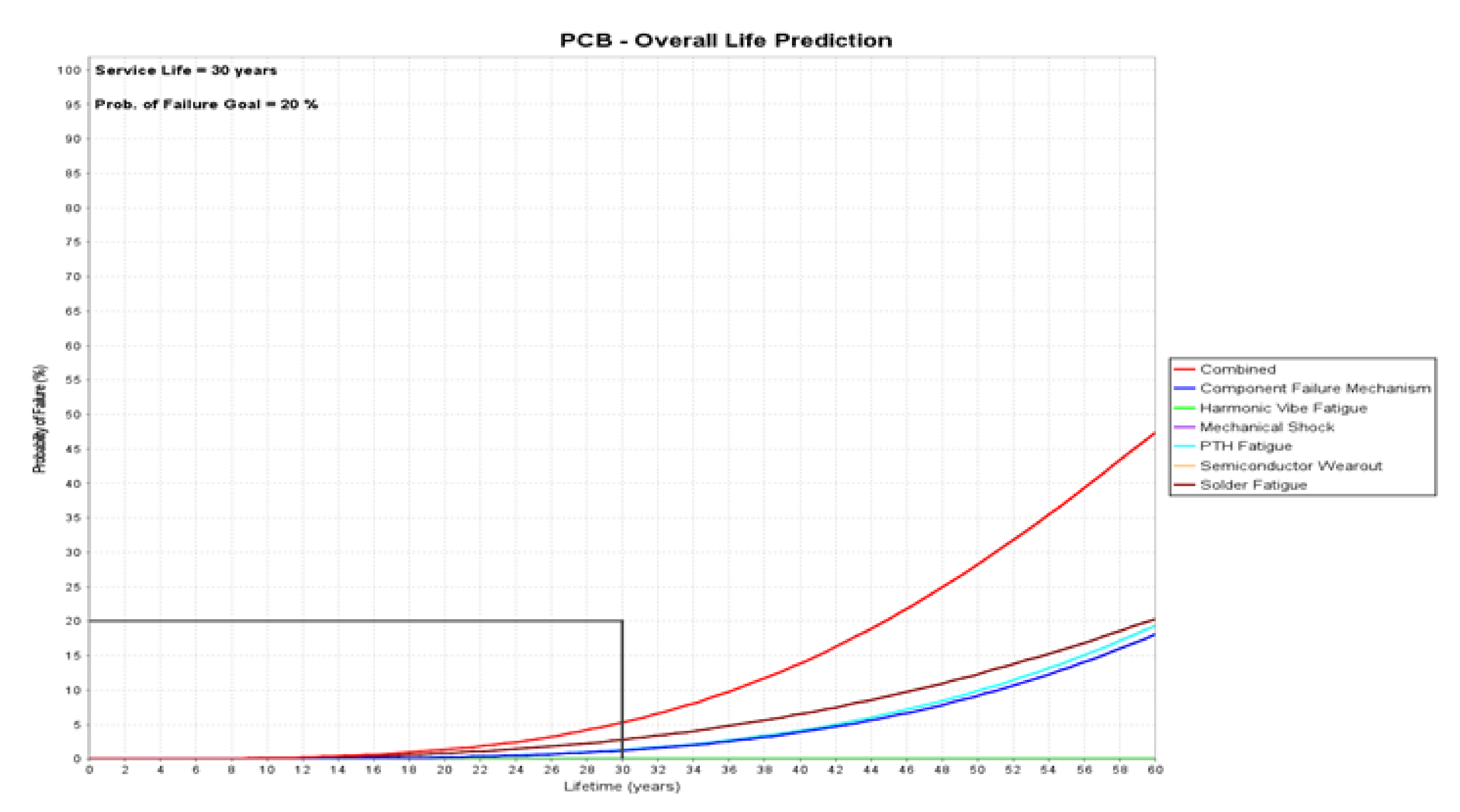
The overall life prediction for the board is shown in
Figure 18. Several concerns were highlighted that would need to be addressed from a design point of view. The first of these is the thermal mechanical strain, which caused a small number of the components to fail.
From the results, this occurred predominately for the larger components, particularly those in the vicinity of the heatsink and also manufactured from plastics that have a high expansion rate, e.g., test sockets and the large smoothing capacitors. The transformer and large inductive load also failed due to thermal expansion.
The actual board has some mitigation, such as the through-bolting of the inductor and retaining clips for the IGBTs mounted to the heatsink, which were not incorporated into the FEA model. The other test where failure was evident was due to random vibration. In this case the same larger components failed, because they were subject to more energy from movement. This would have been compounded by the fact the board was simulated using the lengthy stand-offs provided. Again, by providing mitigation for the vibration, in the form of damping and reduction in the stand-offs, this problem could be solved. The last point of interest in the results was from the solder fatigue analysis. All of the solders except PB90SN10 provided adequate resistance to fatigue for the given operational lifetime. This solder is a leaded solder that is still used in aerospace, military, and other safety-critical applications due to concerns over “tin whiskers”. The fact that some failure occurred highlights the importance of the careful choice of solder and that, despite having high confidence in the components, board, and design layout, the “glue” that holds the assembly is just as important.
The overall life assessment of the board yields a probability of failure rate of 5% in the 30-year life of the board. Addressing the concerns shown by the software and re-testing would see a further reduction in this failure rate, thus showing how design for reliability (DfR) can play a significant part in the design verification stage, thus saving time and money.
6. Conclusions
This study addressed the design for reliability (DfR) methodology by incorporating physics of failure (PoF) into the verification of the design of electronic circuit boards and troubleshooting of legacy boards. Numerous physics-based models and equations were explored, and how they may be used with simulated FEA stresses to produce a life assessment of the system for given testing standards or operational parameters. It was also shown how an existing PCB design may be used as the basis for the FEA model, by importing an ODB++ manufacturing model from the PCB layout.
The results from a test subject in the form of a power electronics evaluation board were used to demonstrate the process, and the board’s design was imported from the PCB layout and subjected to numerous tests. The results of these tests were then discussed and various conclusions around the design were drawn, illustrating the DfR process.
In summary, this physics of failure approach is part of a design for manufacturability (DfM) and design for reliability (DfR) methodology. By understanding the manufacturing risks, such as solder reliability, strain measurement, suppliers, material selection, and post-assembly operations, in addition to understanding the processes and mechanisms that induce failure, product performance can be improved. An early insight into the various reliability problems translates into almost immediate identification of areas of concern at the design stage, thus allowing issues to be rectified and designs to be retested before certification. This results in improvements in metrics such as safety, flight hours and landings, component removals and failures, component no fault founds (NFFs), airplane schedule reliability, and maintenance action rates.
