1. Introduction
5G and its evolutions enable new use cases such as industrial automation, mission critical Internet of Things (IoT), and advanced consumer services like virtual reality, augmented reality, and gaming with outstanding user experience. These new use cases will create additional revenue streams for Communication Service Providers. However, these new services require an adaptation of the network and its operations. In order to provide a good level of connectivity everywhere and among every point, the traditional network segments are evolving towards “one network” where the mobile infrastructure will be able to support any service, including enterprises, and the fixed infrastructure will evolve to also support mobile traffic. Such a new network segment where 5G mobile transport, fixed access, and vertical services converge is often referred to as Xhaul [
1,
2].
To comply with low latency use cases, some mobile core network functions need to move to the access. Traditional big data centers, in regional network segments, will be replaced by smaller ones, located closer to the antenna sites. Moreover, the transport network is evolving, replacing point to point physical connections, common in the access area, with rings, tree o simple mesh transport networks.
The mobile core network is evolving as well, becoming cloud native to allow new services to be created faster and in a more agile way. However, while some network functions will run on generic processors, other functions will remain implemented on dedicated hardware and managed as regular physical network functions (PNF).
In addition to 5G and IoT, other technologies, such as the Software Defined Networking (SDN) and Network Function Virtualization (NFV), will contribute to deeply transform the business of new digitalized industries. SDN facilitates the management and configuration by applying the software approach in all network operations. NFV allows to decouple the network functions from the proprietary hardware appliance, by using functions as Virtual Machines (VMs). Moreover, NFV uses Information Technology (IT) to partition the networks into virtualized building blocks that link up to produce communication services. As soon as industries introduce virtualized and software-defined infrastructure to expand their business in the digital economy, network automation will become essential to re-scale and re-purpose their operations.
The concept of “one network” targets End-to-End (E2E) network management, encompassing the entire network: radio, transport, and cloud resources. The access network segment will require not only higher bandwidth and lower latency than today, but also a higher level of automation, comparable with that of the other segments. Today optical communication technology can meet in principle high bandwidth and low latency requirements, however an enhanced level of automation is needed to enable the realization of networks that are managed E2E automatically as “one network”. Moreover, just scaling down in performance and cost the optical technology used in today metro and aggregation networks could be insufficient, since the capillary distributed terminations of the new access network will demand much smaller equipment size, energy consumption, and cost.
Silicon photonics are promising for this purpose, but they have been utilized, so far, mainly for datacom applications, e.g., to provide internal high bandwidth connectivity in data centers, that present different requirements with respect to telecom applications. Achieving a high level of automation at a suitable cost and size is one of these requirements. There are promising research results addressing this aspect [
1] but not yet large-scale industrial investments.
In this paper, we will discuss the new transport requirements in the access network, focusing on an implementation based on integrated silicon photonics. In
Section 2 the reference network scenario and the main requirements are reported; in
Section 3 a survey of silicon photonics technology is presented with the main challenges and potentialities;
Section 4 and
Section 5 provide two examples of novel enabling silicon photonics components and their design issues: tunable optical filters and Reconfigurable Optical Add Drop Multiplexers (ROADM), respectively. Conclusions are in
Section 6.
2. Reference Network Scenario and Main Requirements
The transport network requirements depend on both the E2E services to support, such as IoT, and the type of radio architecture. In a radio split architecture, the different layers of the protocols stack are allocated in different nodes, instead of being all in the same base station.
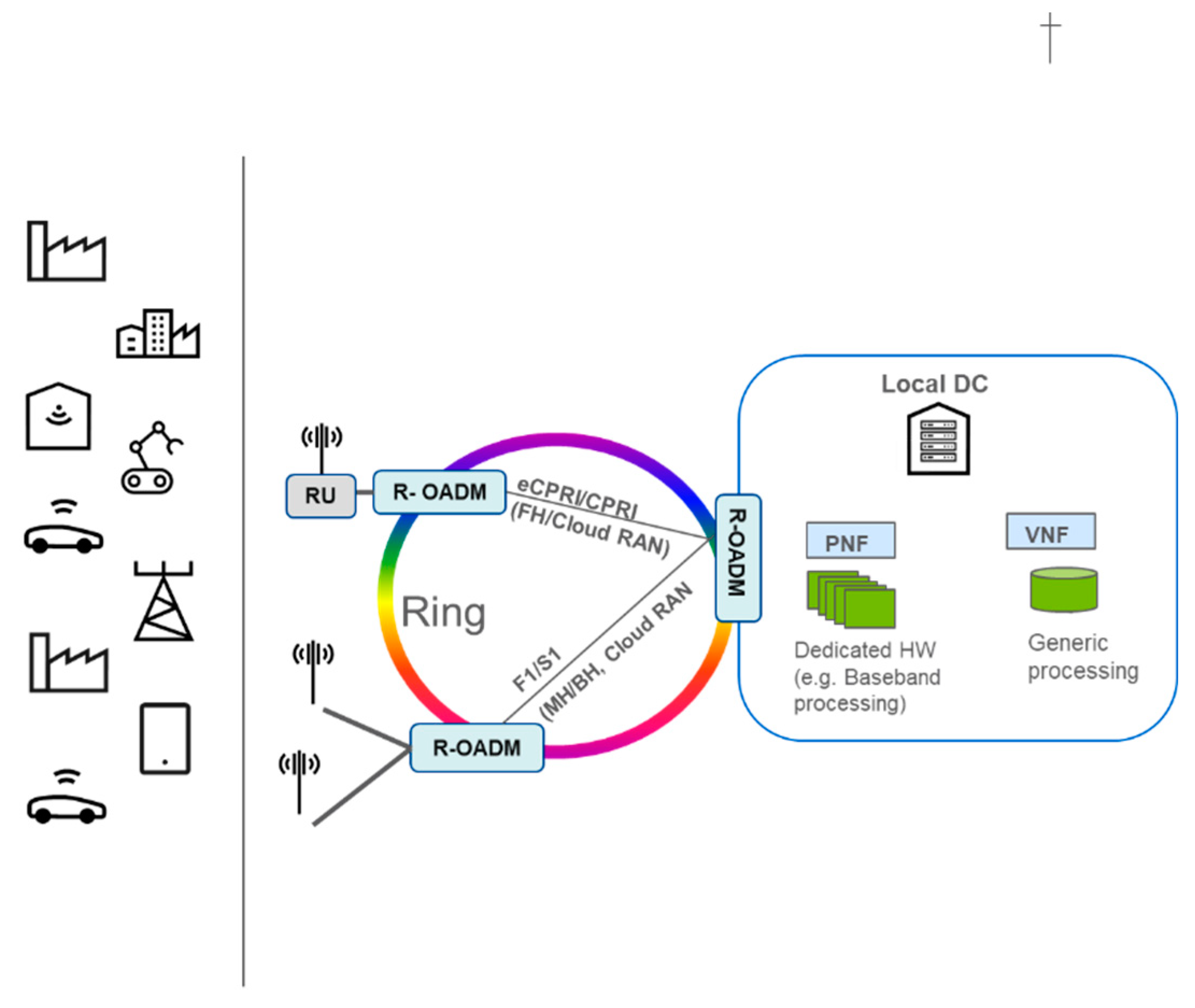
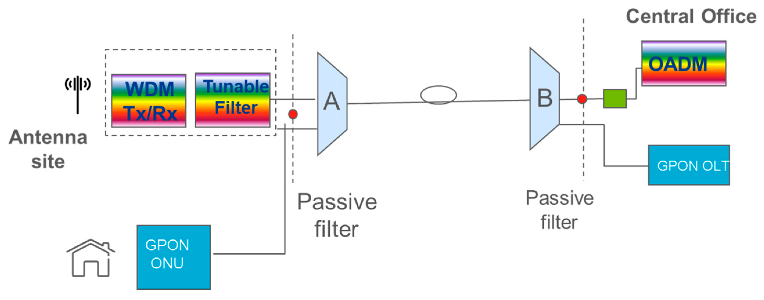
Figure 1 reports a reference scenario for an access network able to support mobile transport features with alternative radio splits, concurrently supported. As shown in
Figure 1, common topologies in this access area are Passive Optical Networks (PON) and ring optical networks.
In this scenario, the antenna sites are connected to the Central Office (CO) using different radio interfaces, each one corresponding to a different protocol split: CPRI [
3], which is the most critical in terms bandwidth and latency requirements; eCPRI [
4], which requires less bandwidth but has similar latency requirements of CPRI; and S1 [
5] and F1 [
6] that have less demanding bandwidth and latency specifications. The CO hosts both VNFs and PNFs (Physical Network Functions). For the sake of simplicity, in
Figure 1, the radio interfaces are shown in the ring topology case, but the same traffic applies to the PON.
An efficient transport infrastructure should be able to accommodate different services, as well as different radio split options. This concept is usually referred as Xhaul [
7]. In [
7], alternative Xhaul implementations are reported, including a case where PON physical infrastructure is used, but not its Time Division Multiplexing Access (TDMA) protocol. Wavelength Division Multiplexing (WDM) has several advantages for the implementation of an Xhaul infrastructure: it is transparent to the different radio interfaces, it maximizes the transported capacity over optical fiber and has low latency [
7]. However, a key aspect for enabling the path towards NFV is to provide a suitable level of automation. Automation in PON and rings presents peculiar requirements that will be better detailed in the next sections.
2.1. WDM Overlay in PON
In most cases, network operators would like to reuse installed PON infrastructure to carry mobile traffic. This allows to exploit the existing infrastructure, saving the high cost of new installations. The topology of a PON is point-to-multipoint, i.e., a “tree” that connects the CO with end user sites through a power splitter. A WDM overlay on a PON [
8] is a good solution to support several radio splits, especially in the case of low latency requirements and high bandwidth traffic, such as CPRI and eCPRI [
9]. With the WDM overlay, the same fiber transmits the PON upstream and downstream channels and the WDM channels over a separate spectrum [
8].
Figure 2 shows a PON with WDM overlay. The distance between CO and antenna site depends on the operator infrastructure: it is typically 5–10 km in densely populated areas.
Bidirectional operation (i.e., using a single fiber for both propagation directions) is another important feature of the network scenario in
Figure 2. It simplifies the network installation and configuration, that can be done “plug and play”, without taking care of the different fibers used in uplink and downlink.
The key device to provide a first level of automation in such a network is a full tunable Transceiver (TRX), at least at the PON termination site. As shown in
Figure 2, the WDM comb is transmitted from the CO to the antenna site, where a tunable optical filter at the receiver selects the right wavelength. Today, most WDM networks make use of fixed optical filters, which impacts inventory and network configuration complexity. To reduce the TRX cost, direct detection is preferable to coherent transmission [
10]. The bit rate of interest in an Xhaul network to carry CPRI and eCPRI channels is 25 Gb/s [
11]. Tunable direct detection TRX at 25 Gb/s are commercially available but they support tunability only in the transmission function, by means of tunable lasers. All current technologies to realize tunable filters at the receiver, such as Micro Electro-Mechanical Systems (MEMS) [
12] or liquid crystals [
13], are not complaint with the TRX requirements in terms of size and cost. Tunable TRXs developed for the New Second Generation PON (NG-PON2) only support 4–8 WDM channels [
14,
15] while the number of channels should be much higher in a fully automated Xhaul network, for example 20 WDM channels with 100 GHz frequency spacing, according to the ITU-T standard frequency grid. As shown in
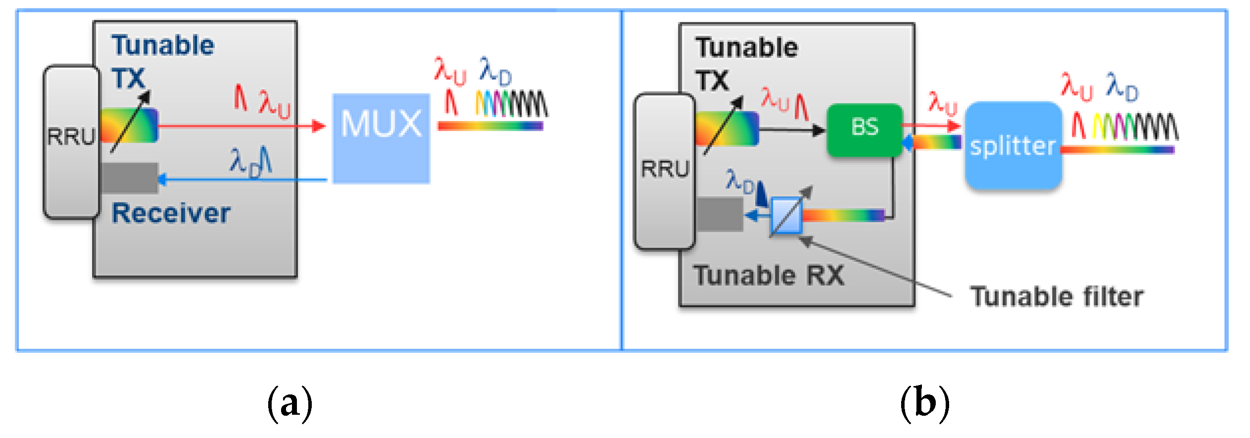
Figure 3a, a conventional TRX, where only the transmitter is tunable, works only if it receives one wavelength that has been previously selected (e.g., from a MUX in the
Figure 3a). This is due to the fact that it cannot select the wavelength from an ingress WDM channel comb. Hence a conventional TRX does not work in a PON infrastructure based on power splitters, where no wavelength selective optical devices are present (
Figure 2).
Figure 3 shows the compatibility of a fully tunable TRX with a power splitter. In this case a tunable filter is integrated in the TRX module in front of the receiver.
Integrated silicon photonics is a promising technology for realizing cost effective tunable filters for fully tunable TRX. Details about this technology, design options and technological challenges, will be discussed in
Section 4 and
Section 5.
2.2. Ring Networks
As shown in
Figure 4, CO and antenna sites can be connected by a WDM ring. In this kind of network, to ensure the compatibility of well-established protection mechanisms and the optical components widely used in metro networks (transceivers, wavelength multiplexers, and demultiplexers, optical amplifiers, etc.), the use of two fibers, one for each propagation direction, is common [
16].
Also, in this Xhaul case, different radio split options must be supported concurrently. Since this scenario is expected to be used for centralized radio access network deployments, where based-band processing is pooled among geographically distant Remote Units (RU), the distance between the CO and the antenna site is usually 10–20 km, compatibly with the latency requirements of the fronthaul interfaces.
In such centralized scenario, 25 Gbit/s channels from the antenna sites may be aggregated (using a packet or circuit switch) in 100 Gbit/s WDM channels. With Dual-Polarization Quadrature Phase Shift Keying (DP-QPSK) this requires a bandwidth (BW) of at least 37 GHz to the ROADMs in the ring. In
Figure 4, only the ROADMs are shown; the electrical switch is out of the scope of this analysis, more details about it can be found in [
7].
ROADMs are unusual in traditional access networks but here they are essential to assure the level of automation in network operation that SDN and NFV technology require. De facto the ROADMs allow to dynamically and automatically configure functions of wavelength bypass for traffic not to be processed locally, wavelength add or drop for local traffic and wavelength routing toward adjacent rings, e.g., used as further stage of aggregation. Up now, ROADMs are used in aggregation and long-haul networks, to deal with high amounts of aggregated traffic and long distances.
Hence, the ROADMs used in current optical metro long-haul networks are based on high performance but expensive Wavelength Selective Switches (WSS) [
17]. Alternative, less expensive and power efficient technologies are required to address the use case of the access network. Integrated silicon photonics is a promising technology to realize small size, low cost ROADMs that operate over a distance much shorter than long-haul. In
Section 3 and
Section 5 details about the use of silicon photonics to realize ROADMs for radio-access segment are disclosed.
3. Silicon Photonics Devices in Optical Transport: Challenges and Opportunities
Silicon photonics is a photonic integration technology that can exploit standardized Complementary Metal Oxide Semiconductor (CMOS) fabrication processes to produce optical components in high volumes with low manufacturing costs. Its transparency to wavelengths longer than 1.1 µm makes silicon an attractive material for optical devices that work in the 1.3 and 1.55 µm wavelength windows. Silicon photonic chips can include various functional blocks such as optical waveguides, variable optical attenuators, optical bandpass filters, optical switches, amplitude and phase optical modulators, and wavelength multiplexers and demultiplexers. However, there is a long road ahead before silicon can achieve, in photonics, the pervasiveness it has in digital integrated circuits. In particular, considerable research effort is spent on the following interwoven design issues: achieving low coupling loss between a silicon photonics chip and input and output optical fibers; coupling input light having an unknown polarization state to silicon photonics chips that can only sustain linearly polarized light, along the Transversal Electric (TE) propagation mode; including optical amplification functionalities on chip to mitigate coupling and propagation losses, and embed light sources; realizing cost effective packaging processes suitable of productions in high volumes.
3.1. Coupling and Polarization Control Issues in Silicon Photonics Devices
There are two techniques commonly used to connect a silicon photonic component to an optical fiber: edge coupling and surface grating coupling [
18]. An edge coupler adapts the spot size of the light beam in optical fiber to the smaller spot size in the silicon circuit. Edge couplers have high coupling efficiency (i.e., low coupling loss), large bandwidth and are independent of the polarization state of the input light. However, since the polarization state of the input light is unknown in many applications, a dual polarization design for the photonic circuitry is often necessary, enabled by a polarization splitter and rotator [
19]. In a Grating Coupler (GC), a diffraction grating is realized by periodically notching a silicon waveguide, so that light within a certain wavelength range is diffracted off in the direction of the connected optical fiber [
20,
21]. This mitigates the need for accurate alignment between silicon chip and fiber, facilitating the testing of the circuit and, consequently, its fabrication process. The combination of GCs and micro-lenses has been proposed [
22] to further decrease the required precision to alignment and bonding, that adds significant cost to the packaging. Several GC designs exist, some of them able to deal with an arbitrary input polarization state. An example is the Polarization Splitting Grating Couplers [
21], where input light in two orthogonal linear polarization states is directed into two different orthogonal waveguides in the silicon photonic circuit. These may commonly have insertion losses in a range of 3–5 dB but state of the art components may reach values close to 2 dB [
23,
24].
Active polarization alignment, based on silicon photonics polarization controllers, was also proposed as alternative to the dual polarization design, e.g., based Mach–Zehnder interferometers with phase shifters [
25]. However, no “endless” operation, i.e., the capability to deal with any arbitrary polarization variation without causing service interruption, was demonstrated so far with practical system configurations. Moreover, fiber Polarization Mode Dispersion (PMD) makes impossible for a single controller to simultaneously recover the polarization of all channels in a WDM system.
3.2. Integration Issues of Optical Amplifiers and Active Sources in Silicon Photonics Devices
One issue with silicon is that it is a bad light emitter, due to its indirect bandgap, making it very difficult the realization of light sources and optical amplifiers. The integration of silicon with materials of the III–V groups, such as Indium Phosphide (InP), is a solution commonly adopted for the realization of Semiconductor Optical Amplifiers (SOA) and lasers on chip. Amplifiers provide additional power budget and allows to compensate for or mitigate the device insertion loss, which is primarily due to the coupling with input and output optical fibers. The high insertion loss is an issue that so far prevented silicon photonics to become widespread in optical networks, although it offers tremendous opportunities for cost reduction and enhanced flexibility. CMOS-compatible ROADMs are an example of silicon-based optical device enabling such a new network [
26]. The integration of silicon with III-V materials for achieving optical gain is made it difficult by the mismatch of the crystal lattice in the two materials. Despite this, techniques have been developed for integrating InP SOAs on silicon [
26]. In the so-called flip-chip integration, micro-packaged SOA assemblies are individually aligned by a flip-chip bonder with a silicon grating coupler, by means of active alignment techniques that use an auxiliary laser beam. A disadvantage of the flip-chip bonding is that a sub-micrometric alignment precision is required for coupling the laser beam, slowing down the production process and leading to significant impact on the device cost. Silicon III-V bonding at wafer level is an alternative integration technique. It consists of molecular bonding of III-V materials on top of a patterned Si-on-Insulator (SOI) layer. This process is more efficient than flip-chip bonding because it can be performed at die or wafer level, but it complicates the device structure and requires enhancements to the standard CMOS-compatible processes.
3.3. System Applications Enabled by SOAs Integrated in Silicon Photonics Devices
Since SOAs can be integrated in a silicon photonic circuits, they allow to replace bulky and expensive Erbium Doped Fiber Amplifiers (EDFA) in optical networks. In an ideal implementation, optical amplifiers will be no longer present as separate blades or boxes, but they will be fully integrated in multi-functional silicon photonics subsystems including optical switches, wavelength multiplexers, optical receivers, and so on. Examples of applications enabled by silicon photonics circuits containing SOAs are optical receivers with integrated SOAs, to operate at low input powers in a Passive Optical Network (PON) [
27,
28], and Dense WDM (DWDM) systems with SOAs used as line optical amplifiers in ROADMs [
29]. However, this comes at a cost. It is known that SOAs typically have fast, sub-nanosecond, response times, which, combined with their non-linearity, may cause signal distortions [
30]. For similar reasons, the use of SOAs is problematic in DWDM systems, where they introduce significant Cross-Gain Modulation (XGM) penalty [
31]. Due to XGM, the gain experienced by a DWDM channel depends on amplitude and bit pattern of the other channels. Multi-channel non-linear effects, such as cross-phase modulation (XPM) and Four-Wave-Mixing (FWM), can further impair the crosstalk between channels [
32]. For all these reasons, SOAs are typically used in single channel systems, at the transmitter output or the receiver input of a single channel transceiver, to increase the transmitted optical power or improve the receiver sensitivity, respectively. In DWDM systems, the XGM can be avoided operating in the small signal gain regime, i.e., with low input powers, where the SOA gain is insensitive to fluctuations of the input power. However, with low values of input power, the Amplified Spontaneous Emission (ASE) noise generated by the SOA is significant, reducing optical signal to noise ratio (OSNR) and system power budget. An example of SOA operating in small signal gain regime is its use at the receiver input in a PON, where the received optical power is limited by the presence of lossy passive splitters. This case will be analyzed in more detail in
Section 4.
Designing an amplified silicon photonic circuit requires to carefully model how the SOA behavior is affected by the silicon cavity characteristics, i.e., cavity size, facet reflectivity, maximum pumping current that is possible to use, etc. This poses additional challenges with respect to stand-alone SOAs. Design guidelines for integrating SOAs in silicon photonic circuits are provided in [
30], for a SOI chip with the flip chip bonded SOAs. The numerical analysis used a multi section cavity model and was then experimentally validated in a 32 channels DWDM system. In [
28], it is shown that the usual travelling-wave assumption for the SOA is no longer valid, due to unavoidable non-perfect mode matching at the interface between the spot-size converter and the SOA, and even small reflections need to be taken into account. So, a Nearly Traveling Wave (NTW) model was developed. Polarization insensitiveness was achieved by means of dual a polarization design with two SOAs placed at the two output of a polarization splitting (GC). The impact of the ASE noise was estimated in the worst-case polarization condition, i.e., when the signal is all in one of the input polarizations and only noise was present in the orthogonal one. The results in [
29] indicate that a maximum residual facet reflectivity of 4 × 10
−4 for a chip-bonded SOA leads to a power penalty below 2 dB in a polarization-diversity twin SOAs receiver.
Working in small signal gain regime is not always possible when SOAs are used as line amplifiers and in this case special care must be paid to limit the XGM. Design guidelines are given in [
27], using as an example a 12 channels DWDM system with five ROADMs node in a ring network. The ROADMs are silicon photonics chipsets that use silicon micro-ring resonators as wavelength switching elements, controlled Mach–Zehnder interferometers for protection switching and silicon variable optical attenuators for loss equalization. Input SOAs are flip chip bonded to the silicon photonic chipset to compensate for device and fiber loss. The total power at SOA input was −1.2 dBm, corresponding to −12 dBm of channel power. The results in [
27] show that it possible to use SOAs as integrated line amplifiers, but with limitations in terms of number of SOAs in the network (up to 5, in the example in [
27]) and their gain (about 10 dB in the same example). This reduces maximum number and length of the fiber spans, but these limitations remain compatible with the requirements discussed in
Section 2. For example, a SOA gain of 10 dB would allow to allocate 5 dB for the ROADM insertion loss of 5 dB and further 5 dB of fiber span loss, corresponding to a fiber length 20 km, with an attenuation coefficient of 0.25 dB/km. With 5 ROADM nodes, the total length of the ring would be 100 km, well beyond the typical distance of a metro access network [
30].
3.4. Silicon Photonics in Optical Transceivers and Laser Integration Issues
An area where silicon photonics is already successful in the market is that of optical transceivers. However, even with a silicon photonic implementation, significant advances are required to meet the needs of 5G deployments that will require a throughput in the order of Terabit/s and power consumption of few pJ/bit/s [
1,
31]. This will probably call for co-packaged solutions where photonic transceivers are integrated in a multi-chip module with digital Integrated Circuits (IC). Integration of silicon photonics with III-V lasers is crucial also here: in [
33], a co-packaged 1.6 Tb/s (4 × 400 Gb/s) silicon photonic engine is described. In [
34], a co-packaged engine based on silicon photonics integration with III-V quantum dot lasers on a large-scale wafer is proposed. The throughput ranges from 800 Gb/s to 3.2 Tb/s, using 100 Gb/s Non-Return to Zero (NRZ) or 200 Gb/s Order—4 Pulse Amplitude Modulation (PAM4). Silicon photonics can also be helpful to decrease the cost of DWDM high-speed TRX. For example, a cost-effective coherent receiver based on a silicon photonics 120° hybrid has been demonstrated in [
35]. As a second example, in [
36] 224 Gb/s were transmitted on a single wavelength over 10 km of fiber using a Stokes receiver and an integrated silicon nitride optical dispersion compensator.
To support computationally insensitive applications, such as baseband processing in massive multi-input multi-output (MIMO) systems and Terabit/s packet switching, the density of Integrated circuits (IC) per surface units is expected to remarkably increase in modern Printed Circuit Boards (PCB). This leads to an increase in the devices operating temperature, especially in applications where active cooling is problematic for cost, size, or power consumption constraints, such as outdoor radio units. One known advantage of silicon photonics is its capability of operating at high temperatures [
37]. However, lasers are needed anyway in optical transceivers and they are notoriously very temperature sensitive. Quantum dot lasers can in principle operate at high temperatures and can be integrated with silicon photonics devices [
38] but in field operation and high yield need to be demonstrated yet. Using Remote Laser Sources (RLS), where the laser is placed far from the PCB thermal hotspots and is externally coupled to an optical transceiver hosting a silicon photonics modulator, is an alternative to quantum dot lasers. Separating the laser from the rest of the transceiver leads to negligible additional cost over short link distances (in the order of 1 m). The main cost contribution is due to the Polarization Maintaining Fiber (PMF) needed to connect laser and modulator. Over longer distances (in the order of 10 m or higher), using PMF is instead unpractical, due to cost. In those cases, special RLS arrangements [
39] can be used to face the changes of the light polarization state during the propagation over a Standard Single Mode Fiber (SSMF) link. They unavoidably lead to an increase in cost that anyway remains lower compared to alternatives (e.g., active cooling), at least until quantum dot lasers will become available in large scale.
3.5. Thermal Management in Silicon Photonics
Thermal management represents one of the main challenges of silicon photonics. This aspect has important impacts in the use of tunable optical components, since lasers and optical filters based on resonant optical elements are controlled via the thermo optic effect.
Currently, the approach adopted in transceivers with a tunable laser source is the use of solid state thermo-electric coolers (TEC), also indicated as macro-TEC, together with resistive heating elements for fine-tuning each laser. The TEC acts to maintain a reference temperature of the photonic chip: a temperature sensor monitors the temperature at a given location in the chip and the measure is used in a feedback control, generally based on a Proportional-Integral-Derivative (PID) algorithm, that operates the TEC. The heaters then are used to independently set the local temperature that corresponds to the desired frequency of operation of each laser in the chip. This method is not optimal from the point of view of power consumption and packaging, especially in the perspective of obtaining a higher integration level. A different approach that promises a more efficient temperature control and a higher potential for dense integration consists in the use of micro-TECs [
40,
41]. These are micron-size coolers that are placed in proximity of the hot-spots, minimizing the parasitic thermal resistance between the heat source and the thermoelectric cold junction. The coefficient of performance (COP) of micro-TECs is estimated to be about 0.8 COP, against the 0.3 value of traditional macro-TECs.
An alternative approach to the use of TECs is the use of a more complex feedback loop based on the monitoring of the local temperature and the adaptation of local heater’s power. Temperature monitoring can be performed directly, with thermal photodiodes [
42], or indirectly by inferring the thermal shift from the output power [
43] or the data signal [
44].
The tuning precision of the micro-heaters can be conveniently set to meet the maximum tolerated deviation from the laser nominal frequency. For example, an optical filter or switch based on a micro-ring resonator (MRR), having a typical radius size of 6 μm, has a 0.01 nm precision (1.25 GHz at 1550 nm) on the central frequency, for a temperature control precision of 0.1 K. This calculation refers to a Silicon on Insulator platform (SOI), the value of the thermo-optic coefficient of silicon is CS = 1.86 × 10
−4 K
−1. However, the actual frequency deviation depends on the speed of the feedback control mechanism, i.e., in the actuation of the heater power change following a monitoring measurement. The control speed must be able to follow the temperature fluctuations that, for various reasons, the chip can undergo. It is possible to achieve a stronger stability to temperature fluctuations with materials such silicon nitride, which has thermo optic coefficient CN = 2.51 × 10
−5 K
−1 [
45]. Alternatively, larger radius MRRs can be designed. Both these options allow to achieve a higher precision of the tuning mechanism, but at the expenses of a reduction in the tuning range.
3.6. Is Silicon Photonics Promise of Cost Reduction and Ease of Integration, When All Issues Are Considered, Significant Enough to Make Silicon Photonics a Game Changer?
In the previous sections, we have introduced silicon photonics as the photonic integration technology with the highest potential for reducing the cost of optical components in communications systems, ideally making costs and volumes comparable to those of ICs in consumer devices. We also discussed the performance gaps that remain to be filled before this goal can be achieved, in terms of coupling issues with optical fiber, polarization control issues, integration issues with semiconductor optical amplifiers, and issues in interfacing silicon photonics devices with laser sources. Solving those issues will require significant technology advances and, indeed, if silicon photonics will really be able to meet its cost reduction promises is still an open question across the scientific community and, even more, across the industry. We think that, despite the outstanding difficulty of some of those challenges, they can and will be eventually won, based on the solutions we outlined in the previous sections. These will be further detailed in the next sections for two specific use cases (full tunable transceivers and reconfigurable optical add-drop multiplexers). The major obstacles to the success of silicon photonics are not technical, in our opinion. The lack of widely accepted standards and design libraries, contrary to electrical ICs, and the difficulties of setting up an economically sustainable business model, appear to play a major role. Silicon fabs are reluctant to divert resources from a profitable consumer market to products with much lower volumes and more uncertain business. On the other hand, telecommunication systems vendors seldom have all the competences in house. Even so, a vertical production model, where everything is made in house, from design to production, passing through prototyping and sampling, could hardly be sustainable in absence of certain selling volumes (that, in turn, cannot be guaranteed in absence of products, creating a detrimental vicious circle). Avoiding an impasse calls for alternatives, creative multi-player models, where: (i) industry can leverage on design competences provided by universities and research centers, (ii) sampling and prototyping are supported by publicly funded pilot lines, and (iii) standardization organizations facilitate the availability of multi-vendor interoperable solutions based on standard libraries and design practices.
4. Tunable Filters in Silicon Photonics for Full Tunable Transceivers
It has been discussed in
Section 2 how tunable optical filters have a key role in PON networks with WDN overlay, when embedded in a WDM transceiver before the photodetector. Tunable optical filters introduce flexibility in the planning of the network and its upgrade, and enable software (SW) reconfiguration, reducing inventory costs.
Presently, commercial tunable filters are mainly based on Micro-Electro-Mechanical Systems (MEMS), miniaturized electro-mechanical elements that allow wavelength selection by moving a micro-mirror. However, the power consumption of MEMS based filters may be excessive for integration in pluggable modules [
12]. Furthermore, the cost of MEMS based filter is high for the scale of the application in scenarios such as 5G access networks and data centers. The high cost is due to due to their complex mechanical structures based on free space optics and 3-dimensional movements of micro-mirrors. In addition, there are few solutions allowing the fabrication of MEMS based filters through CMOS compatible processes (which are available in a standard electronic production line). This may prevent a reduction in costs even for large volume fabrication.
A second solution available in commercial products is thin film filters. These are stacks of dielectric layers with thickness equal to a quarter of the central passband wavelength, where wavelength tuning is achieved by varying the incident angle of the incoming light beam. The properties of the filter are determined by the number of layers and the optical properties of the dielectrics. Commonly used materials are silica (SiO
2) as the low-index layer and tantalum pentoxide (Ta
2O
5) as the high-index layer. The typical size is 2 mm
2. The three main deposition techniques are used to achieve performances compatible with DWDM filtering applications, they are: ion beam assisted deposition (IBAD), plasma-assisted deposition (PAD), and ion beam sputtering (IBS). However, the power consumption of thin film filters may be excessive for the scale of the application scenario and the cost of thin film filters (due to the fabrication process and the cost of the controls associated to incidence angle variation) is relatively high for 5G access networks [
46]. In addition, thin film filters with tunable functions cannot be integrated in a silicon photonic chip with standard CMOS compatible processes, and the footprint of the filter is large compared to the total area of a photonic chip.
For this reason there is the need to explore new solutions for the realization of tunable optics that are compliant with size and consumption requirements of, e.g., common pluggable modules, such as SFP28 [
47] and are compatible with production in volumes at a cost comparable with the current module price.
Silicon photonics provides a viable solution to produce tunable filters with small footprint and reduced consumption that are potentially integrable in small form factor transceivers. Furthermore, the compatibility with CMOS production lines in use for integrated electronics allows the reduction in production costs with respect to commercial filter solutions based on MEMS and thin film filters. Potentially, SOAs can be integrated for increased power budget in an efficient way [
30,
31].
The requirements for the use of tunable optics in the scenarios outlined in
Section 2 are to operate on a wide spectral range of deployed WDM network: to achieve full functionality the offer of channels should be increased from the actual number of 4–8 channels [
15] to about 20 bidirectional channels. As discussed in
Section 2, the spacing of the channels should be 100 GHz with a minimum filter BW of 37 GHZ.
For the deployment of WDM on the existing system apparatus, the filtering function should not impact the power budget of the line, therefore optical amplifiers such as SOA may be included in the chip design to compensate for the insertion loss introduced by the filter. This is a fundamental implementation point since the integration of SOA must be compatible with volume production. Issues related to SOA integration on silicon were widely discussed in
Section 3.
Examples of optical parameters for a 25 Gbit/s tunable transceiver are given in
Table 1, based on the reference scenarios set out in
Section 2.
Different approaches are possible for the design of the silicon photonic filter in the TRX. In the following we consider different TRX architectures with alternative options for the filter elements and the method employed for coupling with the input–output fiber.
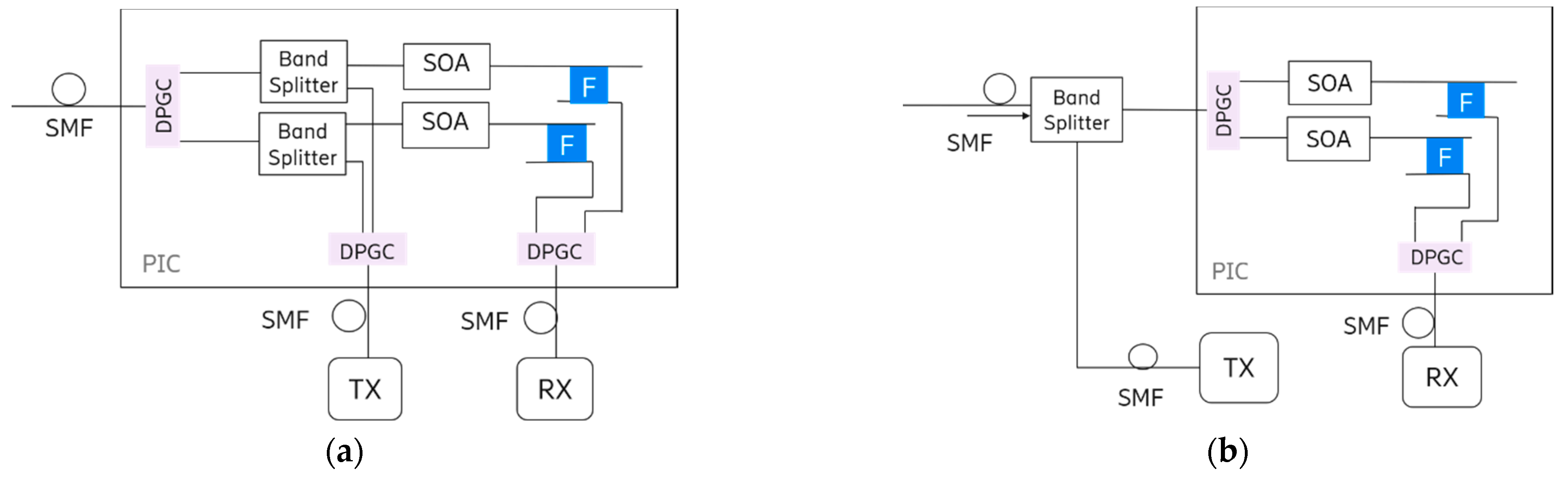
Figure 5 shows two possible architectures for a tunable transceiver including fiber coupling, a polarization diversity scheme, optical amplifiers and add and drop tunable resonators. The WDM input is split into two sub-bands that correspond to the portion of the band dedicated to the transmission channels from the transmitter (TX) and the reception channels at receiver (RX).
In this scheme the two sub-bands represent two halves of the operating BW of the transceiver. This operation can be performed by an element integrated in the photonic chip (PIC), as in
Figure 5a, or an external band splitter, as in
Figure 5b, e.g., a commercial band splitter based on thin films [
49].
The advantage of the external splitter is in the reduction in the BW that must be coupled to the photonic chip, which can represent an advantage in the fabrication of the fiber coupler. Additionally, integrated band splitters are a type of photonic element that has not yet been implemented. However, the design of integrated solutions is desirable since the use of an external band splitter might increase the footprint and consumption of the tunable transceiver.
The resonators accomplish the filtering function, adding or dropping a resonant wavelength that can be tuned, e.g., via thermo-optic variation of the refraction index of the resonator [
50]. These can be micro ring resonators (MRR), comprising multiple micro rings [
51], reflector resonators based on Bragg Gratings, such as Distributed Feedback Bragg Reflectors (DFBR) [
52] which comprise coupled Bragg gratings and a multi-mode interferometer (MMI), or ring assisted Mach–Zehnder interferometers [
53]. The requirement for these resonators is to have a free spectral range (FSR) that is larger than the operating range of the filter so to select a single wavelength within the range. This requirement is challenging for the design since it may require tight fabrication tolerances to the solutions based on micro rings, with precise control of the coupling in the add and drop waveguides [
54].
Figure 5 shows two options for the fiber-PIC coupling: the input fiber in
Figure 5a is coupled to the chip via edge coupler, whereas the output fibers in
Figure 5b are coupled via dual polarization grating couplers. The choice of the type of couplers in this architecture is determined by the bandwidth of the input and output spectrum; this is approximately 40 nm for the input coupler, therefore wide-band element, such as an edge coupler, may be preferred. On the other hand, the output couplers in this configuration operate just on one half of the BW (TX or RX) and have more relaxed constraints on the passband, that can be easily ensured by a DPGC. It must be noted that state of the art DPGC based on SiN-on-Si can presently reach a 1 dB bandwidth of at least 29 nm, with insertion losses of around 2.4 dB and 0.2 dB polarization dependent loss (PDL) [
24]. The BW can be further extended over 40 nm by exploiting a design based on SiN-on-Si platform and back mirrors as shown in [
25], where a value of 70 nm was achieved for a single polarization grating coupler. Therefore, the functional group comprising Edge Coupler (EC), Polarization Splitter (PS), and Polarization Rotator (PR) in
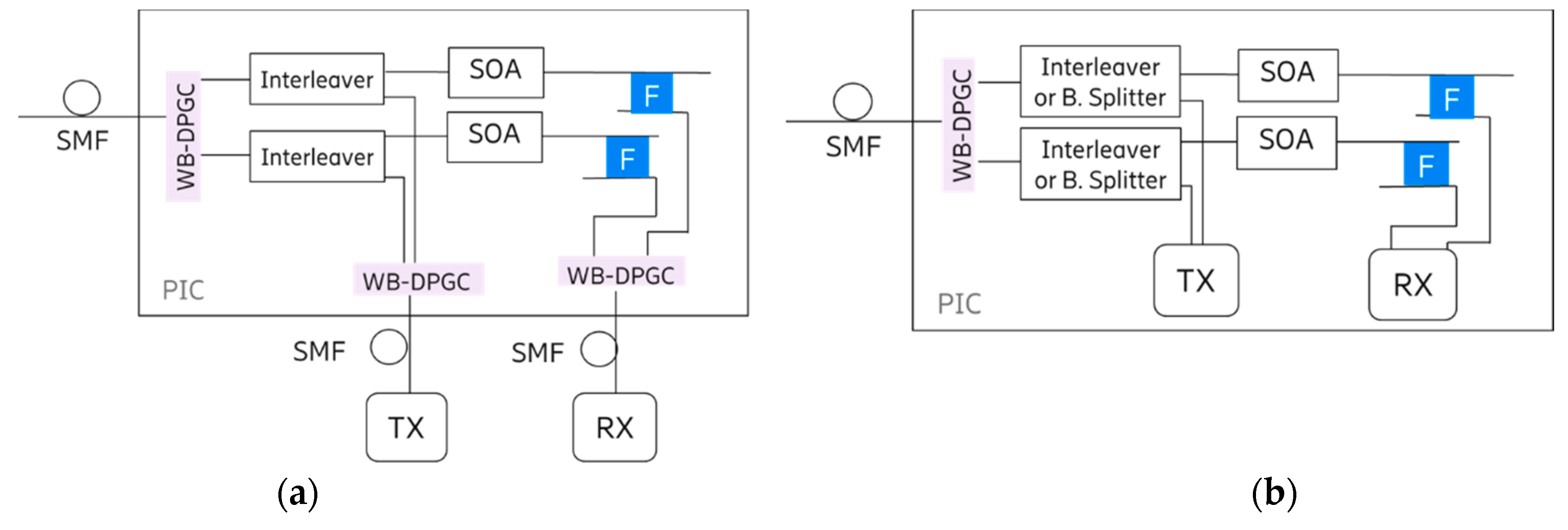
Figure 5a can be substituted with a wide bandwidth DPGC (WB-DPGC) as shown in
Figure 6.
Another design option consists in replacing the band splitter elements with solutions that operate with two interleaved sub bands. This requires an appropriate spectrum management: it is possible, e.g., to associate all odd channels to the TX and the even channels to the RX, using a filter with the appropriate FSR (equal to twice the channel spacing). This architecture solution is shown in
Figure 6a.
This kind of interleaved solutions requires both the input and the output couplers to be wideband. However, band splitters based on this scheme may consume very low power since they need minimal temperature stabilization to keep the interleaver comb filter in place.
Finally,
Figure 6b shows an architectural solution where TX and RX are integrated in the transceiver. In this architecture, laser source, modulators, and photodiode are integrated in the photonic chip and electronic divers and amplifiers can be connected to these elements through wire bonding or integrated on top of the PIC e.g., in a 3D integration scheme [
55].
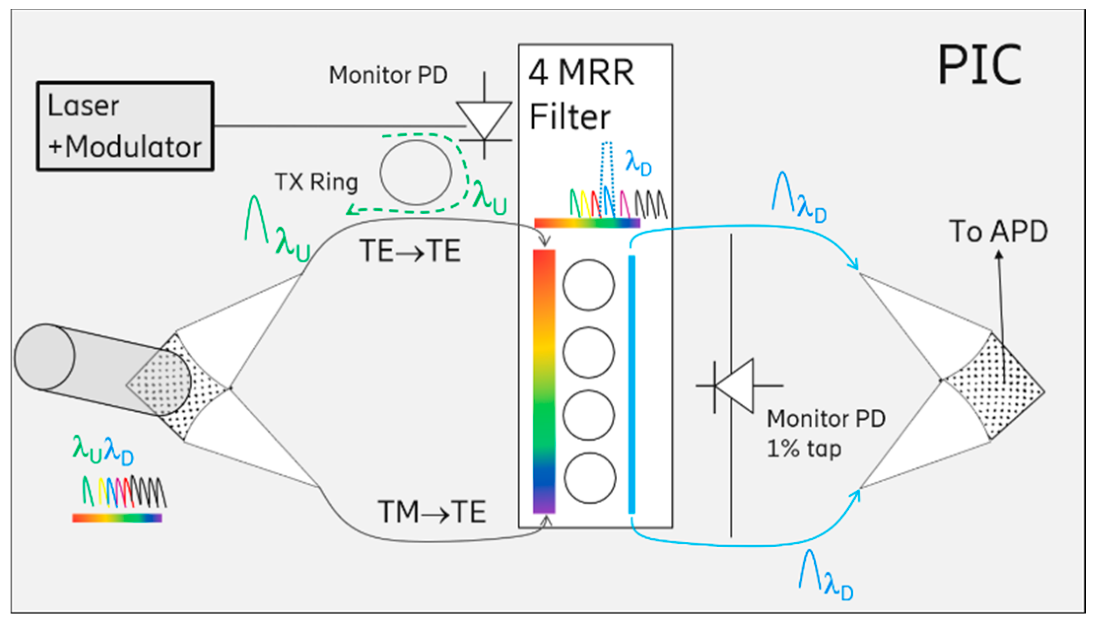
In the following, it is described a design implementation of an architecture of the type shown in
Figure 6b, which does not include the integrated SOA. The SOA can be easily integrated according to the integration process described in [
56,
57], enabling III–V integration at the backside of standard silicon photonics wafers. A detailed implementation is given in
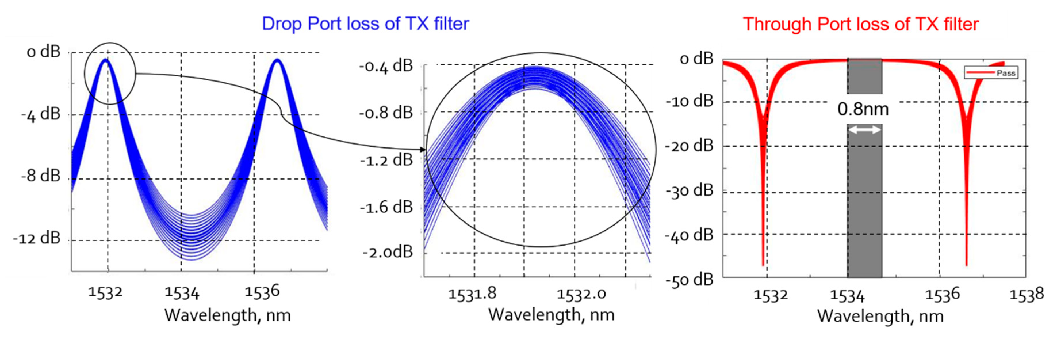
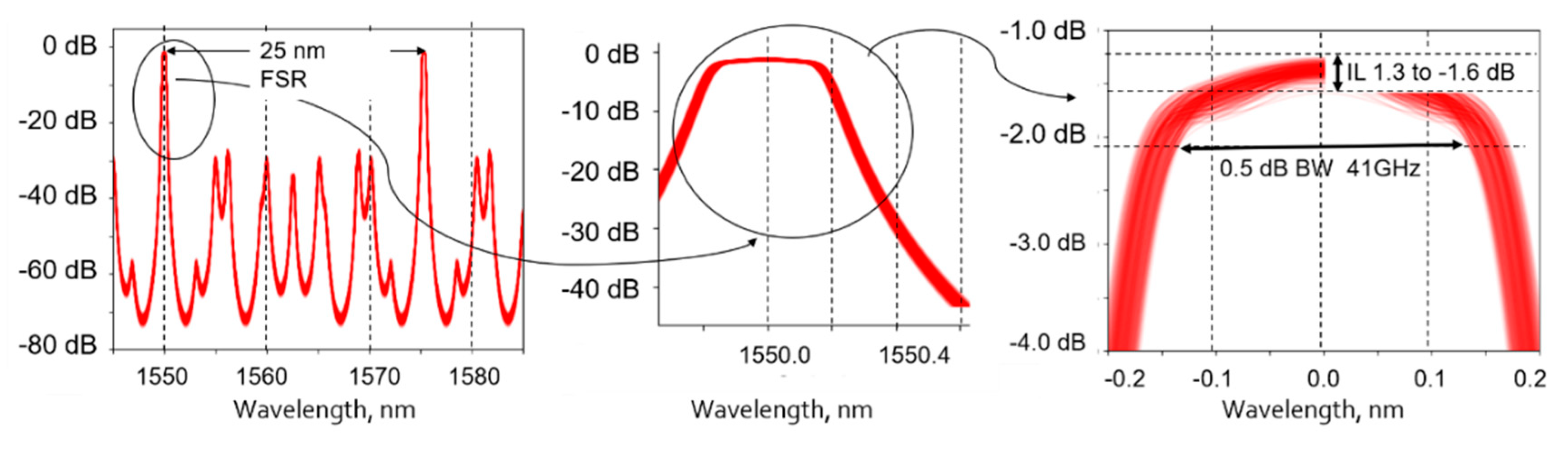
Figure 7. The filtering function at the receiver input is operated by a set of 4 coupled micro-ring resonators, whose parameters have been optimized to achieve a flat central BW of 37 GHz at −1 dB and a rejection BW of more than 25 dB. The resonator has FSR of 25 × 0.8 nm = 20 nm, corresponding to 25 WDM channels with 0.8 nm (100 GHz) spacing.
Coupling of the Photonic Integrated Circuit (PIC) with fibers is performed using surface grating couplers:
The external modulated tunable laser is fed to the chip via a Polarization Maintaining (PM) fiber, coupled with a Single Polarization Grating Coupler (SPGC) to the integrated TX ring.
The Single Mode (SM) fiber duplex, comprising the TX output and the RX input to the tunable filter is coupled to the chip via a DPGC.
The output of the RX tunable filter is coupled out from the chip to a Single Mode fiber (SMF) pigtailed with a DPGC, to reach an external avalanche photo detector (APD).
The dual polarization grating couplers separate the two orthogonal polarization components (named TE and TM in
Figure 7) of an input light into two TE polarization components propagated by two separate waveguides.
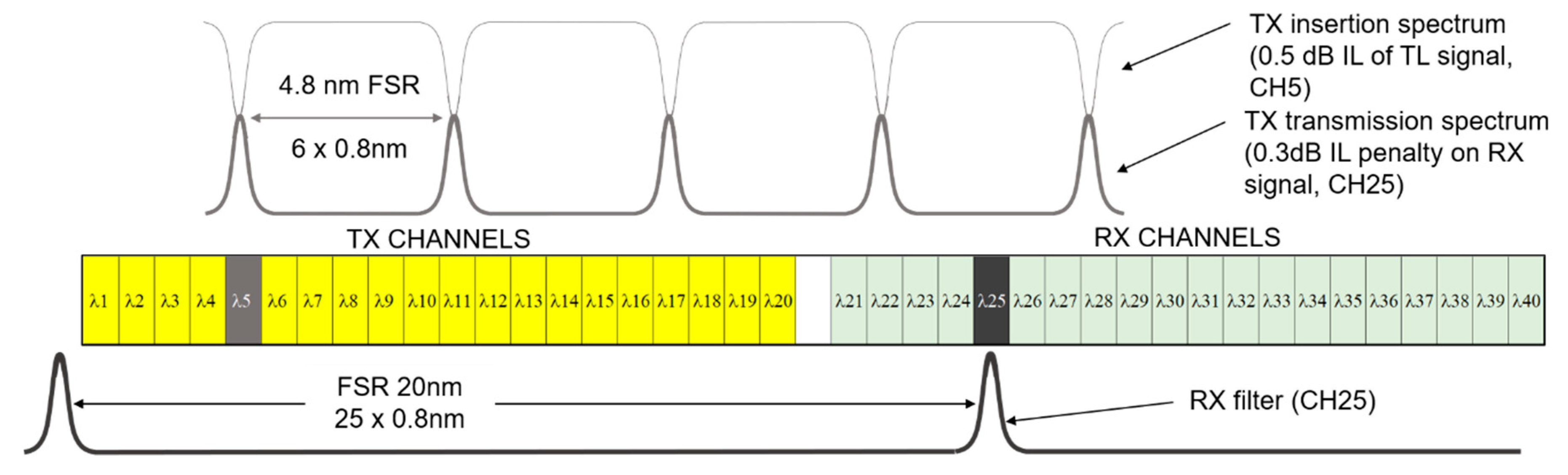
In this design, the input from the modulated external tunable laser is sent to the SM duplex fiber port via a ring filter, through the drop port (‘TX Ring’) that is tuned to the optical wavelength of the laser. The TX Ring has a FSR of 6 × 0.8 nm; this low FSR design is possible thanks to a wavelength management strategy that is implemented according to the wavelength plan described in
Figure 8. The wavelength plan comprises two groups of channels for the Uplink (UL) and the Downlink (DL): a first group of 20 T channels, from λ
1 to λ
20, are spaced by 0.8 nm on the lower C band spectrum, and a second group of twenty Rx channels, from λ
21 to λ
40, are spaced by 0.8 nm in the upper C band spectrum.
A 0.8 nm guard band, consisting in one unused channel, separates the highest TX channel λ20 from the lowest Rx channel λ21. The wavelength plan assumes that Tx and Rx wavelengths from a given Optical Network Unit (ONU), e.g., ONUi, are paired as λi/λI + 20, respectively, for the TX and RX channels (i.e., λ5 TX paired with λ25 RX, λ7 Tx paired with λ27 RX).
As shown on
Figure 8 for the case of ONU
5, when the TX filter is tuned to λ
5 for inserting the external laser, there will not be any impact on the light received at the RX, having wavelength λ
25.With such a small FSR, a large micro-ring radius of 20 μm can be used. The coupling coefficients of the rings are set to minimize the laser add loss to 0.5 dB, while the through loss seen by the RX signal on its way to the tunable receiver is kept below 0.3 dB (see
Figure 5a). When using a ring filter for adding the laser light, one should minimize the nonlinearities of the ring: this is achieved by using a low Q ring (2000) which minimizes the power within the ring.
The RX filter is more complicated as it requires to have a 20 nm FSR. A single ring cannot be used due to the flatness requirements, BW and extinction specifications; the design is based on 4 coupled rings.
For the realization of both TX and RX filters, one needs to consider the dispersions that characterize the fabrication process. The Silicon on Insulator (SOI) thickness variation (±10 % of the SOI thickness) accounts the most in the ring performances variations. This adds on to the width variation of the waveguides.
Figure 9 and
Figure 10 show the range of performance variation calculated via Monte Carlo (MC) simulations for each filter, assuming a dispersion in the coupling coefficients of ±10%. These assumptions were verified in a first fabrication run with a set of rings with different coupling coefficients.
The estimated footprint for the photonic chip comprising filters, couplers and additional monitor photodiodes is 2.5 × 3.7 mm, where the RX (APD and amplifiers) and TX (modulators and tunable laser) are external.
5. ROADM in Silicon Photonics
As reported in
Section 2, low cost, reduced size ROADMs are a key technology for providing the right level of automation in the access network segment. Tunable filters can be used to operate the wavelength selection in a ROADM [
58]. When used in ROADMs, tunable optical filters relieve operators from deploying and storing many variants of fixed optical add drop multiplexers (OADM) where each fixed OADM corresponds to a specific group of wavelengths by replacing the fixed OADMs with a single reconfigurable device. This leads to advantages in network planning simplification and saving of costs for the acquisition and maintenance of backup components, which are necessary to cope with possible failures, as failures can be addressed with a single tunable device.
Different WSS technologies exist, based on Microelectromechanical Mirrors (MEMS), Liquid Crystal (LC) on glass and Liquid Crystal on Silicon (LCoS) [
59,
60]. LCoS technology dominates current WSS shipments because it can support flexible channel plans. However, LCoS devices are polarization dependent, they need a polarization diversity configuration. Additionally, cost, size, port isolation, and crosstalk remain major design challenges. ROADMs architectures based on WSS, that reduce cost and fiber connections, with respect to traditional solutions, are reported in [
61]. However, they are far to meet the requirements of the network scenarios presented in
Section 2, for which a truly low-cost ROADM node is essential.
Silicon photonics are the best candidates for such networks due to its characteristics of easy integration with control electronics, miniaturization, mass producibility, and potential for high yield and low cost in the well-established CMOS production infrastructure. In [
1,
25,
62] examples of system-on-chip ROADMs, referred as Mini-ROADM, are presented. An example of architecture for the Mini-ROADM is depicted in
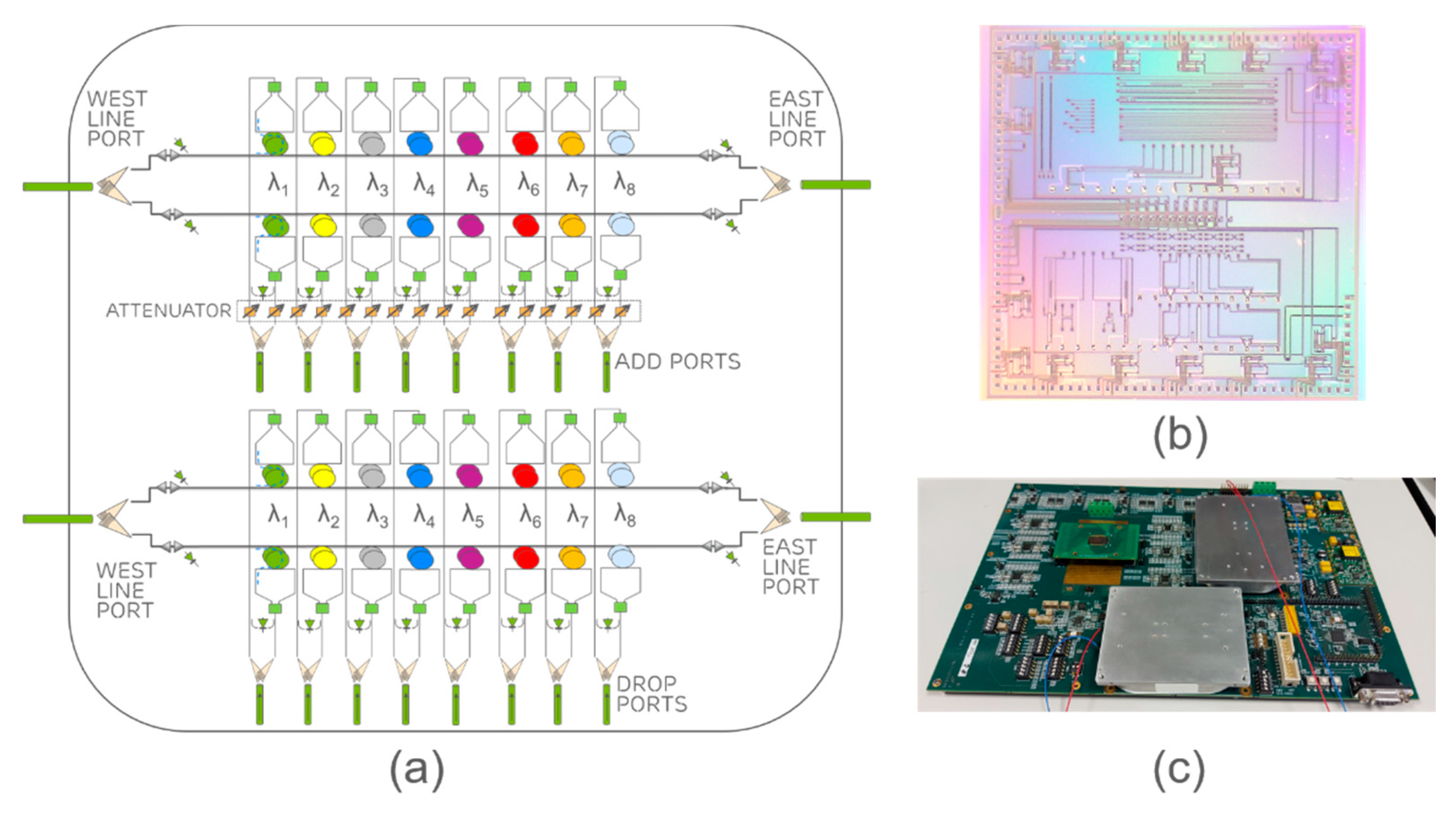
Figure 11.
This device has two-line ports, referred as east and west line port, for operation over two fibers rings. It presents two independent structures, one used for adding WDM channels to send the output line port, and the other used for dropping channels from the input line port. In a prototype realized at Ericsson Research, each structure comprises 8 ports to add and drop an equal number of 200 GHz spaced WDM channels in C band. A similar design can be generalized to a higher number of 100 GHz spaced channels. Such a two-way Mini-ROADM can be also enhanced to operate over a larger number of ways: for instance, a 4-way ROADM can be realized by connecting 4 of these structures [
63]. In the Mini-ROADM, optical channels are added and dropped by silicon micro-ring resonators (MRR) as wavelength-selective switching elements that also acts as an optical filter.
Each wavelength switching element is implemented by two-coupled MRRs with a slight resonance offset, set to obtain 40 GHz optical BW at −1 dB. The measured adjacent channel isolation is larger than 20 dB.
Silicon photonics MRRoptical filters have multiple advantages respect to other types of filter technologies since they are low cost, have low power consumption, and have a very small footprint in the range of micrometers. However, they are resonant devices, quite sensitive to temperature variations, and for operating correctly in the system the wavelength resonance needs to be stabilized.
Two possible methods can be adopted for MRR resonance stabilization:
Use of a temperature control circuit to keep the temperature of the entire PIC at a pre-determined value by using an off-chip thermo-electric cooler (TEC). The TEC is used as the actuator that is driven by a feedback control (usually a PID), together with an integrated temperature sensor
Use of an active tuning circuit to lock the MRR resonance to the carrier wavelength by using a micro-heater as actuator on top of the MRR.
Method (1) has the advantage of requiring electronic circuits with limited complexity but it requires more power to stabilize the whole PIC temperature.
Method (2) requires control circuits with higher complexity, with respect to approach (1), but has the advantage of requiring very low power, of the order of few mWatt per MRR. Additionally, the package is simplified by the absence of the TEC.
In the design of the mini-ROADM the approach (1) was preferred for its implementation simplicity. The temperature stabilization circuit required 1–2 W power to provide an accuracy of 0.1 C and a response time of the order of 1 ms.
Each structure in the mini-ROADM has a polarization diversity architecture, with a double-polarization grating coupler at the input that adapts the random polarization of the input signal to the device’s main propagation mode. At the output ports, the two polarization components are recombined before coupling to the optical fibers. A previous version of this device was realized with a single polarization, as it was made insensitive to the input polarization with an integrated polarization controller [
62,
63]. However, with a single polarization controller the operation requires a low PMD, since different WDM channels, though launched with equal polarization, arrive with random polarization alignment at the input like port. Therefore, a dual polarization architecture is preferred.
The PIC of the mini-ROADM prototype has a size of 5 × 5 mm (see
Figure 11b). The PIC is mounted on a control board (see
Figure 11c) to provide functionalities, such as the adjustment of MRR heater currents for performing channel add or drop, and setting the propagation direction of each individual wavelength at the 1 × 2 switch placed at the add port (
Figure 11a). Each switch reverts the propagation direction, e.g., for traffic protection in case of fiber break. This allows to implement well-known ring protection mechanisms without duplication of the optical interfaces at each add or drop port.
The control board is equipped with two Erbium Doped Fiber Amplifiers (EDFA) with a gain of 23 dB and maximum output power of 20 dBm, one for each bus in function of the working direction of the wavelengths along the network. The high gain and output power compensate the high coupling loss of the prototype, due to the non-ideal grating coupler fabrication process. They can be considerably lower in an engineered device. Integrated SOAs can be also considered but they have the limitations discussed in
Section 2.
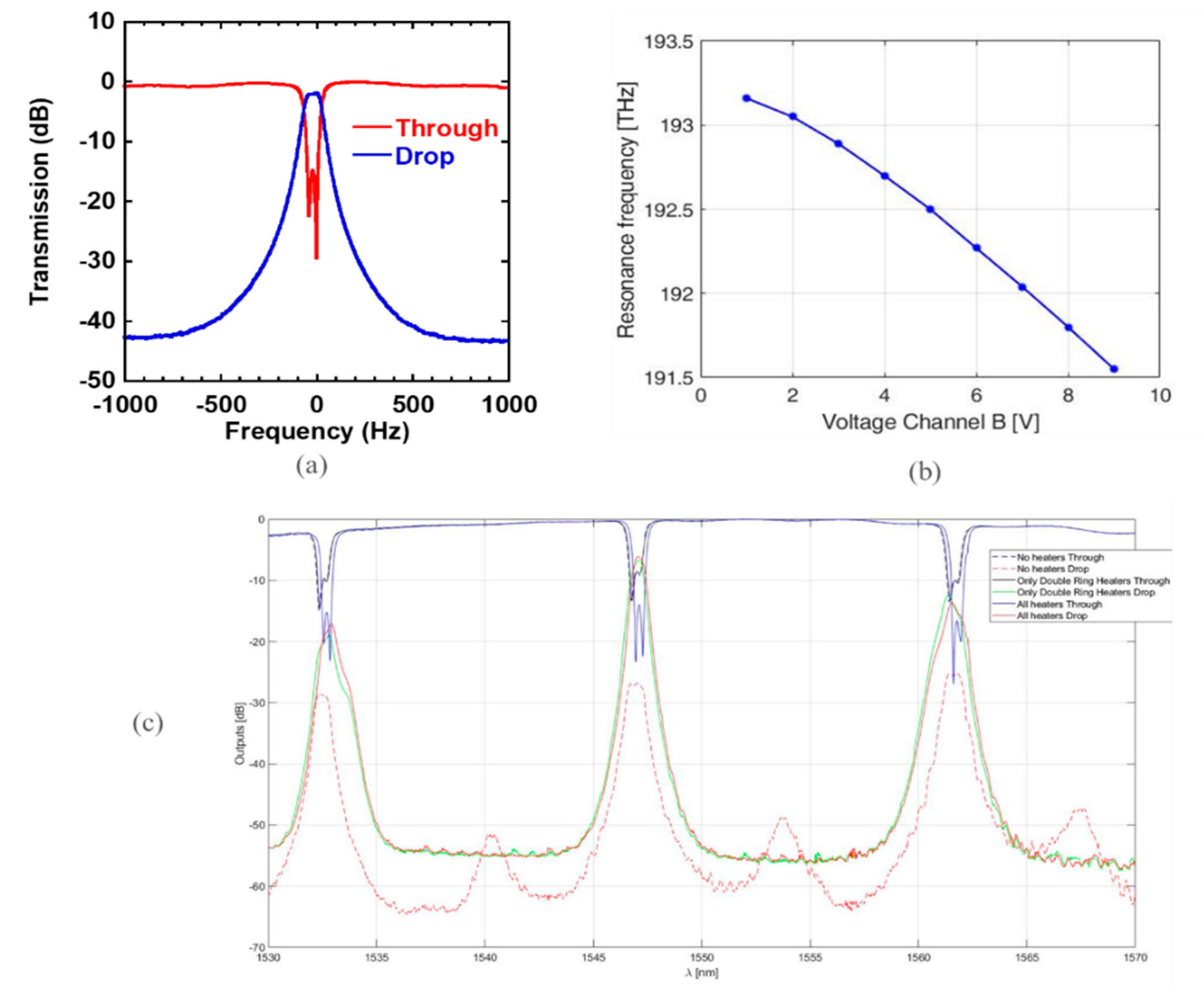
The spectrum of one the MRR is shown in
Figure 12a, for a channel passing through the MRR and a dropped channel. The measured drop loss is 1.8 dB, excluding the polarization grating coupler losses. The maximum drop loss difference from the first to the last channels is about 1.5 dB.
The resonance frequency is plotted in
Figure 12b versus different voltage values applied on the MRR heater. The curve in
Figure 12b shows that the efficiency of tunability is 35 µW/GHz.
In
Figure 12c is shown the spectral output of a single channel in three different operating conditions: (i) all heaters are switched off (‘no heaters through/drop’ in the legend) (ii) only the channel heaters are enabled, all the other channels are switched off (‘only double ring heaters through/drop’ in the legend); and (iii) both the channels heaters and all the other channels heaters are enabled (‘all heaters through/drop’ in the legend).
With the current silicon photonics technology, it is possible to expand the number of WDM channels up to 24 but supporting denser frequency spacing (e.g., 50 GHz) would require technological advances to improve the wavelength stability of the micro-rings.
As final remark, optical attenuators can also be integrated at the input of the add channel ports to adjust the transmitted optical power so that the WDM channels are equalized at the line output port (attenuators shown in
Figure 5 but not implemented in the prototype discussed here). This would allow to avoid big power mismatch between bypass signals and added signals, and related crosstalk issues.


