Article

Machine Learning Based Energy-Efficient Design Approach for Interconnects in Circuits and Systems

College of Information and Communication Engineering, Sungkyunkwan University, Suwon 16419, Korea
*
Author to whom correspondence should be addressed.
Appl. Sci. 2021, 11(3), 915; https://doi.org/10.3390/app11030915
Submission received: 31 December 2020 / Revised: 18 January 2021 / Accepted: 18 January 2021 / Published: 20 January 2021
(This article belongs to the Special Issue Emerging Mobile Computing Technology: Ultra-high Energy Efficiency)

Abstract

:
In this paper, we propose an efficient design methodology for energy-efficient off-chip interconnect. This approach leverages an artificial neural network (ANN) as a surrogate model that significantly improves design efficiency in the frequency-domain. This model utilizes design specifications as the constraint functions to guarantee the satisfaction of design requirements. Additionally, a specified objective function to select low-loss and low-noise structure is employed to determine the optimal case from a large design space. The proposed design flow can find the optimum design that gives maximum eye height (EH) with the largest allowable transmitter supply voltage ( V T X ) reduction for minimum power consumption. The proposed approach is applied to the microstrip line and stripline structures with single-ended and differential signals for general applicability. For the microstrip line, the proposed methodology performs at a performance speed with 42.7 and 0.5 s per structure for the data generation and optimization process, respectively. In addition, the optimal microstrip line design achieves a 25% V T X reduction. In stripline structures, it takes 31.9 s for the data generation and 0.6 s for the optimization process per structure when the power efficiency reaches a maximum 30.7% peak to peak V T X decrease.

1. Introduction

The emergence of the Internet of Things (IoT) demands low-power circuits to perform on-device data processing [
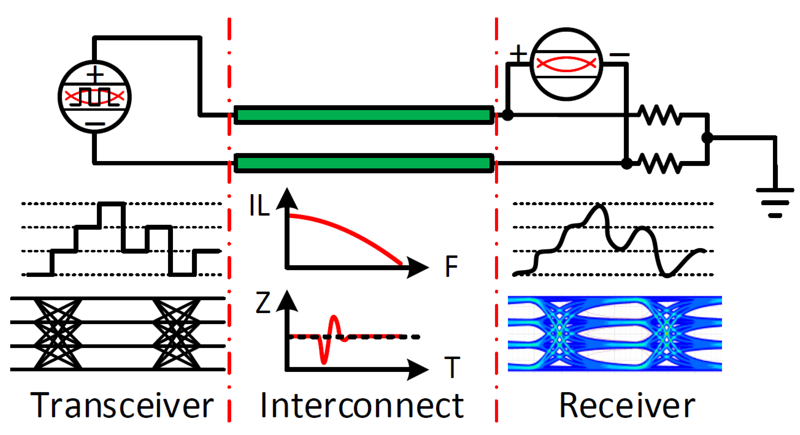
1]. Hence, the IoT applications expect energy-efficient solutions at all design levels. On the hardware level, the interconnect acts as the communication channel between circuits that also consumes power. A typical data transmission that system includes driver, receiver, and interconnect is shown in Figure 1 below.
While most effort has been concentrated on the on-chip circuit and interconnects’ optimization [2,3,4,5,6,7,8], the energy-aware off-chip interconnect optimization in the transceiver circuit has not been investigated thoroughly so far [9,10]. The authors in [2,3,4] focused on energy-efficient on-chip interconnect design. The approach in [2] lessens power consumption based on an adaptive voltage scheme while the authors in [3,4] proposed a design framework that models and optimizes the energy-efficient on-chip interconnect. On the other hand, authors in [5,6,7,8] attempt to reduce power consumption by advanced circuit techniques. While the authors in [5,6] diminish the power consumption by an efficient pre-emphasis transmitter, the proposed approach in [7] minimizes the power consumption by reducing voltage swing with a low-power forward error correction architecture. The authors in [8] suggest power analysis and optimization by trading off transmitter voltage swing and receiver gain.
These works mentioned above attempt to reduce the transmitter voltage swing without considering its impact on the interconnect leading to two main drawbacks. Firstly, the interconnect has parasitic resistance and capacitance which play a significant role in power dissipation. Secondly, voltage swing reduction at the transmitter due to the signal loss and crosstalk always degrades the receiver signal quality at the receiver. On the other hand, the authors in [9,10] are concerned with energy-efficiency evaluation for the off-chip interconnect, while the approach in [9] proposes an energy-aware analysis with analytical formulas using frequency-domain information. The authors in [10] provide a more comprehensive methodology to evaluate the energy efficiency of the I/O links. However, these works with the conventional design procedure lack an efficient methodology to investigate the immense design space thoroughly. Although the channel in these works is efficiently modeled by analytical approaches proposed in [11,12], these approaches have difficulties modeling the complicated structures.
The hardware design procedure including the interconnect design is an iterative process in a human manner. Recently, the rise of machine learning techniques exhibits the hope for an efficient design approach. Hence, many works focus on applying machine learning techniques to improve design efficiency. The approach in [13] proposes a fast and accurate high-speed channel modeling using an artificial neural network (ANN). Moreover, the genetic algorithm (GA) is utilized to optimize the design. However, this work employs the W-element model for the lossy multi-conductor extracted from the 2-D EM simulator. Hence, it may be inapplicable to the complex structure that requires 3-D EM simulation. Alternatively, the proposed approach in [14] predicts eye height and eye width based on the ANN model trained by S-parameter in frequency-domain. This approach provides a fast alternative solution in the time-domain. An extension of this approach in [15] illustrates general applicability with complex numerical examples. Furthermore, the authors in [15] demonstrates the superior of ANN by a comprehensive comparison. The authors in [16] enhance the ANN model performance in [15] with feature selection algorithms described in [17,18]. On the other hand, the authors in [19] use the ANN model to model crosstalk in high-speed transmission lines. However, this approach requires both frequency-domain and time-domain simulation to generate training data for the ANN leading to inefficiency in a complex structure. These approaches require both frequency-domain and time-domain simulation to acquire the training data. Although the ANN model can directly predict the time-domain parameters, both frequency-domain and time-domain simulations in these approaches consume significant effort. Additionally, the frequency-domain is the most time-consuming stage in the design procedure. Moreover, it is a crucial task to analyze and optimize the channel properties in this domain.
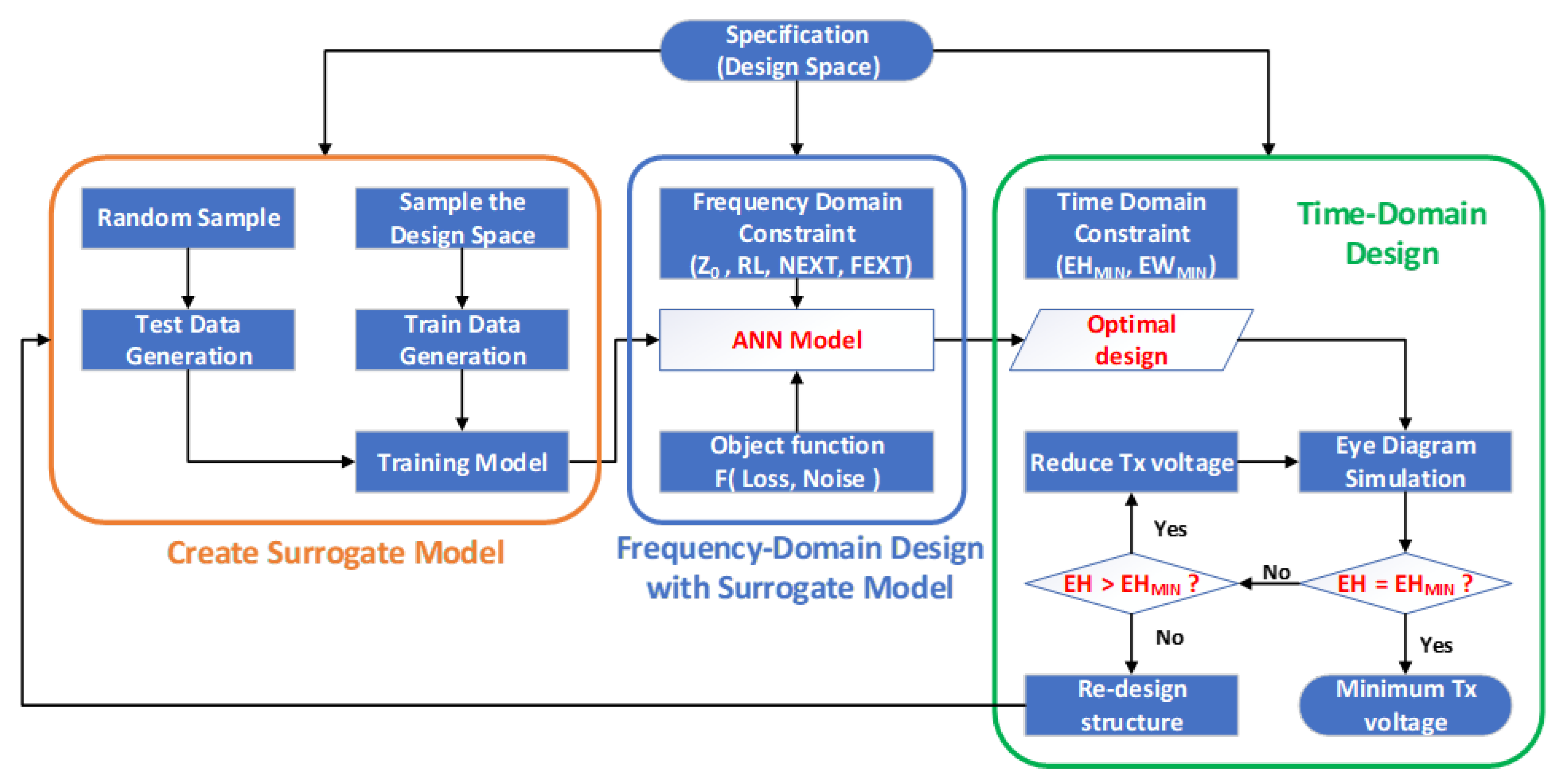
Hence, this paper proposes a low-power design methodology based on ANN to overcome these shortcomings. The proposed methodology leverages the ANN model to produce reliable data in the frequency-domain quickly. This model significantly improves the design efficiency in the frequency-domain. In addition, the method utilizes the ANN model to determine the optimal structure with the objective function. The optimal structure and condition that are found from the proposed approach provides the highest margin in the eye diagram for transmitter supply voltage reduction. Hence, the designer can reduce the voltage swing at the transmitter circuit while the signal quality is still guaranteed.
The rest of the paper is organized as follows: Section 2 describes the important parameters in the printed circuit board (PCB) interconnect design. Subsequently, Section 3 introduces the artificial neural network and the proposed approach. Following that, Section 4 illustrates the approach efficiency in typical structures including microstrip line and stripline. Finally, Section 5 summarizes the conclusions about the applicability of the proposed approach.

2. Low Power Approach for Interconnect Design

2.1. Off-Chip Interconnect Design Flow

Designing a transmission line for off-chip interconnect is a multi-dimensional process. The design procedure of a transmission line includes both the frequency domain and the time domain due to the its frequency-dependent characteristics. While the scattering parameter (S-parameter) is typically employed to evaluate design properties in the frequency domain, the eye diagram with eye height (EH) and eye width (EW) is generally used to determine the signal quality in the time domain. Additionally, the characteristic impedance ( Z 0 ), which is a significant parameter, is required to design carefully to avoid reflection loss along the interconnect.

2.1.1. Frequency Domain Design

According to circuit theory, the lumped model is employed to represent circuit components with neglecting propagation time. At a higher frequency, the propagation time in the interconnect is considerable in comparison to the signal period. Hence, the lumped model is insufficient to describe the structure. In this case, the interconnect is the transmission line modeled by the distributed model. In transmission lines, voltages and currents are expressed as wave propagation along the line. Moreover, the characteristic impedance ( Z 0 ) of the transmission line is defined as the ratio of voltage and current wave propagation along the line [20]. Alternatively, the characteristic impedance is also a function of the R, L, G, C parameters of the transmission line, which are frequency-dependent. Thus, this characteristic impedance is also a frequency-dependent parameter. Theoretically, this impedance is constant along the length of the transmission line at a specific frequency. However, the system includes not only the transmission line but also other connectors such as vias, SMA, and so on. Hence, the mismatch impedance between these components results in reflection loss. As a consequence, the impedance is one of the most significant parameters in the interconnect design that typically is 50 Ω for a single-ended signal and 100 Ω for a differential signal.
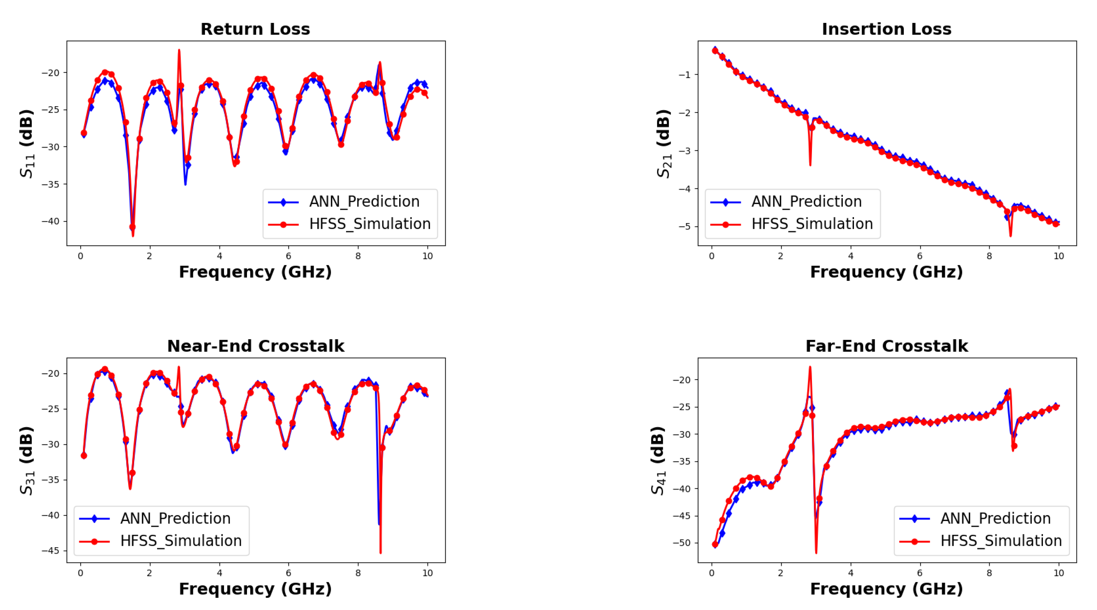
In addition to the characteristic impedance, the values of scattering parameters (S-parameters) need to be investigated carefully in the design procedure. Typically, an N-port network is employed to represent the network at high frequency. The concept of equivalent voltages and current and the related impedance and admittance matrices are developed to describe the network. However, these concepts become abstract when dealing with the high-frequency network. Thus, the scattering matrix is preferable to provide a complete description of an N-port network. While the characteristic impedance represents the ratio between voltage and current wave in the transmission line, the S-parameters express the relationship between the incident and reflected voltage in the N-port network [20]. In the N-port, a specific parameter S i j is determined as below
S i j = V i V + j w i t h V + k = 0 f o r k j
where:
Vi:
 Reflected voltage from port i
V+j:
 Incident voltage at port j
The S-parameters of a four-port network show all the significant parameters of two coupled interconnects. S 21 represents the insertion loss throughout the channel including material, conductor, and radiation loss. The reflection loss caused by the mismatch impedance is represented in S 11 . Additionally, the crosstalk comprised of near-end crosstalk (NEXT) and far-end crosstalk (FEXT) is represented by S 31 and S 41 , respectively.

2.1.2. Design in Time Domain

Although Z 0 and S-parameters characterized in the frequency domain represent many of the significant performance parameters in the frequency domain, the ultimate figure of merit to evaluate the channel is the eye diagram that belongs to time-domain design. The eye diagram is a statistical convolution of multiple signals at the receiver that forms a figure similar to the eye. The EH and EW are employed to evaluate the quality of the signal arriving at the receiver. However, the frequency domain information is applied to obtain the eye diagram at the receiver. As a consequence, the interconnect design requires both frequency domain and time domain. The conventional flow is shown in Figure 2 below.

2.2. Low Power Approach for Interconnect Design

According to the proposed approach in [10], an equivalent circuit with analytical formulas is inferred to evaluate the power performance. In this approach, the power dissipation is directly proportional to the transmitter supply voltage and the input impedance is a function of the interconnect characteristics and termination impedance. While the interconnect characteristics are frequency-dependent, the termination impedance comprises the transmitter output impedance and the receiver input impedance. The termination impedance is generally similar to the channel characteristic impedance to avoid reflection. This impedance value is typically 50 Ω for the single-ended signal and 100 Ω for the differential signal. As a result, the interconnect and the transmitter supply voltage are the controllable parameters for low-power interconnect design.
The power consumption of transceiver system is mainly from the switching activity of the circuits and the leakage current from transistors. This power is directly supplied by the voltage source. Therefore, in addition to reducing the leakage current and switching actions, reducing the voltage source is an efficient method for power saving in which the power is a trade-off with the speeds. Thus, many efforts concentrate on reducing the transmitter supply voltage by advanced circuit techniques. However, a decrease in transmitter voltage swing without considering the interconnect results in unreliable function. This reduction will harm the transmitter signal quality and make it more sensitive to noise along the interconnect. Hence, this voltage reduction degrades the signal to noise ratio (SNR) and this may lead to an inapplicable in transceiver system. Because the interconnect deals with signal transmission, the power consumption throughout the channel is not provided by the voltage source supply. This power directly accounts for the input power leading to worsened signal quality at the receiver determined by the EH and EW. The power consumption in the interconnect comes from the loss throughout the channel including insertion loss, return loss, and noise. Consequently, saving the power-consumption in the interconnect is equivalent to minimizing the channel loss. Thus, the low-power interconnect design has the trade-off relation between performance and power. Therefore, an optimized interconnect should be designed for better power efficiency. As a consequence, it can be applied to design the low-power system without impacting the signal quality.
In addition to the channel loss, the crosstalk also plays a vital role in the design procedure. The induced noise voltage produced by crosstalk can degrade the signal quality at the receiver. However, this signal is proportional to the transmitter supply voltage. Hence, eliminating this noise increases the transmitter supply voltage resulting in additional power consumption. As a consequence, the design procedure contains crosstalk analysis to deliver a low-power structure. In conclusion, the optimal low-power interconnect is a low-loss and low-noise structure that can operate at low transmitter supply voltage with acceptable signal quality.

3. ANN-Based Design Methodology for Low-Power Interconnect

3.1. Limitations in Frequency Domain Design

The characteristics of the eye diagram determine the signal quality in the time-domain simulation. However, this simulation requires the information of channel properties from the frequency-domain. In the conventional design procedure, the frequency-domain design is also the most time-consuming stage due to the iteration simulations to find the optimal structure. Moreover, it also requires lots of effort in analysis to ensure design optimization. Furthermore, technology development grows the complexity of design with the increase in the number of design parameters. This complexity requires not only more simulations but also exceeds the analysis ability of the designer. While the time-consuming simulation expects an alternative method to minimize the design cycle, the optimization procedure demands an analytical approach to achieve the optimal design. Therefore, a surrogate model that quickly generates accurate data is essential to reduce the design time. Furthermore, an objective function utilizes this model to assure the design optimization for low-power applications.

3.2. Artificial Neural Network (ANN)

An Artificial Neural Network (ANN) inspired by the neural network in a person’s brain attempts to simplify and mimic our brain behavior. The ANN can be trained in a supervised or unsupervised manner. In this design methodology, a supervised learning ANN model trained by given data predicts the interconnect properties. In this kind of learning, the ANN model can deliver high accuracy prediction by providing enough training data and employing appropriate data processing techniques. The activation function stimulates the biological neuron in ANN. These neurons form a hierarchy network referred to as multiple layers in which the output of some neurons is input to others. Each neuron called a node takes multiple weighted inputs (w), bias (b) applied the activation function (f) to the summation of these inputs, and in doing so generates an output (H). The general form of the activation function is described in Equation (2). The neuron and the ANN model are shown in Figure 3 and Figure 4, respectively.
H ( w , b ) = f ( x × w + b )
In the supervised learning ANN, the idea is to reduce the error between the input and the desired output. The training procedure to minimize this error has a significant impact on the ANN performance. This process is strongly influenced by the training algorithm such as Gradient Descent or the backpropagation method. While the Gradient Descent uses the gradient of the error function to make an informed step-change in weight (w) to achieve minimum error, the backpropagation allows the ANN to determine the impact of one specific weight on errors by calculating the partial derivatives. This training process is an iterative method that involves multiple steps.

3.3. Proposed Design Methodology

In this approach, a surrogate model based on ANN is generated using the design requirements. The model serves as a fast and high-accuracy data generation tool in frequency-domain designs. In addition, the objective function and design constraints aid this model to deliver the optimal structure. Finally, the minimum allowable transmitter supply voltage for maximum power saving is determined in time-domain design. The proposed design methodology is illustrated in Figure 5.

3.3.1. The Surrogate Model Based on ANN

The interconnect design contains two essential kinds of parameters related to the structure and the materials. The structure parameters are comprised of the physical dimensions determine the design geometry and are limited only by the area and fabrication technology. Conversely, design materials presenting the properties of dielectric and metal are typically constant during the design process. Hence, the structure dimensions such as width, space are the input of the ANN model. Additionally, the frequency is one of the model inputs due to the frequency-dependent feature. Moreover, the channel properties in the frequency domain including S-parameter and Z 0 are the model output. The output data included S-parameter and Z 0 are produced by simulating structures with full-wave simulations HFSS and Q2D, respectively [21]. In this approach, a surrogate model based ANN is employed to speed up the frequency domain design procedure. In the training phase, the ANN model maps the output and input through the given training data. These data are randomized before training and is divided into training data and testing data with a ratio of 80% and 20%, respectively. While the training data directly provide information to the model, the testing data is employed to track the prediction accuracy during the training process. Furthermore, the validation data are utilized to ensure the model accuracy after it is established. Finally, an ANN model that quickly provides accurate frequency-dependent characteristics of any design structure is created.
The performance metric is defined to evaluate the ANN prediction performance. In this design methodology, the goal is to predict the interconnect properties included the S-parameter and Z 0 of a specific frequency range. Thus, we use residual (R) and root mean square error (RMSE) as the fundamental metrics to evaluate prediction performance.
The residual from a fitted model is defined as the differences between the predicted data and real data at each predictor value. On the other hand, root mean square error (RMSE) that measures the average of the square of the errors is also a performance metric that we considered. In addition, error in terms of percentage is considered for the reference purpose only because it relies on the real data that can be very small. In this case, the slight difference in prediction can cause a high error in terms of percentage. The residual, RMSE, and error are described in Equations (3)–(5), respectively.
R = Y Y
R M S E = 1 N i = 1 N ( Y Y ) 2
E r r o r = 1 N i = 1 N | Y Y | | Y | 100
where:
Y:
 the actual value
Y’:
 the prediction value
N:
 the number of frequency points

3.3.2. Design in Frequency Domain

In the frequency domain design, the surrogate model is leveraged to provide data for the analysis and the optimization procedure. Intuitively, the ANN model is a combination of math equations considered a black-box function that maps the input and output. Hence, the objective function assists this model in attaining the optimal structure instantly. Moreover, the optimization procedure is automated to avoid human error. Additionally, the specifications including characteristic impedance, return loss, and crosstalk are the constraints to find the optimal structure.
Two primary factors that degrade the signal propagated throughout the channel are loss and noise. While the insertion loss S 21 presents the channel loss included the dielectric and material loss, the crosstalk corresponds with the noise caused by the adjacent channel. Although both S 31 and S 41 are crosstalk noise, the near-end crosstalk S 31 flows toward the transmitter and has no impact on the receiver signal. Conversely, the far-end crosstalk S 41 plays a significant role in the receiver signal by boosting or degrading the eye diagram. The FEXT coefficient described in Equation (6) is a function of channel length, the coupling difference, propagation velocity, and the transition time [22]. Thus, a general strategy for defining the objective function used in this paper is to find the best case at the receiver after suffering both insertion loss and crosstalk.
F E X T = 1 2 × L v p × t r i s e × ( C M C S L M L S )
where:
L:
   Channel length
vp:
   Propagation velocity
trise:
   Transition time
CM,CS:
 Mutual and self capacitance, respectively
LM,LS:
 Mutual and self inductance, respectively

3.3.3. Time-Domain Optimization

The time-domain simulation is performed with the optimal structure observed in the frequency domain. The EH and the EW presented for the eye-opening determine the quality of the signal in this simulation. While the EW is sensitive to the jitter and the signal transition, the EH is directly proportional to the signal amplitude at a specific frequency. Hence, the reduction in voltage to save power will degrade the EH that harms the signal integrity, and can not meet the design requirements. Thus, the optimal design that gives maximum EH provides the designer with the highest margin to minimize the transmitter supply voltage satisfying the minimum EH requirement. Consequently, the power consumption is minimized with the minimum allowable voltage estimated by the following Equation (7).
V T X , M I N = V S U P P L Y E H M A X E H M I N
where:
VTX,MIN:
 Minimum allowable transmitter supply voltage
VSUPPLY:
 The supply voltage in design conditions
EHMAX:
  Maximum eye height
EHMIN:
   Minimum eye height in design conditions

4. Analysis Results

In this section, the proposed design procedure is applied to two typical structures in the interconnect design. The first example is a microstrip line structure using the single-end signal and the second one is a stripline structure employing the differential signal. The computer configuration of 128 GB Memory, Intel Core i7-9800X CPU, and NVIDIA GeForce RTX 2070 Super GPU was used to perform the simulation. The design details are illustrated in the following sections.

4.1. Single-Ended Microstrip Line

4.1.1. Design Structure

In the interconnect design, the microstrip line is one of the most typical structures due to the simplicity in design and fabrication. However, it takes a lot of time to design and optimize this structure. This structure constitutes one dielectric layer and two metal layers comprised of a ground plane and the signal layer. The signal layer contains one or multiple parallel buses with the channel width (W) plus the distance between them (D) referred to as the physical dimensions. The ratio ( K D ) between the space and width is typically about 2–3 to minimize crosstalk. However, the cost is the expansion of the area. They are the main parameters to determine the channel characteristics. The dielectric properties including its height (H) plus the dielectric constant have a significant impact on the channel. The structure geometry is shown in Figure 6.

4.1.2. ANN Model and Optimal Structure in Frequency Domain

In this design, the essential parameters of the structure are ANN model inputs. The space ratio K D shown in Figure 6 is used as a model input instead of the absolute distance. Hence, the ANN model inputs are the W, K D , and frequency. The constraint of physical dimensions is evenly sampled to produce the training data in which each data set depicts the structure properties over the range of interest frequency from 0.1 GHz to 10 GHz with a step size of 0.1 GHz. Moreover, both S-parameter and Z 0 are the model output. The validation data are generated to examine the accuracy of the ANN model. The channel length of 50 mm and FR4 with dielectric thickness of 20 μm with relative permittivity of 4.4 are used in this design. The minimum EH requirement at a 10 GHz data rate is 250 mV with a 1 V transmitter supply voltage ( V T X ). Table 1 below shows a summary of the training and validation data.
A sampling design space with W of 5 μm for W and K D of 0.1 consists of 496 structures. To generate 28 data sets for training data and validation, it takes 700.8 s per structure. The training process to construct the ANN model takes 1468.9 s. The optimization in the frequency domain takes 248 s to determine the optimal design among 496 structures. The proposed modeling and optimization flow takes a total of only 43.2 s to come up with the optimum design which includes 42.7 s for data generation and 0.5 s for optimization. Hence, the proposed approach is much more efficient than the traditional manual design methods. The accuracy of the ANN model with respect to the validation test data is summarized in Table 2. The errors of S 21 and Z 0 are 0.11 dB and 0.45 Ω , respectively, which proves that the ANN model is highly accurate. The residual errors of S 11 , S 31 , and S 41 are small with values of 0.97 dB, 1.63 dB, and 1.17 dB, respectively. All parameters prediction performs a percentage error below 5%; one of the return loss is a bit higher with 6.73%. However, this higher error is mainly from the resonance points in the return loss and had a small effect on the design. Hence, the ANN model is reliable to predict the optimal structure.
The optimal structure needs to satisfy the specifications included characteristic impedance, return loss, and the crosstalk level. Hence, Z 0 of 40–60 Ω and a maximum S 11 of −15 dB are the design constraints. Furthermore, the S 31 and S 41 are lower than a maximum of −20 dB. One notation is that the far-end crosstalk directly influences the receiver signal. Therefore, the EH is more sensitive to this crosstalk due to the induced-noise voltage. Hence, the objective function defined in Equation (8) takes into account the loss and noise for this design. Finally, the design procedure suggests the optimal structure with Z 0 of 47.24 Ω at 10 Ghz with W = 25 μm and K D = 2. The S-parameters prediction accuracy is shown in Figure 7.
F o p t i m a l = max 1 N i = 1 N ( 10 S 21 20 10 S 41 20 )
where:
S21:
The insertion loss of the single ended signal
S41:
The FEXT caused by the adjacent signal
N:
The number of frequency points

4.1.3. Eye Diagram and V T X Reduction in Time Domain

The induced crosstalk noise voltage is the product of the voltage in the adjacent channel and the FEXT coefficient. While the FEXT coefficient depends on the difference between capacitive and inductive coupling related to the distance between signals, the signal propagation including even and odd mode specifies the value of the voltage between adjacent channels. The even and odd modes happen when the data polarity in two proximity channels are same or opposite to each other, respectively. On the other hand, the subtraction of the far-end crosstalk voltage to the primary channel voltage leads to the worst-case eye diagram. Consequently, the signal propagation mode and the distance between the lines have significant impact on the worst-case eye diagram. In addition, if the channel width is larger than that of optimal design, impedance mismatches can happen. The eye-diagram simulation results with 1.0V V T X at a 10 GHz data rate are shown in Table 3 and the eye diagram of the optimal design at minimum allowable V T X is shown in Figure 8.
The simulation results illustrate that the optimal structure suggested by the ANN model has the largest worst-case EH in comparison to others. Moreover, this one with the smallest V T X of 0.75 V can achieve the minimum EH requirement (250 mV). The 25% allowable V T X reduction for this structure is also the greatest among the others. Hence, this structure satisfies the EH requirement with the smallest V T X leading to the minimum power consumption.

4.2. Stripline with Differential Signal

4.2.1. Design Structure

The stripline is also one typical transmission line employed to avoid electromagnetic interference (EMI). The basic structure consists of one signal layer and two power layers. The signal layer is centered between two large conducting ground planes, and the dielectric fills up the regions between ground planes. In this design, the four-level pulse amplitude modulation (PAM4) is employed to enhance the data transmission rate. In addition, differential signaling eliminates the crosstalk between adjacent signals. The channel width W and the distance between two lines in one differential pair D S are the main parameters specifying the structure characteristic. The ratio ( K S ) between the space and width has a significant impact on the differential impedance. The distance between two differential pairs D P is set to be equal to D S to preserve the differential signal properties. Hence, the D P is identical to D S in this design to minimize the area. The structure geometry is described in Figure 9.

4.2.2. ANN Model and Optimal Structure in Frequency Domain

In this example, the ANN model inputs include the differential channel width (W), space ratio ( K S ), and the interest frequency range from 0.1 GHz to 10 GHz with a step size of 0.1 GHz. Moreover, the model output contains both the differential S-parameter and Z 0 . The validation data ensures the model accuracy in frequency-domain. Furthermore, the channel length of 50 mm and thickness of 205 μm Megtron4 material with a dielectric constant of 3.83 is constant is used. The minimum EH requirement at a 10 GHz data rate is 100 mV with a 1.4 V peak to peak transmitter supply voltage ( V P 2 P ). Table 4 below shows a summary of the training and validation data.
In this structure, the proposed approach consumes 606.6 s per structure for the data generation process. The data contains 25 data sets divided into training data and validation data. In addition, the training process and optimization process consume 646.1 s, and 314 s, respectively. The optimization procedure determines the optimal structure among 496 structures by sampling design space with 5 μm for the channel width and 0.1 for the space ratio. On average, the proposed approach achieves an impressive efficiency with 32.5 s for one structure analysis involved in 31.9 s of data generation and 0.6 s of optimization. The ANN model accuracy with the validation data is illustrated in Table 5. According to the validation results, the ANN model provides reliable data with a slight difference from the simulation results. The significant parameters included S 21 and S 41 exhibit a negligible error with 0.04 dB and 0.72 dB, respectively. Furthermore, the model produces an accurate Z 0 prediction with 1.29 Ω in error. On the other hand, the remaining output contained S 11 and S 31 demonstrate slightly higher errors of 2.87 dB, 1.92 dB, respectively. Nevertheless, these errors mostly originate from the resonance points that are extremely miniature and insignificant in design. While the return loss prediction presents an error of 10.6%, the high accuracy Z 0 prediction with 1.22% error assures the impedance matching. Moreover, the other parameters prediction performs an error below 5%. As a consequence, the ANN model is reliable to determine the optimal structure.
The differential signal typically demands a 100- Ω differential impedance. So, the 95–105 Ω is one of the design constraints for this structure. Furthermore, the return loss and crosstalk are smaller than −20 dB and −40 dB, respectively. In contrast to the single-ended signal, the channel in one differential signal is immune from the far-end crosstalk caused by the other one. However, the adjacent pair also influences the differential pair referred to as differential crosstalk. Therefore, the differential loss and crosstalk are the source that degrade the signal quality. Hence, the objective function described in Equation (9) can be used as a criteria to determine low loss and crosstalk design. Finally, the design procedure proposes the optimal structure of Z 0 of 96.85 Ω at 10 Ghz with W = 85 μm and K S = 4. The S-parameter comparison of HFSS and ANN is shown in Figure 10.
F o p t i m a l = max 1 N i = 1 N ( 10 S 21 20 10 S 41 20 )
where:
S21:
The insertion loss of the differential pair
S41:
The FEXT caused by adjacent differential pair
N:
The number of frequency points

4.2.3. Eye Diagram and V P 2 P Reduction in Time Domain

A PAM-4 signal with 1.4 V V P 2 P at a 10-GHz data rate is applied to perform the eye diagram simulation. The eye diagram against the width (W) and space ratio ( K S ) variation is shown in Table 6 and Table 7, respectively. In addition, the eye diagram of the optimal structure at minimum allowable V P 2 P is shown in Figure 11.
The simulation results show the independence of the EH on the signal propagation modes and the distance. In this stripline structure, the channel requires a large width to achieve Z 0 of 100 Ω . In addition, the spacing between adjacent channels is higher than its width which resulted in a negligible FEXT coefficient. Hence, the EH is more dependent on the channel width due to trivial far-end crosstalk noise. While the ANN model suggests the optimal design with W = 85 μm and K S = 4, the simulation results show that the structure of W = 85 μm, K S = 3 and W = 90 μm, K S = 4 provide the better eye diagram. However, these structures are already excluded in the frequency domain because the return loss is out of the constraint. So, the one suggested by the ANN model is the optimal structure that satisfies the 100-mV EH requirement with a 0.43-V equivalent to 30.7% V P 2 P reduction leading to the minimum power consumption.

5. Conclusions

This paper proposes an energy-efficient design methodology for low-power interconnects. The proposed approach leverages the artificial neural network as a surrogate model to significantly improve the design time in the frequency domain. Furthermore, with the design constraints and the objective functions, the ANN based black-box function is used to determine the optimal structure. The objective function specifies a low-loss and low-noise structure for the maximum allowable transmitter supply voltage reduction in the time-domain with given design constraints such as characteristic impedance, return loss, and crosstalk.
The proposed methodology is applied to two typical interconnect structures, microstrip lines and striplines. Moreover, the single-ended and differential signals are tested to guarantee the general applicability of the approach. In the microstrip line design, the proposed methodology significantly improves design efficiency with 43.2 s, 42.7 s for data generation and 0.5 s for design optimization per structure. Additionally, the optimal design found from the proposed approach provides the highest EH resulting in the maximum 25% transmitter supply voltage reduction for the minimum power. For the stripline structures, the proposed methodology shows an impressive improvement in design efficiency with 32.5 s for one design included 31.9 and 0.6 s for the data generation and optimization process, respectively. Moreover, the suggested stripline structure with the highest EH achieves the minimum power by a maximum 30.7% peak to peak voltage reduction.

Author Contributions

Conceptualization, S.K.; validation, H.K.L. and S.K.; investigation, H.K.L.; resources, S.K.; data curation, H.K.L.; writing—original draft preparation, H.K.L. and S.K.; supervision, S.K. All authors have read and agreed to the published version of the manuscript.

Funding

This work was funded by in part by the National Research Foundation of Korea grant funded by the Korea government (MSIP) (NRF-2020R1A2C1011831) and by the National Research Foundation of Korea(NRF) grant funded by the Korea government(MSIT) (No. 2020R1A5A1019649).

Conflicts of Interest

The authors declare no conflict of interest.

References

  1. Yang, K.; Blaauw, D.; Sylvester, D. Hardware Designs for Security in Ultra-Low-Power IoT Systems: An Overview and Survey. IEEE Micro 2017, 37, 72–89. [Google Scholar] [CrossRef]
  2. Fu, B.; Wolpert, D.; Ampadu, P. Lookahead-based adaptive voltage scheme for energy-efficient on-chip interconnect links. In Proceedings of the 2009 3rd ACM/IEEE International Symposium on Networks-on-Chip, San Diego, CA, USA, 10–13 May 2009; pp. 54–63. [Google Scholar]
  3. Kim, B.; Stojanovic, V. Equalized interconnects for on-chip networks: Modeling and optimization framework. In Proceedings of the 2007 IEEE/ACM International Conference on Computer-Aided Design, San Jose, CA, USA, 4–8 November 2007; pp. 552–559. [Google Scholar]
  4. Wang, Y.; Wu, H. Design high bandwidth-density, low latency and energy efficient on-chip interconnect. In Proceedings of the 2017 IEEE/ACM International Symposium on Low Power Electronics and Design (ISLPED), Taipei, Taiwan, 24–26 July 2017; pp. 1–6. [Google Scholar]
  5. Kim, B.; Stojanovic, V. An Energy-Efficient Equalized Transceiver for RC-Dominant Channels. IEEE J. Solid-State Circuits 2010, 45, 1186–1197. [Google Scholar] [CrossRef]
  6. Lu, Y.; Jung, K.; Hidaka, Y.; Alon, E. Design and Analysis of Energy-Efficient Reconfigurable Pre-Emphasis Voltage-Mode Transmitters. IEEE J. Solid-State Circuits 2013, 48, 1898–1909. [Google Scholar] [CrossRef]
  7. Narasimha, R.; Shanbhag, N. Design of Energy-Efficient High-Speed Links via Forward Error Correction. IEEE Trans. Circuits Syst. II Express Briefs 2010, 57, 359–363. [Google Scholar] [CrossRef]
  8. Jung, K.; Lu, Y.; Alon, E. Power analysis and optimization for high-speed I/O transceivers. In Proceedings of the 2011 IEEE 54th International Midwest Symposium on Circuits and Systems (MWSCAS), Seoul, Korea, 7–10 August 2011; pp. 1–4. [Google Scholar]
  9. Müller, S.; Duan, X.; Schuster, C. Energy-aware analysis of electrically long high speed I/O links. Comput. Sci. Res. Dev. 2012, 29, 97–102. [Google Scholar] [CrossRef]
  10. Müller, S.; Reuschel, T.; Rimolo-Donadio, R.; Kwark, Y.H.; Bruns, H.-D.; Schuster, C. Energy-aware signal integrity analysis for high-speed PCB links. IEEE Trans. EMC 2015, 57, 1226–1234. [Google Scholar] [CrossRef] [Green Version]
  11. Rimolo-Donadio, R.; Gu, X.; Kwark, Y.H.; Ritter, M.B.; Archambeault, B.; de Paulis, F.; Zhang, Y.; Fan, J.; Bruns, H.D.; Schuster, C. Physics-based via and trace models for efficient link simulation on multilayer structures up to 40 GHz. IEEE Trans. Micro. Theory Tech. 2009, 57, 2072–2083. [Google Scholar] [CrossRef]
  12. Engin, A.E.; John, W.; Sommer, G.; Mathis, W.; Reichl, H. Modeling of striplines between a power and a ground plane. IEEE Trans. Adv. Packag. 2006, 29, 415–426. [Google Scholar] [CrossRef]
  13. Kim, H.; Sui, C.; Cai, K.; Sen, B.; Fan, J. Fast and Precise High-Speed Channel Modeling and Optimization Technique Based on Machine Learning. IEEE Trans. EMC 2018, 60, 2049–2052. [Google Scholar] [CrossRef]
  14. Ambasana, N.; Gope, D.; Mutnury, B.; Anand, G. Automated Frequency Selection for Machine Learning based EH/EW prediction from S-Parameters. In Proceedings of the 2015 IEEE 24th Electrical Performance of Electronic Packaging and Systems (EPEPS), San Jose, CA, USA, 25–28 October 2015; pp. 53–56. [Google Scholar]
  15. Ambasana, N.; Anand, G.; Mutnury, B.; Gope, D. Eye Height/Width Prediction From S-Parameters Using Learning-Based Models. IEEE Trans. Compon. Packag. Manuf. Technol. 2016, 6, 873–885. [Google Scholar] [CrossRef]
  16. Ambasana, N.; Anand, G.; Gope, D.; Mutnury, B. S-Parameter and Frequency Identification Method for ANN-Based Eye-Height/Width Prediction. IEEE Trans. Compon. Packag. Manuf. Technol. 2017, 7, 698–709. [Google Scholar] [CrossRef]
  17. Yu, L.; Liu, H. Feature selection for high-dimensional data: Fast correlation-based filter solution. In Proceedings of the 20th International Conference on Machine Learning (ICML-03), Washington, DC, USA, 21–24 August 2003; pp. 1–8. [Google Scholar]
  18. Balagani, K.S.; Phoha, V.V. On the feature selection criterion based on an approximation of multidimensional mutual information. IEEE Trans. Pattern Anal. Mach. Intell. 2010, 32, 1342–1343. [Google Scholar] [CrossRef]
  19. Ooi, K.S.; Kong, C.L.; Goay, C.H.; Ahmad, N.S.; Goh, P. Crosstalk modeling in high-speed transmission lines by multilayer perceptron neural networks. Neural Comput. Appl. 2019, 32. [Google Scholar] [CrossRef]
  20. Pozar, D.M. Microwave Engineering, 4th ed.; John Wiley & Sonc Inc.: New York, NY, USA, 2012; ISBN 978-0-470-63155-3. [Google Scholar]
  21. ANSYS Electronics Desktop 2019; ANSYS: Canonsburg, PA, USA, 2019; Available online: https://www.ansys.com/products/electronics (accessed on 31 December 2020).
  22. Ziv, O.; Constable, J.H. Interconnection channel capacity under crosstalk noise. IEEE Trans. EMC 1999, 41, 361–365. [Google Scholar] [CrossRef]
Figure 1. Off-chip interconnect in a transceiver circuit.
Applsci 11 00915 g001
Figure 2. Conventional Design Flow.
Applsci 11 00915 g002
Figure 3. Node in an Artificial Neural Network.
Applsci 11 00915 g003
Figure 4. Artificial Neural Network.
Applsci 11 00915 g004
Figure 5. Proposed Design Flow.
Applsci 11 00915 g005
Figure 6. Cross-section of microstrip line structure with a single-ended signal.
Applsci 11 00915 g006
Figure 7. S-parameter prediction for the optimal structure W = 25 μm, K D = 2.
Applsci 11 00915 g007
Figure 8. Eye diagram for W = 25 μm, K D = 2 at V T X = 0.75 V.
Applsci 11 00915 g008
Figure 9. Stripline structure with differential signal.
Applsci 11 00915 g009
Figure 10. S-parameter prediction for the optimal structure W = 85 μm, K D = 4.
Applsci 11 00915 g010
Figure 11. Eye diagram for W = 85 μm, K S = 4 at V P 2 P = 0.97 V.
Applsci 11 00915 g011
Table 1. Training and validation data information in microstrip line structure.
ParametersTraining DataValidation Data
Min ValueMax ValueStepMin ValueMax ValueStep
Frequency (Ghz)0.1100.10.1100.01
W (μm)2510025309020
K D 1411.53.51
Number of data sets1612
Table 2. Artificial Neural Network (ANN) model prediction performance in microstrip line structure.
Metric S 11 S 21 S 31 S 41 Z 0
Residual (dB)0.970.111.631.170.45
RMSE (dB)1.130.142.481.640.48
Error (%)6.732.934.713.571.13
Table 3. Eye diagram simulation results of the microstrip line.
W25 μm
K D 1.01.52.02.53.03.54.0
E H n o r m a l 359.7276.3384.2357.4324.2358.0366.6
E H o d d m o d e 306.8255.1376.9361.3323.8368.4380.6
E H e v e n m o d e 336.9267.5333.6295.0279.8309.9302.3
E H w o r s t c a s e 306.8255.1333.6295.0279.8309.9302.3
V T X for min EH0.820.980.750.850.890.810.83
Table 4. Training and validation data information of the stripline structure.
ParametersTraining DataValidation Data
Min ValueMax ValueStepMin ValueMax ValueStep
Frequency (Ghz)0.1100.10.1100.01
W (μm)2510025309030
K S 1411.53.51
Number of data sets169
Table 5. ANN model prediction performance in stripline structure.
Metric S 11 S 21 S 31 S 41 Z 0
Residual (dB)2.870.041.920.721.29
RMSE (dB)3.960.052.640.861.36
Error (%)10.613.204.661.691.22
Table 6. Eye diagram simulation against K S in the stripline structure.
W = 85 μm K S
1.02.03.04.0
E H n o r m a l 142.4136.4149.5144.6
E H o d d m o d e 143.8134.6149.4144.6
E H e v e n m o d e 138.4136.2149.5144.7
E H w o r s t c a s e 138.4136.2149.4144.6
V P 2 P for min EH1.011.030.940.97
Table 7. Eye diagram simulation against W in the stripline structure.
K S = 4W (μm)
75808590
E H n o r m a l 130.2119.1144.6159.9
E H o d d m o d e 130.2119.2144.6159.9
E H e v e n m o d e 130.2119.1144.7159.8
E H w o r s t c a s e 130.2119.1144.6159.8
V P 2 P for min EH1.081.180.970.88
Publisher’s Note: MDPI stays neutral with regard to jurisdictional claims in published maps and institutional affiliations.

