Article

Evaluation of Active Layer Thickness Influence in Long-Term Stability and Degradation Mechanisms in CsFAPbIBr Perovskite Solar Cells

by
Mari Carmen López-González
1,
Gonzalo del Pozo
1,*,
Diego Martín-Martín
1,
Laura Muñoz-Díaz
1,
José Carlos Pérez-Martínez
1,
Enrique Hernández-Balaguera
1,
Belén Arredondo
1,
Yulia Galagan
2,
Mehrdad Najafi
3 and
Beatriz Romero
1
1
Electronic Technology Area, Universidad Rey Juan Carlos (DELFO-URJC), 28933 Móstoles, Spain
2
Department of Materials Science and Engineering, National Taiwan University, Taipei 10617, Taiwan
3
TNO Solliance, High Tech Campus 21, 5656 AE Eindhoven, The Netherlands
*
Author to whom correspondence should be addressed.
Appl. Sci. 2021, 11(24), 11668; https://doi.org/10.3390/app112411668
Submission received: 8 November 2021 / Revised: 3 December 2021 / Accepted: 5 December 2021 / Published: 9 December 2021
(This article belongs to the Special Issue Novel Organic-Inorganic Photovoltaic Materials)

Abstract

:

Featured Application

The degradation in the Perovksite solar cells is one of the main problems to solve in order to achieve commercial devices. In this work influence of the active layer thickness in the degradation mechanisms is studied.

Abstract

Perovskite solar cells (PSCs) have become very popular due to the high efficiencies achieved. Nevertheless, one of the main challenges for their commercialization is to solve their instability issues. A thorough understanding of the processes taking place in the device is key for the development of this technology. Herein, J-V measurements have been performed to characterize PSCs with different active layer thicknesses. The solar cells’ parameters in pristine devices show no significant dependence on the active layer thickness. However, the evolution of the solar cells’ efficiency under ISOS-L1 protocol reveals a dramatic burn-in degradation, more pronounced for thicker devices. Samples were also characterized using impedance spectroscopy (IS) at different degradation stages, and data were fitted to a three RC/RCPE circuit. The low frequency capacitance in the thickest samples suffers a strong increase with time, which suggests a significant growth in the mobile ion population. This increase in the ion density partially screens the electric field, which yields a reduction in the extracted current and, consequently, the efficiency. This paper has been validated with two-dimensional numerical simulations that corroborate (i) the decrease in the internal electric field in dark conditions in 650 nm devices, and (ii) the consequent reduction in the carrier drift and, therefore, of the effective current extraction and efficiency.

1. Introduction

Over the last few decades, perovskite solar cells (PSCs) have been widely studied due to their excellent optoelectronic properties such as high absorption coefficient, tunable characteristics and superior carrier transport properties [1]. Since the first report on a long-term durable solid-state perovskite solar cell with a power conversion efficiency (PCE) of 9.7% in 2012, a PCE of 25.5% has been certified in 2021, which is comparable to crystalline silicon, cadmium telluride and other high-performance solar cells [2]. Furthermore, their lightness, semitransparency, flexibility and low-cost fabrication techniques make PSCs a potentially attractive and sustainable alternative to traditional silicon solar cells [3]. However, before entering the market, there are still some issues to be addressed, such as hysteresis [4,5] and, particularly, device instability [6]. The instability of PSCs mainly originates from the degradation of the perovskite active layer as well as the degradation of the interfaces and electrodes. Degradation causes can be extrinsic, such as moisture [7,8], oxygen [9,10], UV light [11,12], radiation [13] and temperature [14,15], or intrinsic, such as chemical instability of the perovskite active layer [16] and instability associated with the mixed electronic/ionic properties of the device. The latter includes ion migration [17] that can reduce interlayer conductivity and, therefore, current extraction and device efficiency. Understanding the electronic and ionic processes that take place in the bulk and contact layers is a key issue to control the device performance and ultimately boost the development of this technology.
Methylammonium lead iodide (CH3NH3PbI3 or MAPI) or formamidinium lead iodide (CH(NH2)2PbI3 or FAPI) have been widely used as PSCs’ active layers. However, in the last years, mixed-cation and mixed-halide perovskites have become very popular due to their high efficiencies and improved stability [18,19]. Indeed, many research groups are devoted to material engineering of mixed-cation and mixed-halide perovskite structures for stable and efficient devices. Lee et al. showed that replacing 10% of formamidinium (FA) by cesium (CS) resulted in an improvement in the photo and moisture stability of the perovskite films [20]. This was attributed to an enhancement in the interaction between FA and iodide due to the reduction in the cube-octahedral volume. Regarding the anion, it was demonstrated that increasing the bromine (Br) amount raises the conduction band of perovskite and lowers the valence band. This results in a shift in the absorption edge towards shorter wavelengths, which in turn increases the energy gap and leads to higher open-circuit voltages (VOC) without compromising the short circuit current (JSC) [21,22].
On the other hand, the active layer thickness is one of the most important parameters to optimize the device layer structure. Indeed, there is a trade-off between light absorption, which increases with perovskite thickness, and charge extraction, which can be limited in thicker active layers due to inefficient carrier transport or reduced charge mobility. Several works have found that the optimal active layer thickness in MAPI is around 300 nm [23,24]. However, in [25], the authors demonstrated that using a hot casting method improves both light absorption and charge transport, developing high-efficiency devices (over 19%) with good thickness insensibility from 700 nm up to 1150 nm active layers.
In this work, Cs0.15FA0.85PbI2.85Br0.15 PSCs with different active layer thicknesses (350, 500 and 650 nm) were characterized in DC (current density-voltage, J-V) and AC (impedance spectroscopy, IS). Since the contacts and layer structure are the same in all cells, any change in the performance can be directly related to the perovskite thickness. Devices showed a dramatic burn-in degradation that increases with active layer thickness. After several minutes of continuous illumination, the efficiency of thinner and medium thickness devices stabilizes. However, thicker samples show no stabilization of the efficiency. In order to study in detail the dynamical processes occurring in the device, DC and AC characterization were also performed and thoroughly analyzed during degradation under 1-sun illumination. The complete layer structure was ITO/PTAA/Cs0.15FA0.85PbI2.85Br0.15/PCBM/BCP/Cu and the device effective area was 16 mm2.
In addition, 2D numerical simulations using SILVACO ATLAS TCAD were performed, including two species of mobile ions in the active layer. In the presence of mobile ions, simulations show that the internal electric field at 1-sun illumination in short circuit conditions is smaller for the thickest active layer devices. This decrease in the electric field for the 650 nm devices implies a reduction in the carrier drift and, therefore, of the effective charge extraction. In [26], the authors showed, for similar devices, that hysteresis increases with thickness. Moreover, the occurrence of hysteresis requires the presence of mobile ionic species [27], and the accumulation of these mobile species at the interface can transiently affect charge extraction in the device. In summary, this more pronounced ion accumulation in thicker devices is responsible for partially screening the electric field, which, in turn, hampers charge extraction and ultimately reduces the cell efficiency.

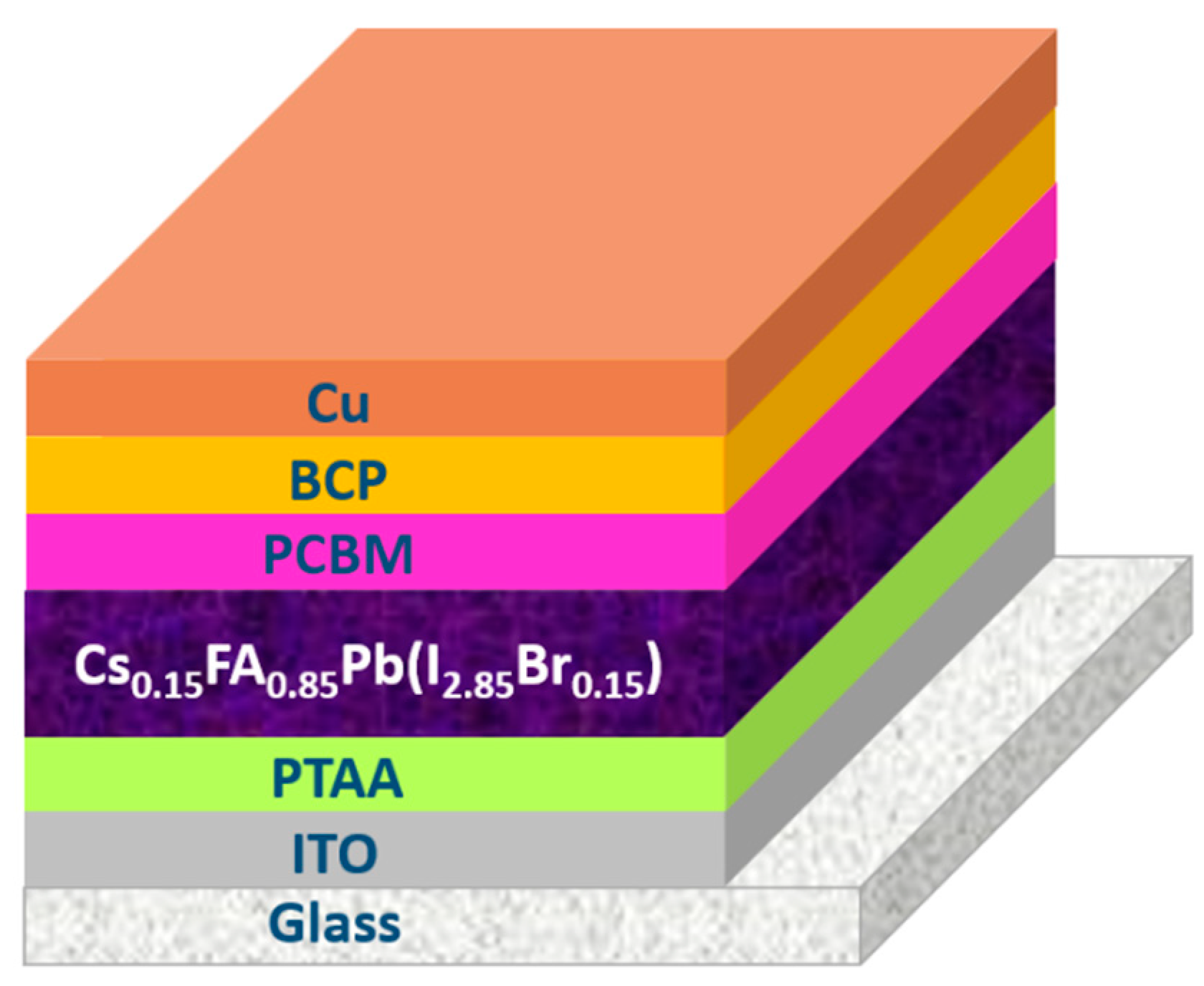
2. Materials and Methods

The device structure is shown in Figure 1, and the fabrication process has been described in detail in a previous work [27]. We investigated three different active layer thicknesses: 350, 500 and 650 nm, three samples of each thickness, each one having four devices, that is, 12 nominally equal cells for each thickness.
Electrical measurements were carried out using an Autolab potentiostat/galvanostat model PGSTAT204 (Eco-Chemie), equipped with the FRA32M impedance module and the Metrohm Autolab optical bench. The instrument was controlled by the NOVA 2.1.4 software. J-V characteristics were performed under 1000 W·m−2 illumination (equivalent to 1-sun) with an AM1.5G spectrum using an LED-based Solar Simulator (model Newport Oriel Verasol-2 class AAA).
Reverse and forward J-V curves recorded using a scan rate of 33 mV/s showed no hysteresis behavior. For this reason, J-V curves have been registered in forward direction (from JSC to VOC) using this scan rate and the characteristic parameters have been determined.
In order to study device degradation, indoor cell lifetime testing was carried out according to the International Summit on OSC Stability (ISOS) standard L-1 protocol [28]. During these experiments, cells were constantly irradiated under 1-sun illumination with controlled temperature and humidity conditions, and J-V characteristics were recorded every minute.
During the degradation experiment, IS characterization was carried out under light conditions at different bias voltages. Impedance spectra are obtained by applying a small AC voltage superimposed to a DC voltage and measuring the resulting AC current response. Impedance is defined as the small AC voltage over the resulting AC current, resulting in a frequency-dependent complex value. Cole–Cole diagram is obtained by plotting imaginary vs. real part of the impedance, with the frequency of an implicit parameter. Frequency ranged between 1 MHz and 1 Hz, applying sinusoidal signals of 50 mV amplitude under open-circuit conditions. Experimental data were modeled using Scribner’s ZView software.
Once the samples were stabilized, J-V characterization in a broad range of DC light intensities was carried out using the solar simulator. To evaluate the dominant recombination processes in the device, the ideality factor (n) was extracted from these DC measurements and compared with that extracted from the AC measurements.

3. Results and Discussion

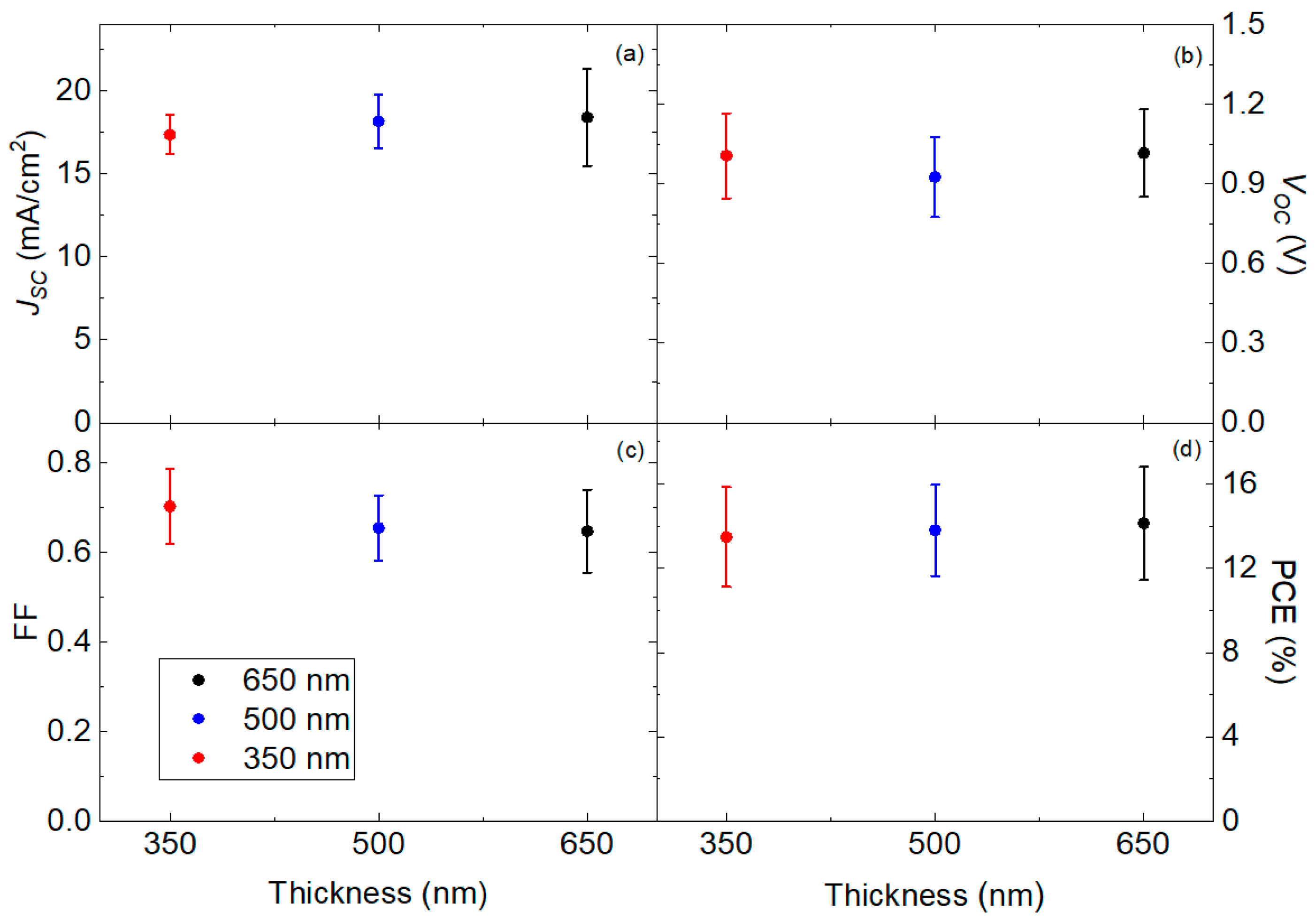
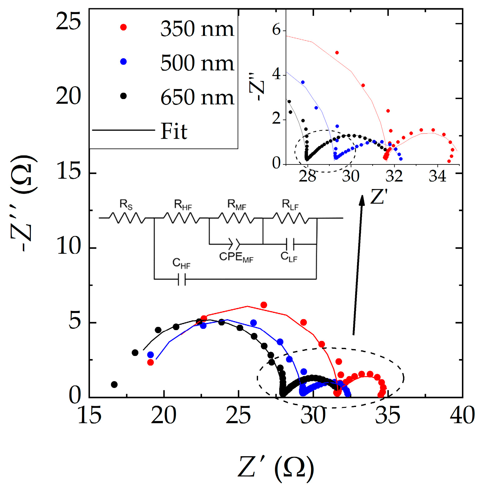
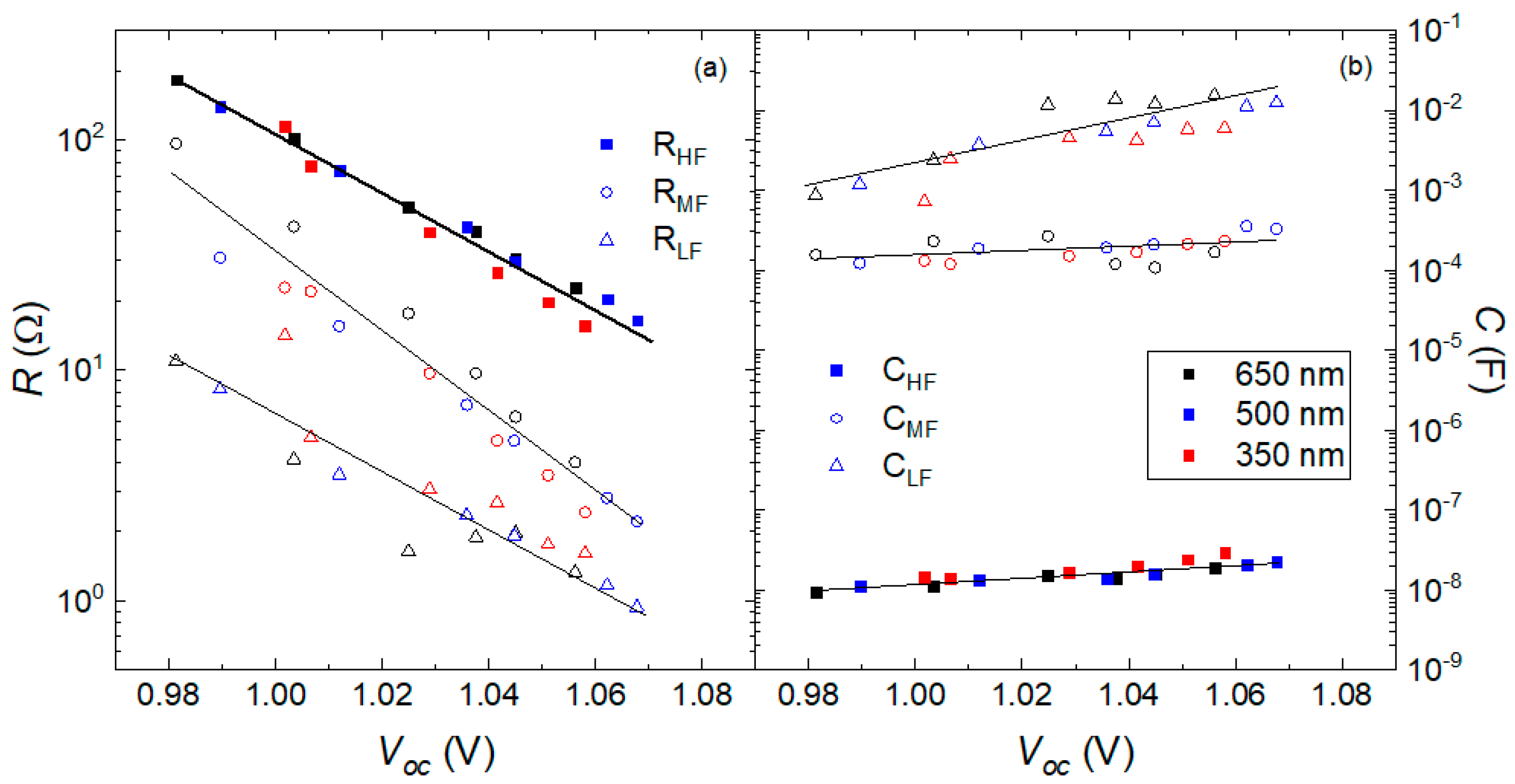
3.1. Pristine Characterization

Figure 2 shows the solar cell parameters, JSC, VOC, fill factor (FF) and PCE, for pristine devices for the three different active layer thicknesses. Champion cell efficiency was 17.05% for a 650 nm thick sample and no significant dependence of the efficiency on the active layer thickness was observed. The trade-off between higher carrier absorption (in thicker devices) and more efficient carrier extraction (in thinner devices) is responsible for the nearly constant efficiency with thickness measured in pristine devices.
In order to obtain a deeper insight into the dynamical physical mechanisms taking place in the device, samples were characterized using IS technique. Frequency is varied in order to observe dynamical mechanisms occurring from 1 µs, such as carrier transport, up to 1 s, such as ion diffusion. The different physical processes occurring in the device appear in the impedance spectra as distinctive features (arcs, loops, etc.) at different characteristic frequencies [29,30,31].
The impedance spectra of perovskite solar cells typically show two or three arcs [32,33,34]. The high frequency arc is usually related to charge recombination, but there is no consensus about the physical interpretation of the medium and low frequency features. They have been previously attributed to device degradation, a “giant dielectric” effect [35,36], electron accumulation at the contacts [37,38] and ionic diffusion [39]. Pockett et al. suggested that the medium and low frequency relaxation processes are due to a coupled electronic–ionic impedance, e.g., where the distribution of ions in the perovskite is able to modify the rate of carrier recombination [40]. Figure 3 shows the Nyquist plots of pristine devices for the three active layer thicknesses at VOC under 1-sun. At first sight, the spectra seem to have two distinctive semicircles. However, if the low frequency region is zoomed in (inset of Figure 3), a third medium frequency arc can be observed (dotted line in the inset). As we will present later, this third feature enhances with degradation.
Equivalent circuit modeling is used to quantify the resistive and capacitive contributions to the impedance spectrum over the measured frequency range. In this case, electrical parameters were obtained from the fit using the circuit shown in Figure 3. This is the hybrid Voight–Matryoshka configuration [34]. The circuit is a combination of the external series resistance (RS), three resistive elements (RHF, RMF and RLF), two ideal capacitors (CHF and CLF) and one non-ideal capacitive element named constant-phase element (CPEMF). The impedance of a CPE is given by Z CPE = 1 / [ Q ( j ω ) α ] [41], where Q is a parameter with units F·(Hz)(1−α). CHF represents the geometrical capacitance, which dominates the capacitive response in the high frequency region of the diagram, and it is associated with the dielectric constant of the perovskite layer (ε). CMF and CLF are medium and low frequency capacitances, respectively, where CMF is an effective capacitance defined as C MF = ( Q · R MF ) 1 / α · R M F 1 . The low frequency capacitance, CLF, has been related to ion diffusion and, eventually, ionic accumulation at the interfaces of the perovskite and the selective contacts [38]. On the other hand, the origin of CMF is still under debate. Moreover, the resistance RS models ohmic contribution of the contacts and wires, RHF is associated to carrier recombination, and RMF and RLF have been previously associated with several processes such as surface resistance, carrier accumulation resistance at the interfaces and slow processes, such as ion diffusion and trap-mediated charge recombination in the bulk [37,42,43]. In order to elucidate the physical processes governing the carrier dynamics at every time scale, a thorough analysis of the circuital parameters and their dependence on the VOC was performed.
Impedance spectra for different illumination intensities ranging from 0.1 up to 1-sun were measured at VOC and fitted with the electrical equivalent circuit described above for the three thicknesses. Figure 4 shows the electrical parameters (resistances and capacitances), obtained from the fits versus VOC.
As expected, we did not observe a significant dependence of the parameters on the active layer thickness, since ideally R and C depend on the active layer area but not on its thickness. However, in order to distinguish any slight dependence on active layer thickness, experimental data were analyzed separately when obtaining the ideality factor of the cells. The three resistive elements (RHF, RMF and RLF) show a negative exponential dependence on the VOC (Figure 4a). From the dependence of RHF, traditionally associated with the recombination resistance, the ideality factor of the diodes was extracted. Values are shown in Table 1 as well as the ideality factor obtained from DC measurements (VOC vs. illumination intensity [39]). RLF shows a similar trend, and, according to Zarazua et al. [43], both resistances are linked to the same physical process, thus, we also extracted the ideality factor from its dependence on VOC. Values are shown in Table 1. It can be observed that the ideality factors obtained from RLF, RHF and DC measurements are similar, confirming the hypothesis that those parameters model the same dynamical process. These ideality factors range between 1.2 and 1.5, suggesting that Shockley Read Hall (SRH) recombination is the dominant recombination mechanism in the devices [44].
High and medium frequency capacitances remain almost constant with the irradiation level. Traditionally CHF is related to the geometrical capacitance and its slight increase with VOC could be due to thermal effects after being exposed to prolonged illumination [45]. On the other hand, low frequency capacitance, CLF, also exhibits an exponential dependence with VOC (Figure 4b). From this dependence, we also calculated the ideality factor (see Table 1). These values are similar to those obtained from the high and low frequency resistances. According to Zarazua et al. [43], this opposite behavior of the low frequency capacitance, CLF, and the resistances RLF and RHF, suggests that these parameters are linked to the same physical process (carrier recombination). The physical meaning of the two resistances associated with CLF remains unclear. The same authors suggest that these resistances might model different capturing processes for electrons and holes, respectively, to a surface recombination center, where the recombination event would finally take place.
Regarding CMF, since it does not depend on the irradiation level, it could be related to an undesirable low-conductivity intermediate layer. This behavior has already been observed in organic solar cells [46].

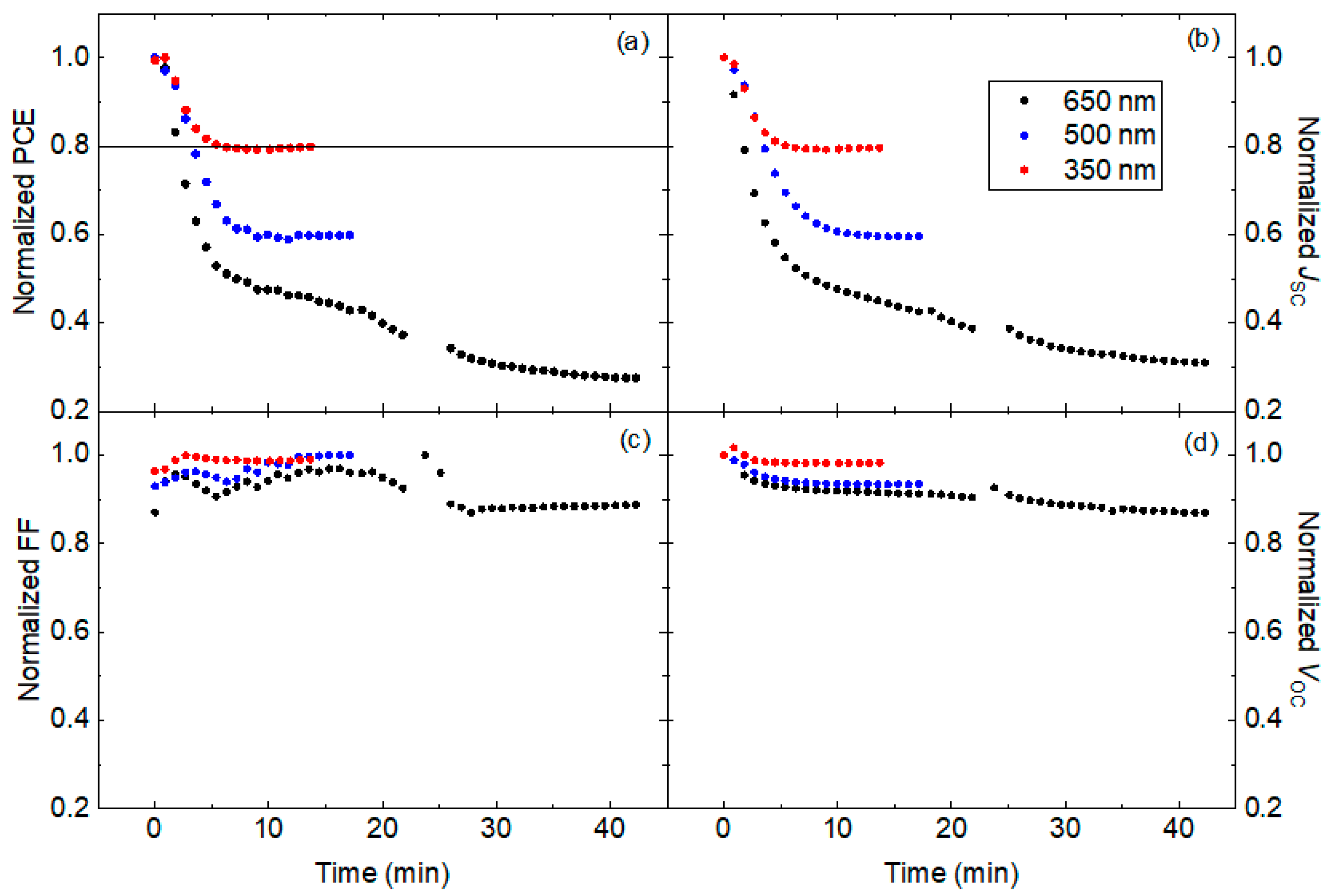
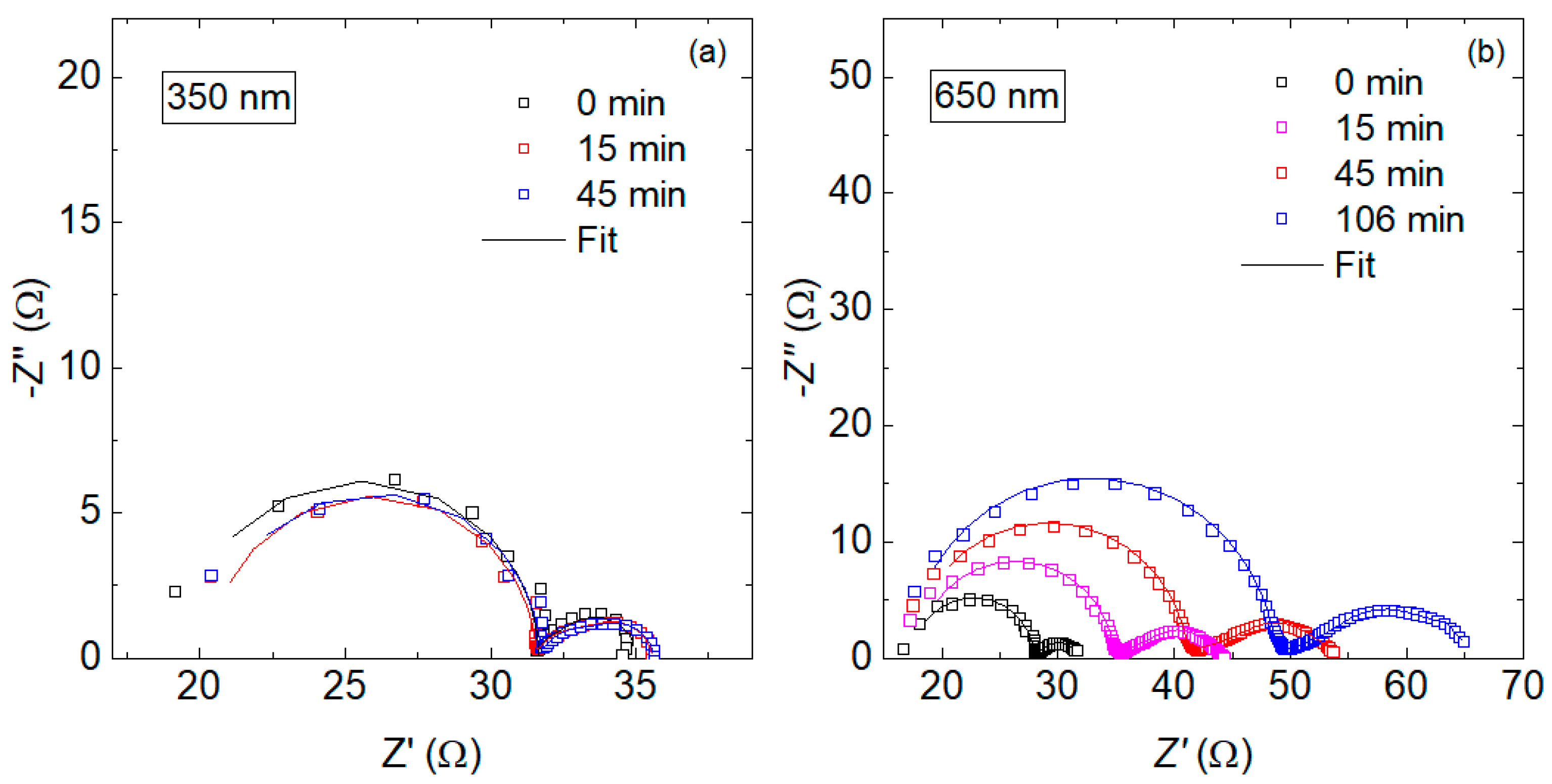
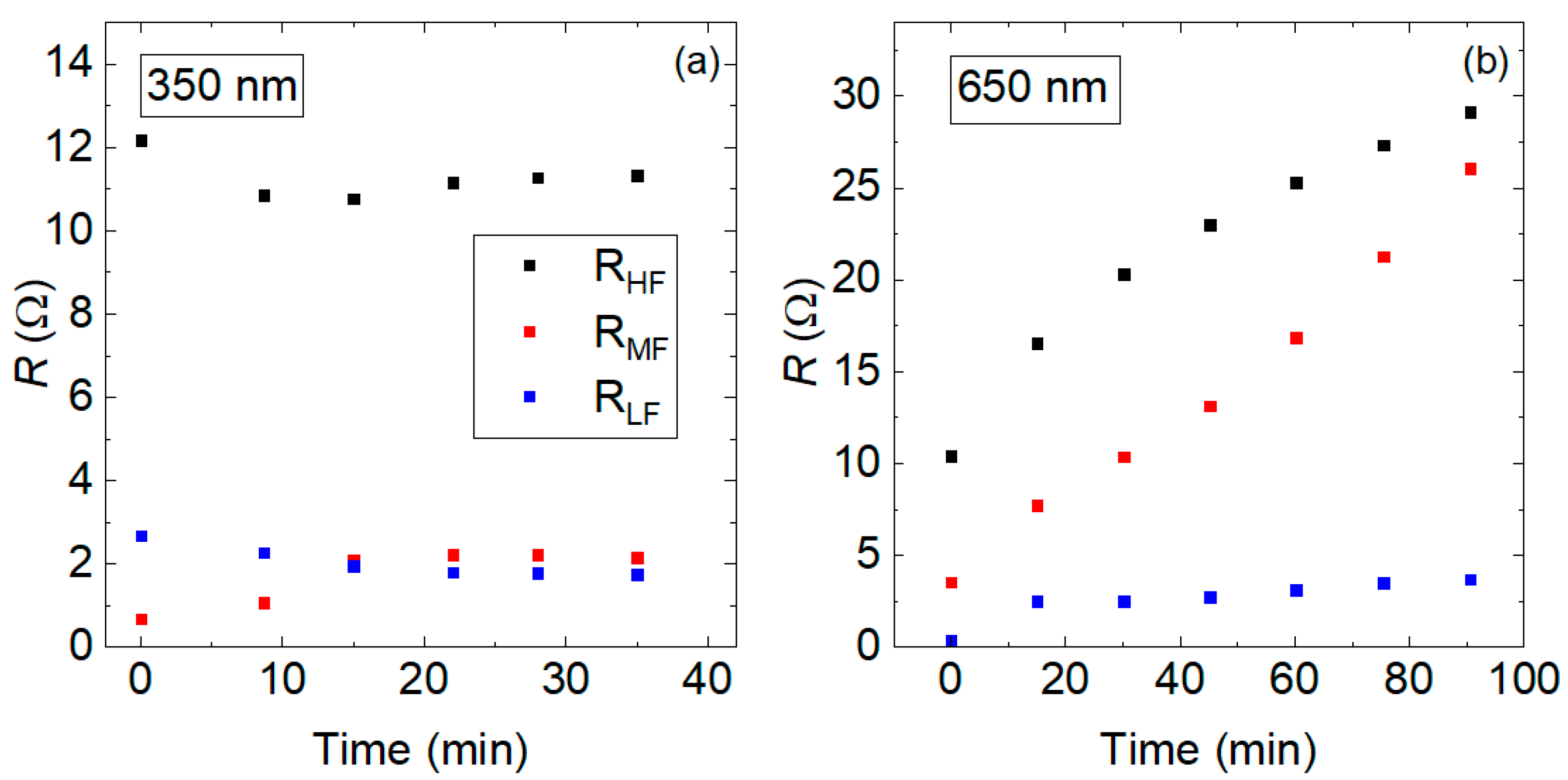
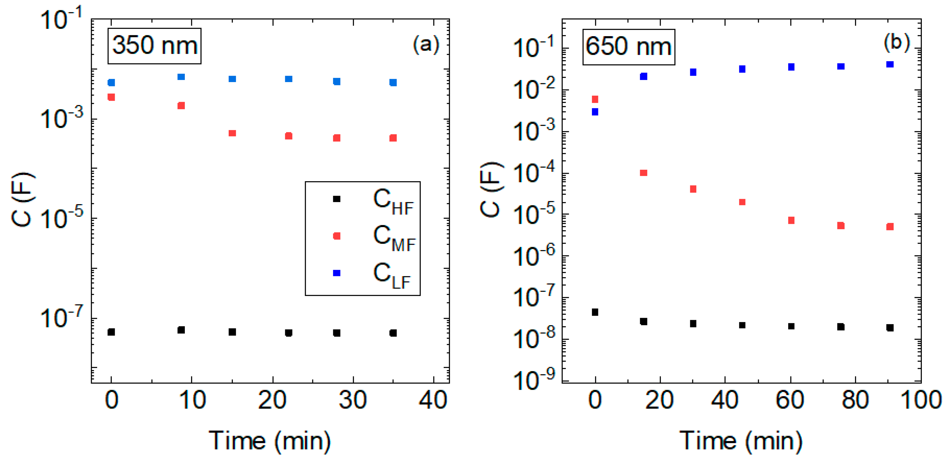
3.2. Degradation Characterization

In order to characterize cell degradation, we monitored the J-V curves of cells under one sun illumination until the efficiency stabilized.
Figure 5 shows the time evolution of the normalized parameters of one typical cell for the three different thicknesses. We observe a fast and abrupt decay of the cell efficiency during the first minutes of degradation. This dramatic drop in the efficiency is commonly found in organic [47] and perovskite [48] solar cells, and it is known as the “burn-in” effect. The causes of this burn-in degradation have been previously attributed to a worsening of the current extraction, energy transfer, or enhancing of non-radiative recombination, and/or the formation of trap states in the bandgap [49].
As we can observe in Figure 5, the time evolution of the efficiency for the three active layer thicknesses shows similar trends but different degradation parameters, T80 and stabilization times. Thin samples stabilize faster losing only 20% of their initial value. For medium samples, the stabilization takes almost the same time, around 5 min, but the decrease in the efficiency is almost 40% of the initial value. Finally, the worst scenario is found in the thickest samples, where the efficiency does not stabilize within the first 40 min of operation, reaching values lower than 30% of the initial efficiency.
On the other hand, the efficiency decay is dominated in all samples by a dramatic drop in JSC, which decreases by a similar percentage, while VOC and FF barely change (Figure 5).
Impedance measurements were carried out in similar samples during the degradation experiments, starting after the burn-in process. Results of the IS characterization can be found in Figure 6, where Nyquist plots for the 350 nm (a) and 650 nm (b) samples are represented at different degradation stages. After 45 min of degradation, the thinner sample does not show any significant change in the Cole–Cole diagram. However, for the thickest sample, a significant increase in both the high frequency and the medium–low frequency arcs, is observed.
Cole–Cole diagrams at different degradation stages for the 350 nm and 650 nm were fitted with the equivalent circuit described above.
Figure 7 and Figure 8 present the evolution of the circuital capacitances and resistances with the irradiation time for the thinnest (a) and thickest (b) sample, respectively. In the case of 350 nm, low and high frequency parameters do not vary significantly. Regarding medium frequency parameters, RMF increases while CMF decreases, which yields an increment in the medium frequency impedance. As has been previously mentioned, the authors believe that this feature is associated with the impedance of a low-conductivity intermediate layer. The reduction in CMF is clearly more pronounced in the 65 nm device, falling from 5.8 × 10⁻³ F down to 5 × 10⁻⁶ F. This huge drop, together with the increase in RMF in an order of magnitude, from 3 up to 27 Ω, yields to a dramatic increase in medium frequency impedance. This remarkable rise supports our hypothesis of the appearance of a low-conductivity intermediate layer for the thickest devices. We believe that this intermediate layer is directly related to an inefficient carrier extraction caused by the accumulation of mobile ions at one or both active layer interfaces, as will be discussed and supported by numerical simulations in the next section.
On the other hand, the RHF of the 650 nm sample increases with time, which is in good agreement with the reduction in the photogenerated current in this type of device.
Finally, a strong and fast increase in the CLF in the first 20 min of operation, from 3 × 10⁻³ F up to 4 × 10⁻² F, is observed. This capacitance, usually attributed to mobile ions, suggests an increase in the ionic mobile species in the device, which is in good agreement with the hypothesis of ion accumulation in the device.

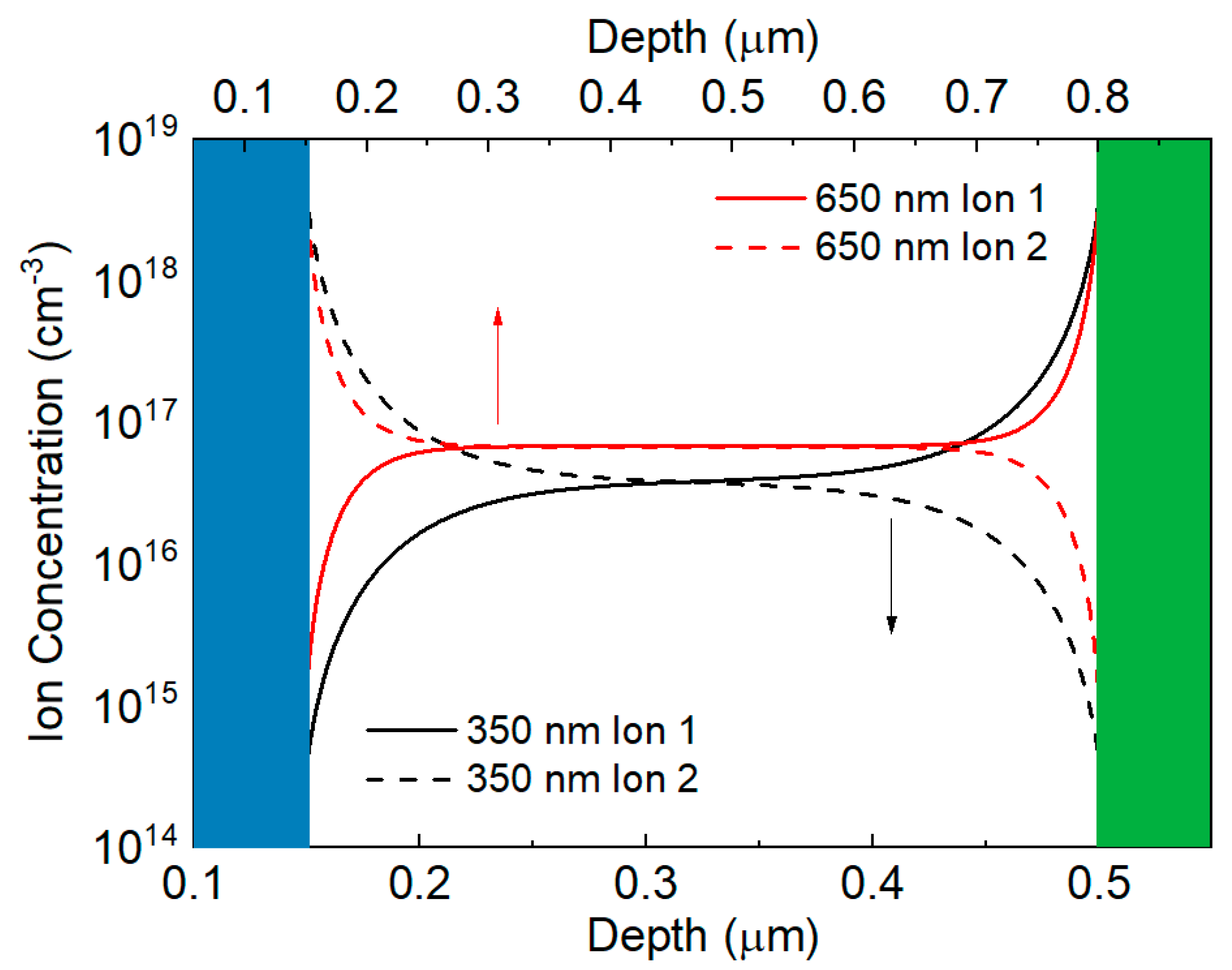
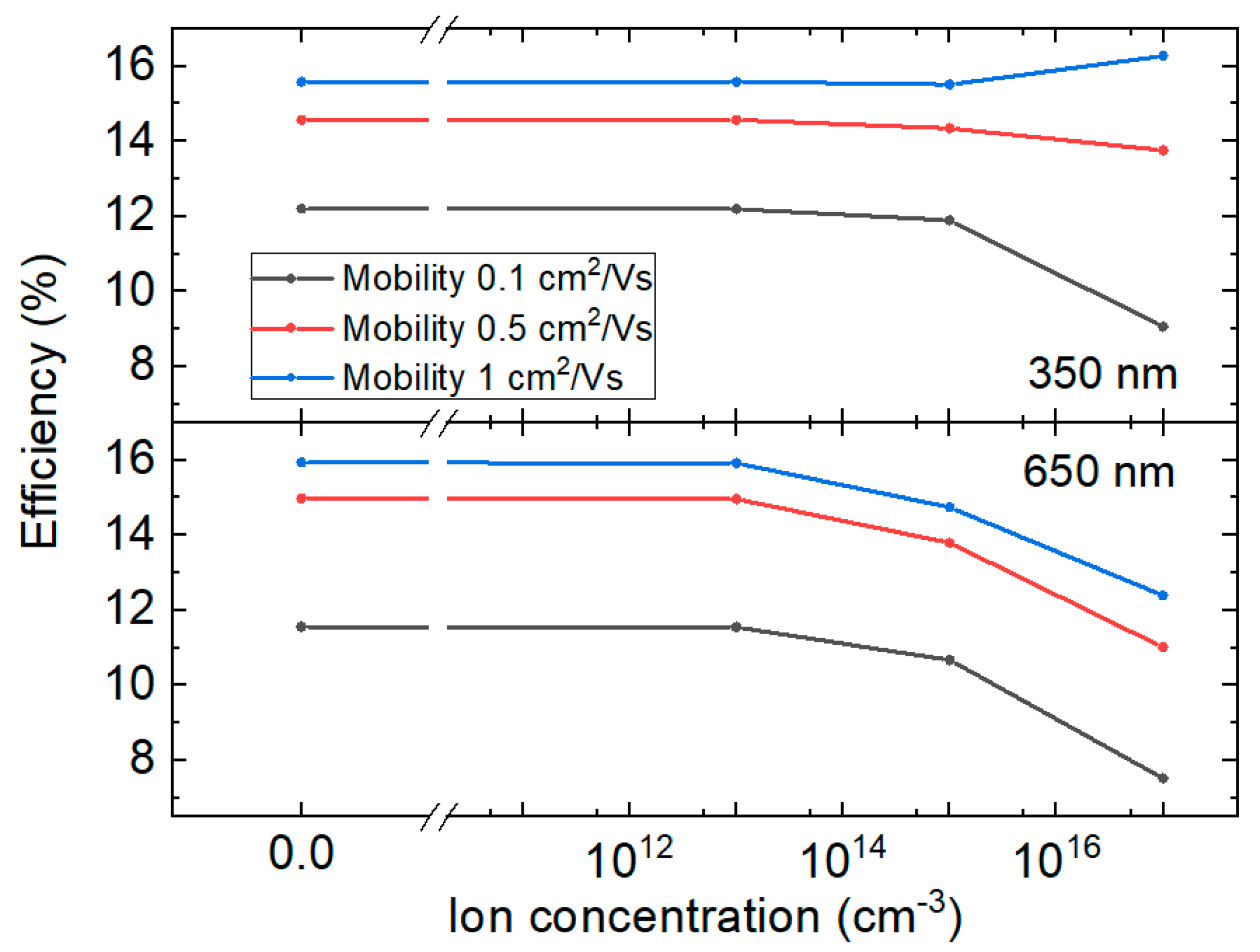
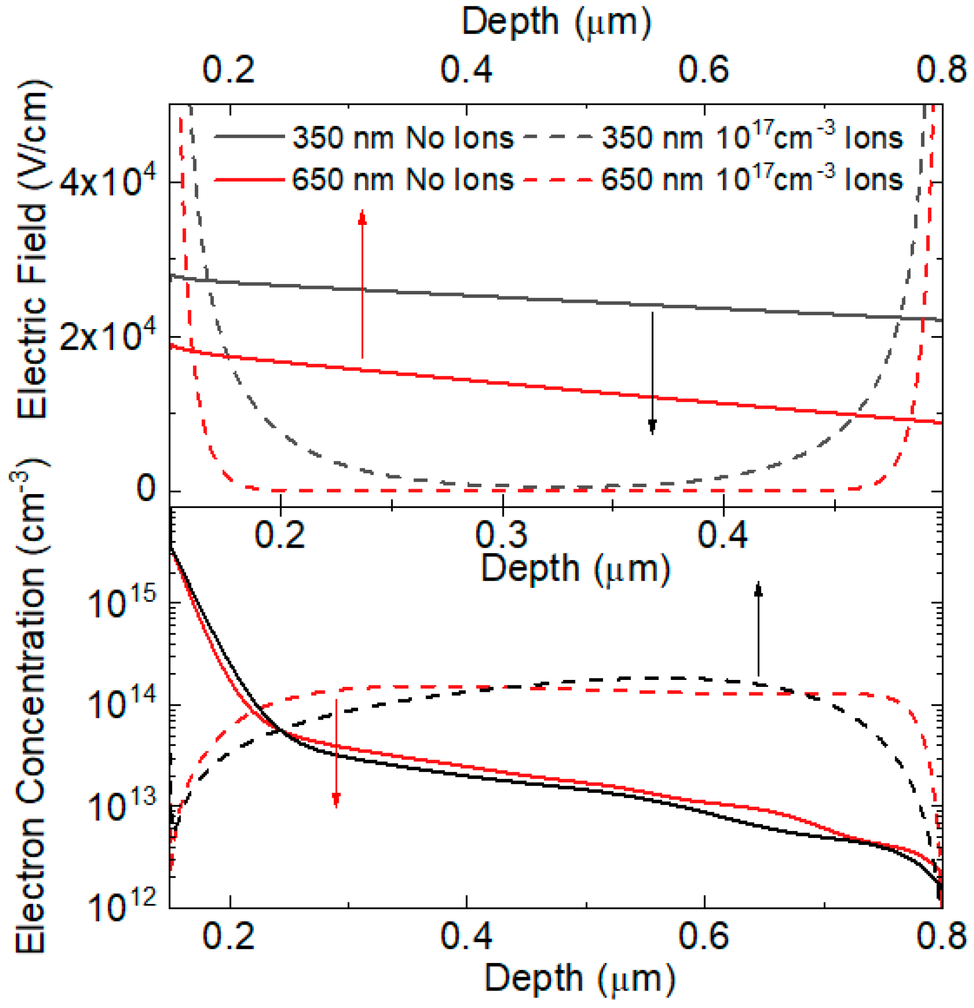
3.3. Numerical Simulations

In order to support our previous hypothesis, we performed 2D numerical simulations using SILVACO ATLAS TCAD software. In addition to the typical electronic behavior, we modeled the transport of two ionic mobile species with both positive (cations) and negative (anions) charges, both present in the active layer at an initial constant concentration. According to Bertoluzzi et al. [50], the mobile vacancy density for various halide perovskite is as high as 1017 cm−3, i.e., higher than the 1015 cm−3 residual P-type doping assumed for the perovskite active layer. In our case, the simulated device structure consists of an MAPI perovskite active layer with variable thickness, capped with a standard hole transport layer (HTL) and the electron transport layer (ETL). Anions and cations can move just within the active layer. All of our numerical simulations with Silvaco ATLAS TCAD start computing the carrier concentrations in the complete 2D structure at an external applied bias of 0 V and without illumination. After that, external bias and/or illumination is applied in several small steps to assure convergence and numerical accuracy, up to their final values.
Simulation results show that the constant initial mobile ion distribution rearranges depending on the absence or presence of external bias voltage and illumination, as was expected. In particular, when the device is illuminated under 1-sun AM1.5G and no external voltage is applied (short circuit conditions), the inner built-in electric field forces the positive (negative) mobile ions to travel to the cathode (anode), creating an inhomogeneous distribution displayed in Figure 9. It is shown that the resulting ion distribution along the perovskite film is mainly homogeneous in the central part of the active layer, except for the interfaces with the ETL and HTL layers, where mobile ions accumulate. This ion rearrangement creates charged interfacial layers whose thickness and peak charge strongly depend on the perovskite thickness, in accordance with the results from the IS analysis in the previous section. On the other hand, when a positive voltage close to VOC is applied (+1 V), the direction of the internal electric field inside the device changes sign, and mobile ions are forced to redistribute traveling to the opposite electrode.
To obtain further insight into the impact of the mobile ion redistribution in the device performance, Figure 10 shows the simulated device conversion efficiency as a function of the ion concentration (equal for anions and cations) for three different carrier mobilities (electron and hole) in the active layer. It is demonstrated that for 650 nm films, efficiency always drops as long as the ion concentration exceeds 1013 cm−3, regardless of the carrier mobility. In all cases, when the ion concentration increases, the electric field inside the perovskite decreases. Thus, the photogenerated charge extraction is not drift-assisted. In addition, Figure 10 shows that for the 350 nm active layer, the efficiency reduces only when carrier mobility is low and ion concentration is higher than 1015 cm−3, in accordance with the results from Bertoluzzi et al. [50]. This is because perovskite films with higher electron and hole mobilities have enhanced diffusion currents, so carriers do not rely on the internal electric field to move along the layer. Moreover, thinner films inherently present higher electric fields due to steeper gradients in their energy band structure, as is shown in Figure 11.
Figure 11 also shows that, at short circuit conditions, the internal electric field inside the device dramatically changes when including mobile ions in the simulation. For both device thicknesses, 350 nm and 650 nm, the electric field decreases becoming almost negligible in the central part of the active layer, and this is more pronounced for the thickest device. In the absence of or at low ion concentrations, the electric field is lower in the thicker layers, but it is still high enough to obtain an efficient current extraction, in accordance with the measured high PCE for pristine devices.
On the other hand, the carrier concentration in pristine devices presents a similar profile (Figure 11), with carriers being accumulated at the HTL interface and extracted at the ETL contact, as expected. However, when ions are included in the simulation, carriers remain accumulated in the middle of the active layer, and extraction is less efficient. This effect is more pronounced in thicker devices, where carriers accumulate almost along all of the active layer due to the lower electric field.

4. Conclusions

In this work, we have measured J-V and IS in perovskite solar cells based on CsFAPbIBr with different active layer thicknesses, from 350 nm to 650 nm. The cell performance in a pristine state is not affected significantly by changes in the active layer thickness. Similar ideality factors, n =1.2–1.5, have been obtained from the dependence of the RLF, CLF and RHF on VOC, indicating that SRH is the main recombination mechanism. Interestingly, the degradation pattern varies significantly depending on the perovskite thickness. The thickest samples, 650 nm, show a more pronounced burn-in process and no stabilization of the cell efficiency when compared to 350 and 500 nm samples. Moreover, IS measurements at different degradation stages show three distinctive features that have been fitted with a three RC/CPE elements equivalent circuit. CLF rises with degradation time in the 650 nm cell, indicating an increase in the ionic mobile species. Moreover, the medium frequency impedance increases dramatically as a result of a significant decay of CMF and RMF increasing an order of magnitude. This medium frequency behavior is attributed to the appearance of a low-conductivity intermediate layer for the thickest devices. Finally, numerical simulations reveal that this higher ion population partially screens the electric field in the perovskite, which is ultimately responsible for the reduction in the carrier extraction and, therefore, in the cell efficiency. Therefore, we can conclude that for this configuration, thickness is not a determinant for pristine device performance but results in a key parameter when searching for better long-term stability.

Author Contributions

All authors contributed to the manuscript and were involved in the discussion of results. Device manufacture, Y.G. and M.N.; characterization and circuital modeling, M.C.L.-G., L.M.-D., J.C.P.-M., G.d.P. and E.H.-B.; data processing, M.C.L.-G., L.M.-D. and J.C.P.-M.; physical simulations, D.M.-M. and G.d.P.; writing-review and editing, B.A., B.R. and M.C.L.-G.; funding acquisition, B.A., B.R. and Y.G. All authors have read and agreed to the published version of the manuscript.

Funding

This research was funded by Comunidad de Madrid under the SINFOTON2-CM Research Program (S2018/NMT-4326-SINFOTON2-CM), and by Universidad Rey Juan Carlos with research projects “Materiales nanoensamblados para sensado y manipulación de luz en amplio rango spectral”, reference M2417, and by the Community of Madrid in the framework of the Multiannual Agreement with the Rey Juan Carlos University in line of action 1, “Encouragement of Young Phd students investigation” Project Ref. M2180, “SolGenALEE”, and “Grupo DELFO de alto rendimiento”, reference M2363, under research program “Programa de fomento y desarrollo de la investigación”. Y.G. acknowledges the Ministry of Science and Technology of Taiwan (MOST) for the financial support provided by grant with project number 110-2222-E-002-001-MY3, and by National Taiwan University with grant number 110L104042.

Conflicts of Interest

The authors declare no conflict of interest.

References

  1. Frost, J.M.; Butler, K.T.; Brivio, F.; Hendon, C.H.; van Schilfgaarde, M.; Walsh, A. Atomistic Origins of High-Performance in Hybrid Halide Perovskite Solar Cells. Nano Lett. 2014, 14, 2584–2590. [Google Scholar] [CrossRef] [PubMed] [Green Version]
  2. NREL Efficiency Chart. This Plot Is Courtesy of the National Renewable Energy Laboratory, Golden, CO. Available online: https://www.nrel.gov/pv/assets/pdfs/best-research-cell-efficiencies-rev211117.pdf (accessed on 24 November 2021).
  3. Di Giacomo, F.; Fakharuddin, A.; Jose, R.; Brown, T.M. Progress, Challenges and Perspectives in Flexible Perovskite Solar Cells. Energy Environ. Sci. 2016, 9, 3007–3035. [Google Scholar] [CrossRef] [Green Version]
  4. Snaith, H.J.; Abate, A.; Ball, J.M.; Eperon, G.E.; Leijtens, T.; Noel, N.K.; Stranks, S.D.; Wang, J.T.-W.; Wojciechowski, K.; Zhang, W. Anomalous Hysteresis in Perovskite Solar Cells. J. Phys. Chem. Lett. 2014, 5, 1511–1515. [Google Scholar] [CrossRef] [PubMed]
  5. Elumalai, N.K.; Uddin, A. Hysteresis in Organic-Inorganic Hybrid Perovskite Solar Cells. Sol. Energy Mater. Sol. Cells 2016, 157, 476–509. [Google Scholar] [CrossRef]
  6. Correa-Baena, J.-P.; Saliba, M.; Buonassisi, T.; Grätzel, M.; Abate, A.; Tress, W.; Hagfeldt, A. Promises and Challenges of Perovskite Solar Cells. Science 2017, 358, 739–744. [Google Scholar] [CrossRef] [Green Version]
  7. Wang, T.-L.; Yang, C.-H.; Chuang, Y.-Y. A Comparative Study of the Effect of Fluorine Substitution on the Photovoltaic Performance of Benzothiadiazole-Based Copolymers. RSC Adv. 2016, 6, 47676–47686. [Google Scholar] [CrossRef]
  8. Xu, K.J.; Wang, R.T.; Xu, A.F.; Chen, J.Y.; Xu, G. Hysteresis and Instability Predicted in Moisture Degradation of Perovskite Solar Cells. ACS Appl. Mater. Interfaces 2020, 12, 48882–48889. [Google Scholar] [CrossRef] [PubMed]
  9. Aristidou, N.; Eames, C.; Sanchez-Molina, I.; Bu, X.; Kosco, J.; Islam, M.S.; Haque, S.A. Fast Oxygen Diffusion and Iodide Defects Mediate Oxygen-Induced Degradation of Perovskite Solar Cells. Nat. Commun. 2017, 8, 15218. [Google Scholar] [CrossRef] [PubMed]
  10. Bryant, D.; Aristidou, N.; Pont, S.; Sanchez-Molina, I.; Chotchunangatchaval, T.; Wheeler, S.; Durrant, J.R.; Haque, S.A. Light and Oxygen Induced Degradation Limits the Operational Stability of Methylammonium Lead Triiodide Perovskite Solar Cells. Energy Environ. Sci. 2016, 9, 1655–1660. [Google Scholar] [CrossRef] [Green Version]
  11. Lee, S.-W.; Kim, S.; Bae, S.; Cho, K.; Chung, T.; Mundt, L.E.; Lee, S.; Park, S.; Park, H.; Schubert, M.C.; et al. UV Degradation and Recovery of Perovskite Solar Cells. Sci. Rep. 2016, 6, 38150. [Google Scholar] [CrossRef] [PubMed] [Green Version]
  12. Farooq, A.; Hossain, I.M.; Moghadamzadeh, S.; Schwenzer, J.A.; Abzieher, T.; Richards, B.S.; Klampaftis, E.; Paetzold, U.W. Spectral Dependence of Degradation under Ultraviolet Light in Perovskite Solar Cells. ACS Appl. Mater. Interfaces 2018, 10, 21985–21990. [Google Scholar] [CrossRef] [PubMed]
  13. Papež, N.; Gajdoš, A.; Dallaev, R.; Sobola, D.; Sedlák, P.; Motúz, R.; Nebojsa, A.; Grmela, L. Performance Analysis of GaAs Based Solar Cells under Gamma Irradiation. Appl. Surf. Sci. 2020, 510, 145329. [Google Scholar] [CrossRef]
  14. Misra, R.K.; Aharon, S.; Li, B.; Mogilyansky, D.; Visoly-Fisher, I.; Etgar, L.; Katz, E.A. Temperature- and Component-Dependent Degradation of Perovskite Photovoltaic Materials under Concentrated Sunlight. J. Phys. Chem. Lett. 2015, 6, 326–330. [Google Scholar] [CrossRef]
  15. Abdelmageed, G.; Mackeen, C.; Hellier, K.; Jewell, L.; Seymour, L.; Tingwald, M.; Bridges, F.; Zhang, J.Z.; Carter, S. Effect of Temperature on Light Induced Degradation in Methylammonium Lead Iodide Perovskite Thin Films and Solar Cells. Sol. Energy Mater. Sol. Cells 2018, 174, 566–571. [Google Scholar] [CrossRef]
  16. Back, H.; Kim, G.; Kim, J.; Kong, J.; Kim, T.K.; Kang, H.; Kim, H.; Lee, J.; Lee, S.; Lee, K. Achieving Long-Term Stable Perovskite Solar Cells via Ion Neutralization. Energy Environ. Sci. 2016, 9, 1258–1263. [Google Scholar] [CrossRef]
  17. Li, J.; Dong, Q.; Li, N.; Wang, L. Direct Evidence of Ion Diffusion for the Silver-Electrode-Induced Thermal Degradation of Inverted Perovskite Solar Cells. Adv. Energy Mater. 2017, 7, 1602922. [Google Scholar] [CrossRef]
  18. Saliba, M.; Matsui, T.; Seo, J.-Y.; Domanski, K.; Correa-Baena, J.-P.; Nazeeruddin, M.K.; Zakeeruddin, S.M.; Tress, W.; Abate, A.; Hagfeldt, A.; et al. Cesium-Containing Triple Cation Perovskite Solar Cells: Improved Stability, Reproducibility and High Efficiency. Energy Environ. Sci. 2016, 9, 1989–1997. [Google Scholar] [CrossRef] [PubMed] [Green Version]
  19. Mateen, M.; Arain, Z.; Liu, X.; Liu, C.; Yang, Y.; Ding, Y.; Ma, S.; Ren, Y.; Wu, Y.; Tao, Y.; et al. High-Performance Mixed-Cation Mixed-Halide Perovskite Solar Cells Enabled by a Facile Intermediate Engineering Technique. J. Power Sources 2020, 448, 227386. [Google Scholar] [CrossRef]
  20. Lee, J.-W.; Kim, D.-H.; Kim, H.-S.; Seo, S.-W.; Cho, S.M.; Park, N.-G. Formamidinium and Cesium Hybridization for Photo- and Moisture-Stable Perovskite Solar Cell. Adv. Energy Mater. 2015, 5, 1501310. [Google Scholar] [CrossRef]
  21. Chai, L.; Zhong, M.; Li, X.; Wu, N.; Zhou, J. The Effect of Bromine Doping on the Perovskite Solar Cells Modified by PVP/PEG Polymer Blends. Superlattices Microstruct. 2018, 120, 279–287. [Google Scholar] [CrossRef]
  22. Tu, Y.; Wu, J.; Lan, Z.; He, X.; Dong, J.; Jia, J.; Guo, P.; Lin, J.; Huang, M.; Huang, Y. Modulated CH3NH3PbI3−xBrx Film for Efficient Perovskite Solar Cells Exceeding 18%. Sci. Rep. 2017, 7, 44603. [Google Scholar] [CrossRef] [Green Version]
  23. Liu, D.; Gangishetty, M.K.; Kelly, T.L. Effect of CH3NH3PbI3 Thickness on Device Efficiency in Planar Heterojunction Perovskite Solar Cells. J. Mater. Chem. A 2014, 2, 19873–19881. [Google Scholar] [CrossRef] [Green Version]
  24. Zhang, B.; Zhang, M.-J.; Pang, S.-P.; Huang, C.-S.; Zhou, Z.-M.; Wang, D.; Wang, N.; Cui, G.-L. Carrier Transport in CH 3 NH 3 PbI 3 Films with Different Thickness for Perovskite Solar Cells. Adv. Mater. Interfaces 2016, 3, 1600327. [Google Scholar] [CrossRef]
  25. Chen, J.; Zuo, L.; Zhang, Y.; Lian, X.; Fu, W.; Yan, J.; Li, J.; Wu, G.; Li, C.-Z.; Chen, H. High-Performance Thickness Insensitive Perovskite Solar Cells with Enhanced Moisture Stability. Adv. Energy Mater. 2018, 8, 1800438. [Google Scholar] [CrossRef]
  26. Hernández-Balaguera, E.; Romero, B.; Arredondo, B.; del Pozo, G.; Najafi, M.; Galagan, Y. The Dominant Role of Memory-Based Capacitive Hysteretic Currents in Operation of Photovoltaic Perovskites. Nano Energy 2020, 78, 105398. [Google Scholar] [CrossRef]
  27. Arredondo, B.; Romero, B.; Sanchez Pena, J.M.; Fernandez-Pacheco, A.; Alonso, E.; Vergaz, R.; de Dios, C. Visible Light Communication System Using an Organic Bulk Heterojunction Photodetector. Sensors 2013, 13, 12266–12276. [Google Scholar] [CrossRef] [PubMed] [Green Version]
  28. Khenkin, M.V.; Katz, E.A.; Abate, A.; Bardizza, G.; Berry, J.J.; Brabec, C.; Brunetti, F.; Bulović, V.; Burlingame, Q.; Di Carlo, A.; et al. Consensus Statement for Stability Assessment and Reporting for Perovskite Photovoltaics Based on ISOS Procedures. Nat. Energy 2020, 5, 35–49. [Google Scholar] [CrossRef]
  29. von Hauff, E. Impedance Spectroscopy for Emerging Photovoltaics. J. Phys. Chem. C 2019, 123, 11329–11346. [Google Scholar] [CrossRef] [Green Version]
  30. Dualeh, A.; Moehl, T.; Tétreault, N.; Teuscher, J.; Gao, P.; Nazeeruddin, M.K.; Grätzel, M. Impedance Spectroscopic Analysis of Lead Iodide Perovskite-Sensitized Solid-State Solar Cells. ACS Nano 2014, 8, 362–373. [Google Scholar] [CrossRef]
  31. Pascoe, A.R.; Duffy, N.W.; Scully, A.D.; Huang, F.; Cheng, Y.-B. Insights into Planar CH3NH3PbI3 Perovskite Solar Cells Using Impedance Spectroscopy. J. Phys. Chem. C 2015, 119, 4444–4453. [Google Scholar] [CrossRef]
  32. Bou, A.; Pockett, A.; Raptis, D.; Watson, T.; Carnie, M.J.; Bisquert, J. Beyond Impedance Spectroscopy of Perovskite Solar Cells: Insights from the Spectral Correlation of the Electrooptical Frequency Techniques. J. Phys. Chem. Lett. 2020, 11, 8654–8659. [Google Scholar] [CrossRef] [PubMed]
  33. Contreras, L.; Ramos-Terrón, S.; Riquelme, A.; Boix, P.P.; Idígoras, J.A.; Seró, I.M.; Anta, J.A. Impedance Analysis of Perovskite Solar Cells: A Case Study. J. Mater. Chem. A 2019, 7, 12191–12200. [Google Scholar] [CrossRef]
  34. Todinova, A.; Contreras-Bernal, L.; Salado, M.; Ahmad, S.; Morillo, N.; Idígoras, J.; Anta, J.A. Towards a Universal Approach for the Analysis of Impedance Spectra of Perovskite Solar Cells: Equivalent Circuits and Empirical Analysis. ChemElectroChem 2017, 4, 2891–2901. [Google Scholar] [CrossRef]
  35. Juarez-Perez, E.J.; Sanchez, R.S.; Badia, L.; Garcia-Belmonte, G.; Kang, Y.S.; Mora-Sero, I.; Bisquert, J. Photoinduced Giant Dielectric Constant in Lead Halide Perovskite Solar Cells. J. Phys. Chem. Lett. 2014, 5, 2390–2394. [Google Scholar] [CrossRef] [PubMed]
  36. Almora, O.; Zarazua, I.; Mas-Marza, E.; Mora-Sero, I.; Bisquert, J.; Garcia-Belmonte, G. Capacitive Dark Currents, Hysteresis, and Electrode Polarization in Lead Halide Perovskite Solar Cells. J. Phys. Chem. Lett. 2015, 6, 1645–1652. [Google Scholar] [CrossRef] [PubMed]
  37. Guerrero, A.; Garcia-Belmonte, G.; Mora-Sero, I.; Bisquert, J.; Kang, Y.S.; Jacobsson, T.J.; Correa-Baena, J.-P.; Hagfeldt, A. Properties of Contact and Bulk Impedances in Hybrid Lead Halide Perovskite Solar Cells Including Inductive Loop Elements. J. Phys. Chem. C 2016, 120, 8023–8032. [Google Scholar] [CrossRef] [Green Version]
  38. Zarazua, I.; Bisquert, J.; Garcia-Belmonte, G. Light-Induced Space-Charge Accumulation Zone as Photovoltaic Mechanism in Perovskite Solar Cells. J. Phys. Chem. Lett. 2016, 7, 525–528. [Google Scholar] [CrossRef] [PubMed] [Green Version]
  39. Bag, M.; Renna, L.A.; Adhikari, R.Y.; Karak, S.; Liu, F.; Lahti, P.M.; Russell, T.P.; Tuominen, M.T.; Venkataraman, D. Kinetics of Ion Transport in Perovskite Active Layers and Its Implications for Active Layer Stability. J. Am. Chem. Soc. 2015, 137, 13130–13137. [Google Scholar] [CrossRef]
  40. Pockett, A.; Eperon, G.E.; Sakai, N.; Snaith, H.J.; Peter, L.M.; Cameron, P.J. Microseconds, Milliseconds and Seconds: Deconvoluting the Dynamic Behaviour of Planar Perovskite Solar Cells. Phys. Chem. Chem. Phys. 2017, 19, 5959–5970. [Google Scholar] [CrossRef] [Green Version]
  41. Hernández-Balaguera, E.; Arredondo, B.; del Pozo, G.; Romero, B. Exploring the Impact of Fractional-Order Capacitive Behavior on the Hysteresis Effects of Perovskite Solar Cells: A Theoretical Perspective. Commun. Nonlinear Sci. Numer. Simul. 2020, 90, 105371. [Google Scholar] [CrossRef]
  42. Hailegnaw, B.; Sariciftci, N.S.; Scharber, M.C. Impedance Spectroscopy of Perovskite Solar Cells: Studying the Dynamics of Charge Carriers Before and After Continuous Operation. Phys. Status Solidi A 2020, 217, 2000291. [Google Scholar] [CrossRef]
  43. Zarazua, I.; Han, G.; Boix, P.P.; Mhaisalkar, S.; Fabregat-Santiago, F.; Mora-Seró, I.; Bisquert, J.; Garcia-Belmonte, G. Surface Recombination and Collection Efficiency in Perovskite Solar Cells from Impedance Analysis. J. Phys. Chem. Lett. 2016, 7, 5105–5113. [Google Scholar] [CrossRef] [PubMed] [Green Version]
  44. Tress, W.; Yavari, M.; Domanski, K.; Yadav, P.; Niesen, B.; Baena, J.P.C.; Hagfeldt, A.; Graetzel, M. Interpretation and Evolution of Open-Circuit Voltage, Recombination, Ideality Factor and Subgap Defect States during Reversible Light-Soaking and Irreversible Degradation of Perovskite Solar Cells. Energy Environ. Sci. 2018, 11, 151–165. [Google Scholar] [CrossRef]
  45. Almora, O.; Aranda, C.; Garcia-Belmonte, G. Do Capacitance Measurements Reveal Light-Induced Bulk Dielectric Changes in Photovoltaic Perovskites? J. Phys. Chem. C 2018, 122, 13450–13454. [Google Scholar] [CrossRef]
  46. Arredondo, B.; Romero, B.; Beliatis, M.J.; del Pozo, G.; Martín-Martín, D.; Blakesley, J.C.; Dibb, G.; Krebs, F.C.; Gevorgyan, S.A.; Castro, F.A. Analysing Impact of Oxygen and Water Exposure on Roll-Coated Organic Solar Cell Performance Using Impedance Spectroscopy. Sol. Energy Mater. Sol. Cells 2018, 176, 397–404. [Google Scholar] [CrossRef]
  47. Kong, J.; Song, S.; Yoo, M.; Lee, G.Y.; Kwon, O.; Park, J.K.; Back, H.; Kim, G.; Lee, S.H.; Suh, H.; et al. Long-Term Stable Polymer Solar Cells with Significantly Reduced Burn-in Loss. Nat. Commun. 2014, 5, 5688. [Google Scholar] [CrossRef]
  48. Hang, P.; Xie, J.; Kan, C.; Li, B.; Zhang, Y.; Gao, P.; Yang, D.; Yu, X. Stabilizing Fullerene for Burn-in-Free and Stable Perovskite Solar Cells under Ultraviolet Preconditioning and Light Soaking. Adv. Mater. 2021, 33, 2006910. [Google Scholar] [CrossRef]
  49. Peters, C.H.; Sachs-Quintana, I.T.; Mateker, W.R.; Heumueller, T.; Rivnay, J.; Noriega, R.; Beiley, Z.M.; Hoke, E.T.; Salleo, A.; McGehee, M.D. The Mechanism of Burn-in Loss in a High Efficiency Polymer Solar Cell. Adv. Mater. 2012, 24, 663–668. [Google Scholar] [CrossRef]
  50. Bertoluzzi, L.; Boyd, C.C.; Rolston, N.; Xu, J.; Prasanna, R.; O’Regan, B.C.; McGehee, M.D. Mobile Ion Concentration Measurement and Open-Access Band Diagram Simulation Platform for Halide Perovskite Solar Cells. Joule 2020, 4, 109–127. [Google Scholar] [CrossRef]
Figure 1. Device layer structure layout. Note that scaling between layer thicknesses was not considered.
Applsci 11 11668 g001
Figure 2. Solar cell parameters, (a) JSC, (b) VOC, (c) FF and (d) PCE, for pristine devices with different active layer thickness: 350, 500 and 650 nm characterized under 1-sun AM1.5 illumination. The statistics were performed for 12 cells for each thickness.
Applsci 11 11668 g002
Figure 3. Nyquist plot of the pristine samples. Experimental measurements (symbols), circuital fit (solid line). Equivalent circuital model used to fit experimental IS.
Applsci 11 11668 g003
Figure 4. High, medium and low frequency (a) resistances and (b) capacitances vs. Voc for the 350, 500 and 650 nm active layer thickness. Solid lines have been plotted as a visual guide.
Applsci 11 11668 g004
Figure 5. Normalized characteristic parameters, (a) PCE, (b) JSC, (c) FF and (d) VOC, of the different samples as function of the illumination time. Missing points are discontinuities found when disconnecting the samples for IS characterization.
Applsci 11 11668 g005
Figure 6. Nyquist plots during degradation time of (a) 350 nm and (b) 650 nm samples.
Applsci 11 11668 g006
Figure 7. Evolution of resistances with irradiation time for (a) 350 nm and (b) 650 nm.
Applsci 11 11668 g007
Figure 8. Evolution of capacitances with irradiation time for (a) 350 nm and (b) 650 nm.
Applsci 11 11668 g008
Figure 9. Mobile ions (cations and anions) concentration profile along with the 350 nm and 650 nm active layers, under 1-sun illumination with the applied voltage set to 0 V (JSC conditions).
Applsci 11 11668 g009
Figure 10. Cell efficiency as a function of the ion concentration for three carrier mobilities (electron and hole), and for 350 nm and 650 nm devices.
Applsci 11 11668 g010
Figure 11. Electric field profile and electron concentration along the active layer at short circuit conditions. Active layer is 350 nm (black) and 650 nm (red) thick, and ion concentrations are set to 0 (line) and 1017 cm−3 (dashed).
Applsci 11 11668 g011
Table 1. Ideality factor extracted from DC and AC measurements.
Thickness (nm)n from VOCn from RHFn from RLFn from CLF
6501.21.41.51.2
5001.21.41.51.4
3501.31.21.21.3
Publisher’s Note: MDPI stays neutral with regard to jurisdictional claims in published maps and institutional affiliations.

