
Electrically Tunable Perfect Terahertz Absorber Using Embedded Combline Graphene Layer


Abstract
:1. Introduction
2. Theoretical Background
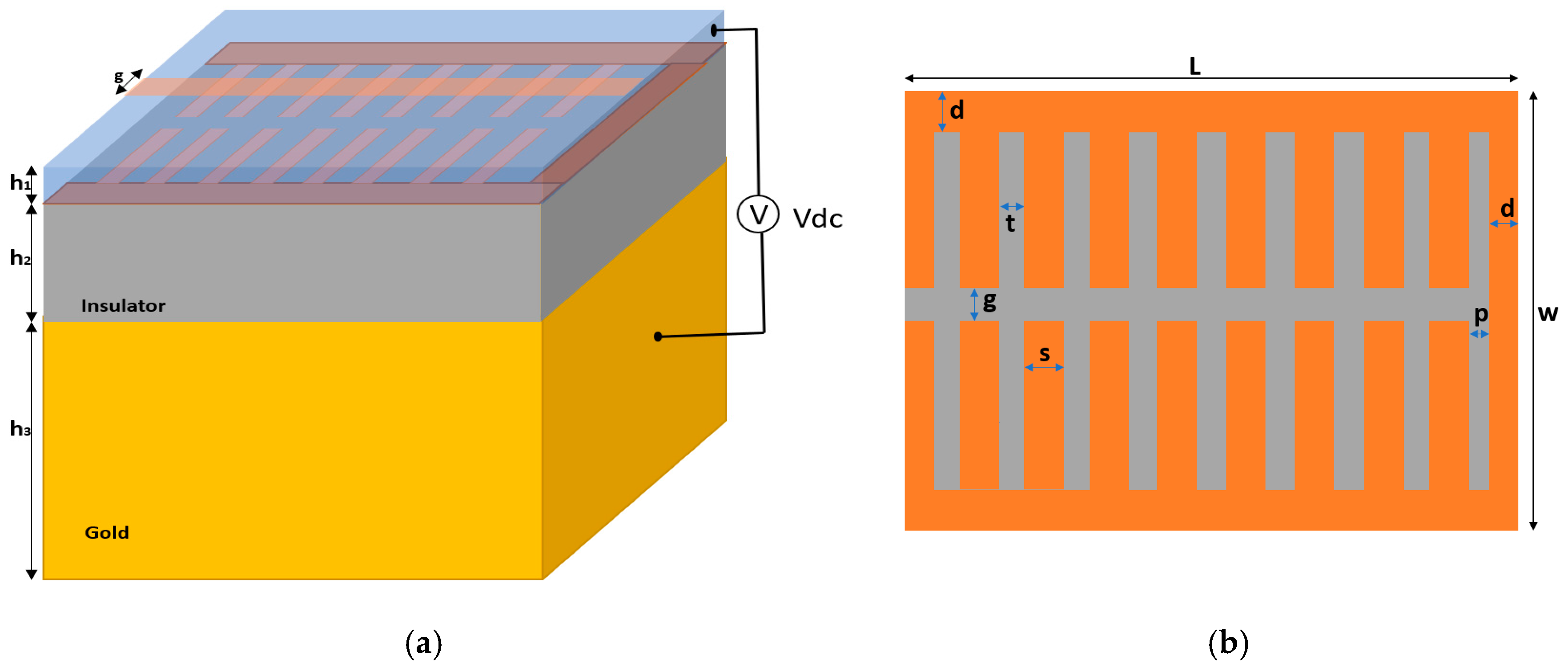
3. System Design
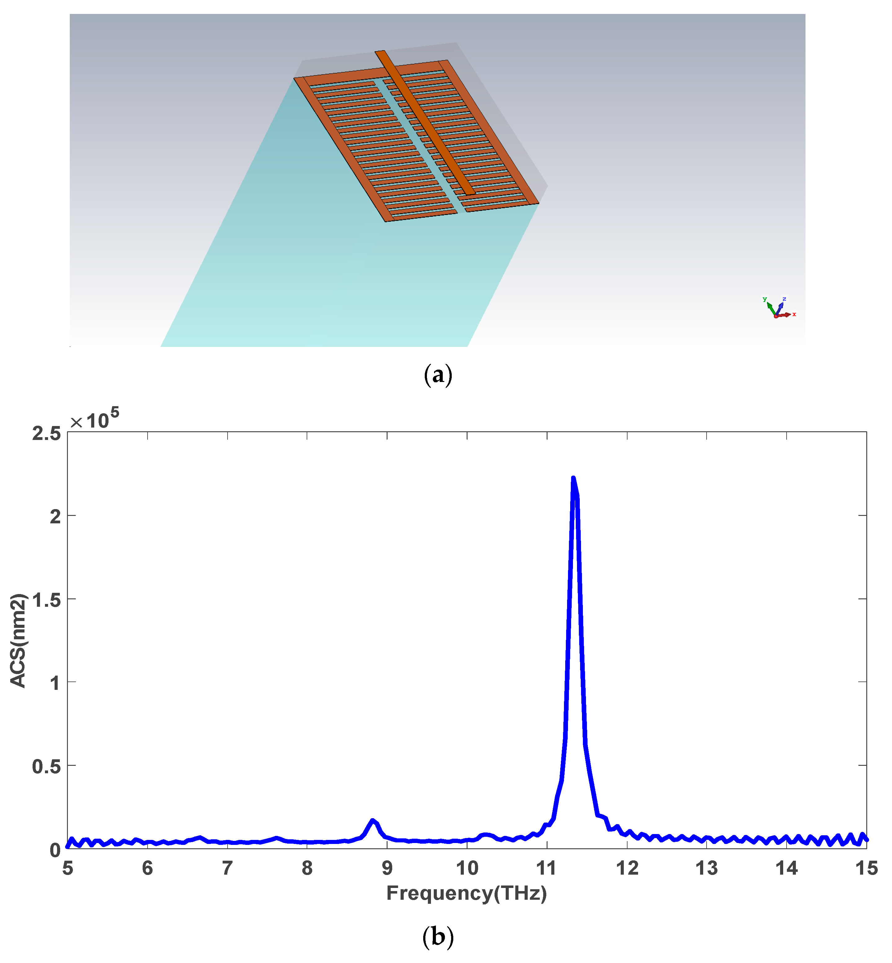
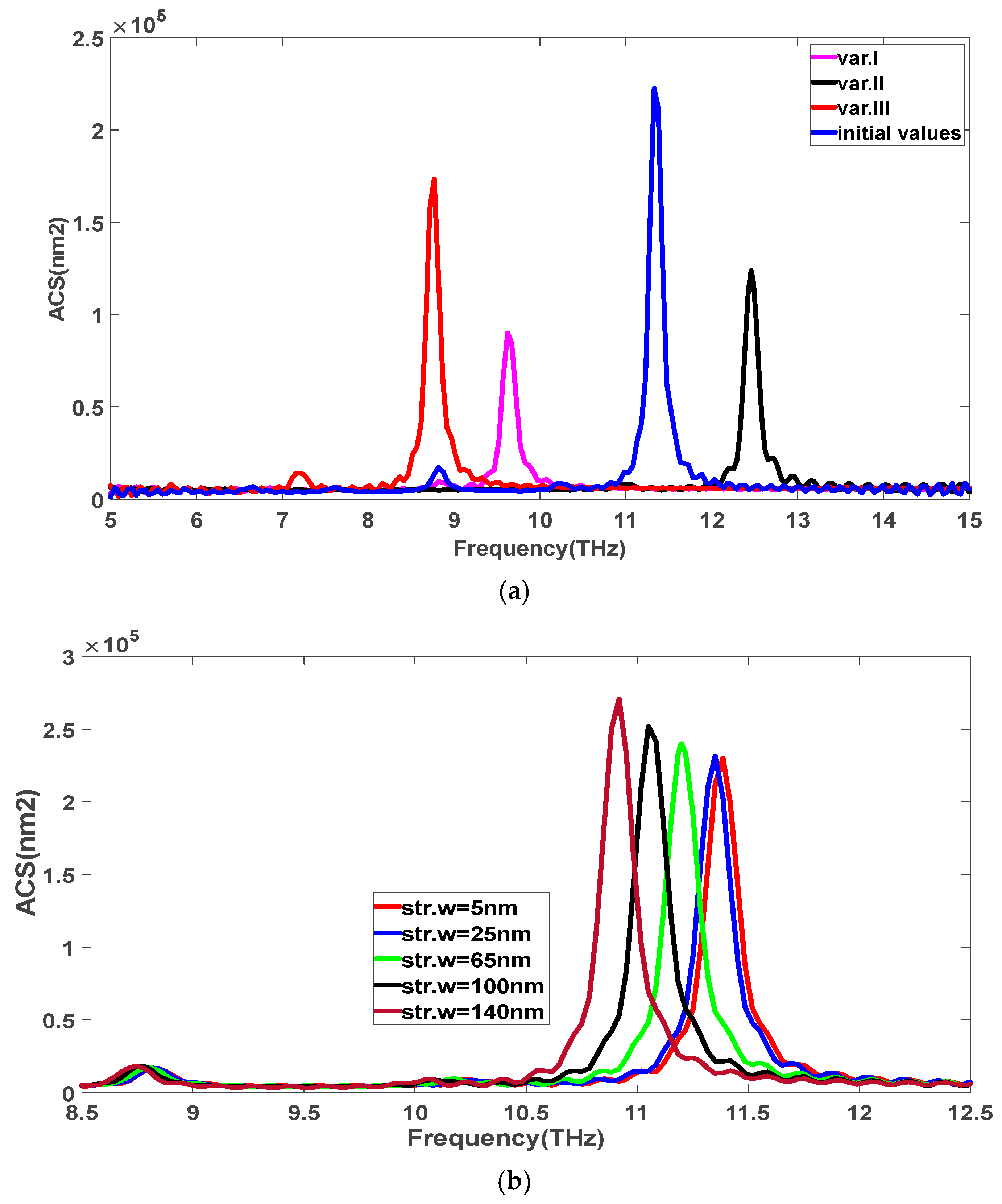
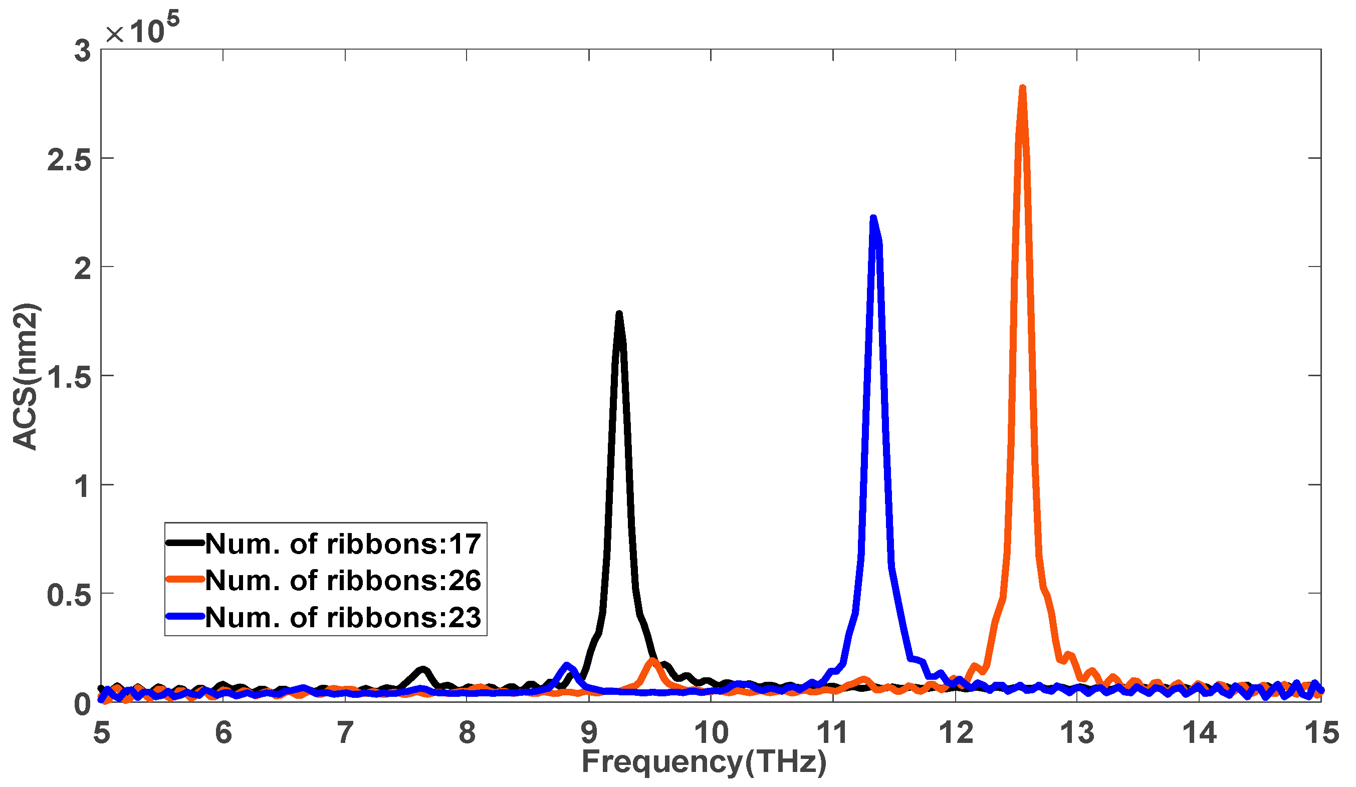
4. Simulation Results
5. Conclusions
Author Contributions
Funding
Institutional Review Board Statement
Informed Consent Statement
Data Availability Statement
Conflicts of Interest
References
- Banerjee, S.; Pal, B.P.; Roy Chowdhury, D. Resonance phenomena in electromagnetic metamaterials for the terahertz domain: A review. J. Electromagn. Waves Appl. 2020, 34, 1314–1337. [Google Scholar] [CrossRef]
- Xu, W.; Xie, L.; Ying, Y. Mechanisms and applications of terahertz metamaterial sensing: A review. Nanoscale 2017, 9, 13864–13878. [Google Scholar] [CrossRef]
- Nejat, M.; Nozhat, N. Sensing and switching capabilities of a tunable GST-based perfect absorber in near-infrared region. J. Phys. D Appl. Phys. 2020, 53, 245105. [Google Scholar] [CrossRef]
- Yi, Z.; Liang, C.; Chen, X.; Zhou, Z.; Tang, Y.; Ye, X.; Yi, Y.; Wang, J.; Wu, P. Dual-band plasmonic perfect absorber based on graphene metamaterials for refractive index sensing application. Micromachines 2019, 10, 443. [Google Scholar] [CrossRef] [Green Version]
- Grant, J.; Ma, Y.; Saha, S.; Khalid, A.; Cumming, D.R.S. Polarization insensitive, broadband terahertz metamaterial absorber. Opt. Lett. 2011, 36, 3476–3478. [Google Scholar] [CrossRef]
- Mao, Z.; Liu, S.; Bian, B.; Wang, B.; Ma, B.; Chen, L.; Xu, J. Multi-band polarization-insensitive metamaterial absorber based on Chinese ancient coin-shaped structures. J. Appl. Phys. 2014, 115, 204505. [Google Scholar] [CrossRef]
- Qiu Xu, Y.; Heng Zhou, P.; Bin Zhang, H.; Chen, L.; Jiang Deng, L. A wide-angle planar metamaterial absorber based on split ring resonator coupling. J. Appl. Phys. 2011, 110, 044102. [Google Scholar] [CrossRef]
- Zhao, J.; Yu, X.; Yang, X.; Th Tee, C.A.; Yuan, W.; Yu, Y. Polarization-independent and high-efficiency broadband optical absorber in visible light based on nanostructured germanium arrays. Opt. Lett. 2019, 44, 963–966. [Google Scholar] [CrossRef] [PubMed]
- Liao, Y.-L.; Zhao, Y. Ultra-narrowband dielectric metamaterial absorber with ultra-sparse nanowire grids for sensing applications. Sci. Rep. 2020, 10, 1480. [Google Scholar] [CrossRef] [PubMed] [Green Version]
- Lu, G.; Wu, F.; Zheng, M.; Chen, C.; Zhou, X.; Diao, C.; Liu, F.; Du, G.; Xue, C.; Jiang, H.; et al. Perfect optical absorbers in a wide range of incidence by photonic heterostructures containing layered hyperbolic metamaterials. Opt. Express 2019, 27, 5326–5336. [Google Scholar] [CrossRef] [PubMed]
- Gao, H.; Zhou, D.; Cui, W.; Liu, Z.; Liu, Y.; Jing, Z.; Peng, W. Ultraviolet broadband plasmonic absorber with dual visible and near-infrared narrow bands. J. Opt. Soc. Am. A 2019, 36, 264–269. [Google Scholar] [CrossRef]
- Nguyen, D.M.; Lee, D.; Rho, J. Control of light absorbance using plasmonic grating based perfect absorber at visible and near-infrared wavelengths. Sci. Rep. 2017, 7, 2611. [Google Scholar] [CrossRef] [Green Version]
- Xu, L.; Peng, B.; Luo, X.; Zhai, X.; Wang, L. A broadband and polarization-insensitive perfect absorber based on a van der Waals material in the mid-infrared regime. Results Phys. 2019, 15, 102687. [Google Scholar] [CrossRef]
- Wang, S.; Yu, H.; Zhang, H.; Wang, A.; Zhao, M.; Chen, Y.; Mei, L.; Wang, J. Broadband Few-Layer MoS2 Saturable Absorbers. Adv. Mater. 2014, 26, 3538–3544. [Google Scholar] [CrossRef] [PubMed]
- Jang, T.; Youn, H.; Shin, Y.J.; Guo, L.J. Transparent and Flexible Polarization-Independent Microwave Broadband Absorber. ACS Photonics 2014, 1, 279–284. [Google Scholar] [CrossRef]
- Zhang, Y.; Feng, Y.; Zhu, B.; Zhao, J.; Jiang, T. Graphene based tunable metamaterial absorber and polarization modulation in terahertz frequency. Opt. Express 2014, 22, 22743–22752. [Google Scholar] [CrossRef] [PubMed]
- Liu, N.; Mesch, M.; Weiss, T.; Hentschel, M.; Giessen, H. Infrared Perfect Absorber and Its Application as Plasmonic Sensor. Nano Lett. 2010, 10, 2342–2348. [Google Scholar] [CrossRef]
- Ghobadi, A.; Hajian, H.; Gokbayrak, M.; Dereshgi, S.A.; Toprak, A.; Butun, B.; Ozbay, E. Visible light nearly perfect absorber: An optimum unit cell arrangement for near absolute polarization insensitivity. Opt. Express 2017, 25, 27624–27634. [Google Scholar] [CrossRef]
- Gu, M.; Xiao, B.; Xiao, S. Tunable THz perfect absorber with two absorption peaks based on graphene microribbons. Micro Nano Lett. 2018, 13, 631–635. [Google Scholar] [CrossRef] [Green Version]
- Novoselov, K.S.; Geim, A.K.; Morozov, S.V.; Jiang, D.; Zhang, Y.; Dubonos, S.V.; Grigorieva, I.V.; Firsov, A.A. Electric Field Effect in Atomically Thin Carbon Films. Science 2004, 306, 666–669. [Google Scholar] [CrossRef] [Green Version]
- Geim, A.K.; Novoselov, K.S. The rise of graphene. Nat. Mater. 2007, 6, 183–191. [Google Scholar] [CrossRef] [PubMed]
- Wu, D.; Wang, M.; Feng, H.; Xu, Z.; Liu, Y.; Xia, F.; Zhang, K.; Kong, W.; Dong, L.; Yun, M. Independently tunable perfect absorber based on the plasmonic properties in double-layer graphene. Carbon 2019, 155, 618–623. [Google Scholar] [CrossRef]
- Lee, S.H.; Choi, M.; Kim, T.-T.; Lee, S.; Liu, M.; Yin, X.; Choi, H.K.; Lee, S.S.; Choi, C.-G.; Choi, S.-Y.; et al. Switching terahertz waves with gate-controlled active graphene metamaterials. Nat. Mater. 2012, 11, 936–941. [Google Scholar] [CrossRef] [Green Version]
- Valmorra, F.; Scalari, G.; Maissen, C.; Fu, W.; Schönenberger, C.; Choi, J.W.; Park, H.G.; Beck, M.; Faist, J. Low-Bias Active Control of Terahertz Waves by Coupling Large-Area CVD Graphene to a Terahertz Metamaterial. Nano Lett. 2013, 13, 3193–3198. [Google Scholar] [CrossRef] [PubMed]
- Yao, Y.; Shankar, R.; Kats, M.A.; Song, Y.; Kong, J.; Loncar, M.; Capasso, F. Electrically Tunable Metasurface Perfect Absorbers for Ultrathin Mid-Infrared Optical Modulators. Nano Lett. 2014, 14, 6526–6532. [Google Scholar] [CrossRef] [PubMed]
- Li, H.; Wang, L.; Zhai, X. Tunable graphene-based mid-infrared plasmonic wide-angle narrowband perfect absorber. Sci. Rep. 2016, 6, 36651. [Google Scholar] [CrossRef] [Green Version]
- Piper, J.R.; Fan, S. Total Absorption in a Graphene Monolayer in the Optical Regime by Critical Coupling with a Photonic Crystal Guided Resonance. ACS Photonics 2014, 1, 347–353. [Google Scholar] [CrossRef]
- Vorobev, A.S.; Bianco, G.V.; Bruno, G.; D’Orazio, A.; O’Faolain, L.; Grande, M. Tuning of Graphene-Based Optical Devices Operating in the Near-Infrared. Appl. Sci. 2021, 11, 8367. [Google Scholar] [CrossRef]
- Grande, M.; Bianco, G.V.; Perna, F.M.; Capriati, V.; Capezzuto, P.; Scalora, M.; Bruno, G.; D’Orazio, A. Reconfigurable and optically transparent microwave absorbers based on deep eutectic solvent-gated graphene. Sci. Rep. 2019, 9, 5463. [Google Scholar] [CrossRef]
- Balci, O.; Polat, E.O.; Kakenov, N.; Kocabas, C. Graphene-enabled electrically switchable radar-absorbing surfaces. Nat. Commun. 2015, 6, 6628. [Google Scholar] [CrossRef] [Green Version]
- Yao, H.; Wang, C.; Zaki, K.A. Effects of tuning structures on combline filters. In Proceedings of the 1996 26th European Microwave Conference, Prague, Czech Republic, 6–13 September 1996; pp. 427–430. [Google Scholar]
- Awai, I. Design of Multistage Combline Band-Pass Filters in Layered Structures. In Novel Technologies for Microwave and Millimeter—Wave Applications; Kiang, J.-F., Ed.; Springer: Boston, MA, USA, 2004; pp. 83–100. [Google Scholar]
- Andryieuski, A.; Lavrinenko, A.V. Graphene metamaterials based tunable terahertz absorber: Effective surface conductivity approach. Opt. Express 2013, 21, 9144–9155. [Google Scholar] [CrossRef] [Green Version]
- Yao, Y.; Kats, M.A.; Genevet, P.; Yu, N.; Song, Y.; Kong, J.; Capasso, F. Broad Electrical Tuning of Graphene-Loaded Plasmonic Antennas. Nano Lett. 2013, 13, 1257–1264. [Google Scholar] [CrossRef] [PubMed]
- Zhang, Y.; Li, T.; Chen, Q.; Zhang, H.; O’Hara, J.F.; Abele, E.; Taylor, A.J.; Chen, H.-T.; Azad, A.K. Independently tunable dual-band perfect absorber based on graphene at mid-infrared frequencies. Sci. Rep. 2015, 5, 18463. [Google Scholar] [CrossRef] [Green Version]
- Gómez-Díaz, J.S.; Perruisseau-Carrier, J. Graphene-based plasmonic switches at near infrared frequencies. Opt. Express 2013, 21, 15490–15504. [Google Scholar] [CrossRef] [PubMed] [Green Version]
- Zhang, J.; Zhu, Z.; Liu, W.; Yuan, X.; Qin, S. Towards photodetection with high efficiency and tunable spectral selectivity: Graphene plasmonics for light trapping and absorption engineering. Nanoscale 2015, 7, 13530–13536. [Google Scholar] [CrossRef]
- Wang, X.; Shi, Y. CHAPTER 1 Fabrication Techniques of Graphene Nanostructures. In Nanofabrication and Its Application in Renewable Energy; The Royal Society of Chemistry: Cambridge, UK, 2014; pp. 1–30. [Google Scholar]
- Nguyen, B.-S.; Lin, J.-F.; Perng, D.-C. 1-nm-thick graphene tri-layer as the ultimate copper diffusion barrier. Appl. Phys. Lett. 2014, 104, 082105. [Google Scholar] [CrossRef]
- Dash, S.; Patnaik, A. Performance of Graphene Plasmonic Antenna in Comparison with Their Counterparts for Low-Terahertz Applications. Plasmonics 2018, 13, 2353–2360. [Google Scholar] [CrossRef]
- Bohren, C.F.; Huffman, D.R. Absorption and Scattering of Light by Small Particles; John Wiley & Sons: Hoboken, NJ, USA, 2008. [Google Scholar]
- Ullah, Z.; Witjaksono, G.; Nawi, I.; Tansu, N.; Irfan Khattak, M.; Junaid, M. A Review on the Development of Tunable Graphene Nanoantennas for Terahertz Optoelectronic and Plasmonic Applications. Sensors 2020, 20, 1401. [Google Scholar] [CrossRef] [PubMed] [Green Version]
- Cen, C.; Chen, Z.; Xu, D.; Jiang, L.; Chen, X.; Yi, Z.; Wu, P.; Li, G.; Yi, Y. High Quality Factor, High Sensitivity Metamaterial Graphene—Perfect Absorber Based on Critical Coupling Theory and Impedance Matching. Nanomaterials 2020, 10, 95. [Google Scholar] [CrossRef] [PubMed] [Green Version]
- Bott, A.W. Electrochemistry of semiconductors. Curr. Sep. 1998, 17, 87–92. [Google Scholar]
- Stoliar, P.; Calò, A.; Valle, F.; Biscarini, F. Fabrication of Fractal Surfaces by Electron Beam Lithography. IEEE Trans. Nanotechnol. 2010, 9, 229–236. [Google Scholar] [CrossRef]
- Nur, O.; Willander, M. (Eds.) Chapter 3—Conventional nanofabrication methods. In Low Temperature Chemical Nanofabrication; William Andrew Publishing: Norrköping, Sweden, 2020; pp. 49–86. [Google Scholar]


| Parameter | p (nm) | s (nm) | d (nm) | t (nm) | G (nm) | L (nm) | W (nm) |
|---|---|---|---|---|---|---|---|
| Size value | 7.5 | 10 | 25 | 6.25 | 25 | 400 | 400 |
| Geometric Specification | s (nm) | t (nm) | p (nm) |
|---|---|---|---|
| Variation.I | 8 | 8.25 | 9.5 |
| Variation.II | 12 | 4.5 | 7.5 |
| Variation.III | 6 | 10.25 | 11.5 |
| Geometric Specification | Plasmonic Resonant Frequency (THz) | Absorption Intensity (×105 nm2) |
|---|---|---|
| Initial size | 11.348 | 2.366 |
| Variation I | 8.77 | 1.732 |
| Variation II | 9.622 | 0.9014 |
| Variation III | 12.456 | 1.24 |
| The Width of Graphene Stripline (nm) | Plasmonic Resonant Frequency (THz) | Absorption Intensity (×105 nm2) |
|---|---|---|
| 5 | 11.386 | 2.299 |
| 25 | 11.346 | 2.366 |
| 65 | 11.2 | 2.4 |
| 100 | 11.052 | 2.521 |
| 140 | 10.92 | 2.704 |
| The Number of Ribbon Teeth | Plasmonic Resonant Frequency (THz) | Absorption Intensity (×105 nm2) |
|---|---|---|
| N = 17 | 9.246 | 1.784 |
| N = 23 | 11.346 | 2.366 |
| N = 26 | 12.556 | 2.823 |
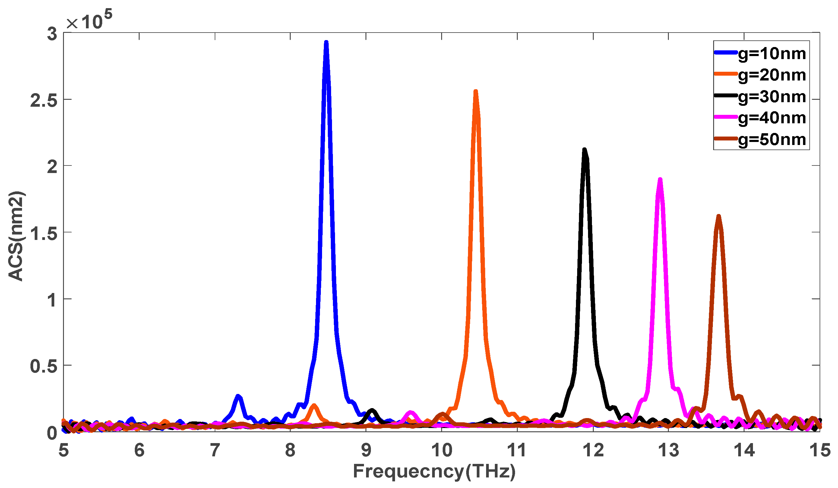
| g-Distance (nm) | Plasmonic Resonant Frequency (THz) | Absorption Intensity (×105 nm2) |
|---|---|---|
| 10 | 8.477 | 2.929 |
| 20 | 10.45 | 2.56 |
| 25 | 11.348 | 2.366 |
| 30 | 11.89 | 2.122 |
| 40 | 12.891 | 1.899 |
| 50 | 13.66 | 1.822 |
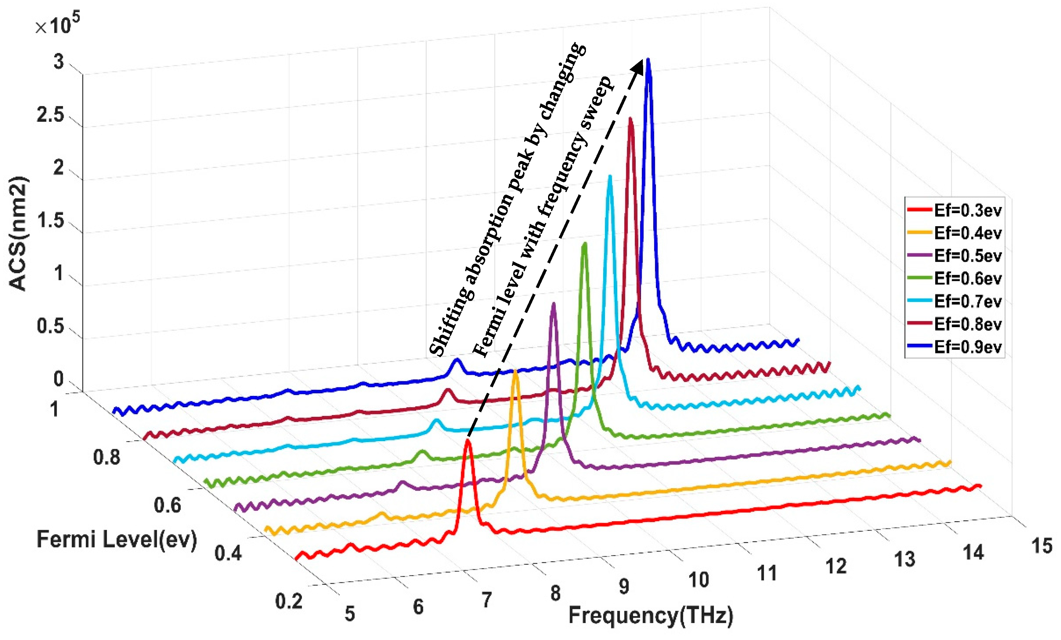
| Fermi Potential (eV) | 0.4 | 0.5 | 0.6 | 0.7 | 0.8 | 0.9 |
| Plasmonic resonant frequency(THz) | 8.644 | 9.647 | 10.55 | 11.353 | 12.09 | 12.79 |
| Amplitude of absorption peak(×105 nm2) | 1.3285 | 1.671 | 1.959 | 2.314 | 2.584 | 2.871 |
Publisher’s Note: MDPI stays neutral with regard to jurisdictional claims in published maps and institutional affiliations. |
© 2021 by the authors. Licensee MDPI, Basel, Switzerland. This article is an open access article distributed under the terms and conditions of the Creative Commons Attribution (CC BY) license (https://creativecommons.org/licenses/by/4.0/).
Share and Cite
Maghoul, A.; Rostami, A.; Barzinjy, A.A.; Mirtaheri, P. Electrically Tunable Perfect Terahertz Absorber Using Embedded Combline Graphene Layer. Appl. Sci. 2021, 11, 10961. https://doi.org/10.3390/app112210961
Maghoul A, Rostami A, Barzinjy AA, Mirtaheri P. Electrically Tunable Perfect Terahertz Absorber Using Embedded Combline Graphene Layer. Applied Sciences. 2021; 11(22):10961. https://doi.org/10.3390/app112210961
Chicago/Turabian StyleMaghoul, Amir, Ali Rostami, Azeez Abdullah Barzinjy, and Peyman Mirtaheri. 2021. "Electrically Tunable Perfect Terahertz Absorber Using Embedded Combline Graphene Layer" Applied Sciences 11, no. 22: 10961. https://doi.org/10.3390/app112210961
APA StyleMaghoul, A., Rostami, A., Barzinjy, A. A., & Mirtaheri, P. (2021). Electrically Tunable Perfect Terahertz Absorber Using Embedded Combline Graphene Layer. Applied Sciences, 11(22), 10961. https://doi.org/10.3390/app112210961