1. Introduction
The problem of poor power quality in power systems normally results from the extensive use and integration of renewable energy systems or resources, adverse loading, or the use of a non-linear load at an extensive level. This problem may include voltage fluctuation, imbalance of the voltage in the three-phase system, voltage sags and swells, etc. Among these problems, the voltage sags and swells are critical for loads that are very sensitive to voltage variation. These issues may lead to the missed or incorrect operation of sensitive electronic devices or equipment. To address these issues, the use of flexible AC transmission (FACTS) controllers may offer a possible solution if they are employed as a dynamic voltage restorer (DVR) [
1,
2,
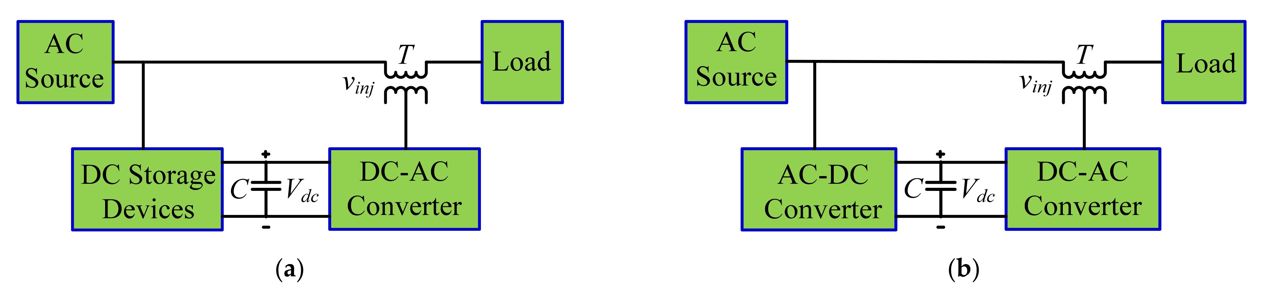
3]. The basic principle of protection in these devices is the series injection of voltage between the load and point of common coupling (source or transformer) in the power system. The DVRs may be employed in a DC-link-based system, as shown in
Figure 1. The most commonly used configuration of DVR, as illustrated in [
4,
5,
6], is depicted in
Figure 1a, which is based on the use of a voltage source inverter and voltage injection transformer connected in series with the line. The input power of these types of DVRs is taken from DC energy-storing devices such as batteries. The duration of the compensation voltage in these configurations depends on the size and capacity of the energy-storing devices but cannot support longer-duration voltage variations. This issue is addressed and tackled in other configurations for voltage compensation [
7,
8], as shown in
Figure 1b. Here, a front-side AC-DC converter eliminates the use of energy-storing devices, enabling the compensator to deal with the longer-duration problems. In both previously discussed configurations, the use of a bulky DC-link capacitor is mandatory, which has very severe reliability issues. Therefore, these configurations are not suitable for applications where only voltage stabilization is required.
In the other developed approaches of DVRs, the stabilization of the required voltage may be ensured by the PWM control of the direct AC-AC converters [
9]. These configurations eliminate the use of a DC-link capacitor; hence, this improves the overall system’s reliability. Direct AC-AC topologies may be realized with a Z-source structure [
10,
11,
12,
13,
14] to increase the capability of the voltage transfer ratio. This also eliminates the risk of short-circuit problems or the paralleling of capacitors connected to input and output terminals. These problems may result from the turning on of the switching transistors connected in series, which must be operated in a complementary way. The usage of a number of passive elements and operating devices is a serious challenge in these power-converting approaches, which is the main cause of their large overall size and cost. The presence of the high-order elements in this arrangement also seriously impacts the dynamic response. There is also an issue of high current stresses conducted in the switching devices during the shoot-through intervals, which increase their power rating, resulting in high costs. These issues are tackled in power-converting approaches implemented without a Z-source configuration, as reported in [
15,
16,
17,
18,
19,
20]. In these power-converting topologies, an inductor at the intermediate level is employed for energy storage and to avoid the shoot-through issue. The bidirectional current conduction capabilities of the switching MOSFETs in converters [
15,
17,
18,
19,
20] are forced to be unidirectional by connecting a fast recovery at the source end. This arrangement always ensures the reverse biasing or blocking of the conduction of the MOSFET’s body diode. This approach not only avoids the shoot-through problem but also simplifies the circuit configuration as well as the switching control techniques. The power quality validation of the AC voltage controllers realized with the direct approach of AC power conversion topologies is explored in [
16]. Therefore, these converters are well-suited for the voltage stabilization of a sensitive load in the case of voltage fluctuation.
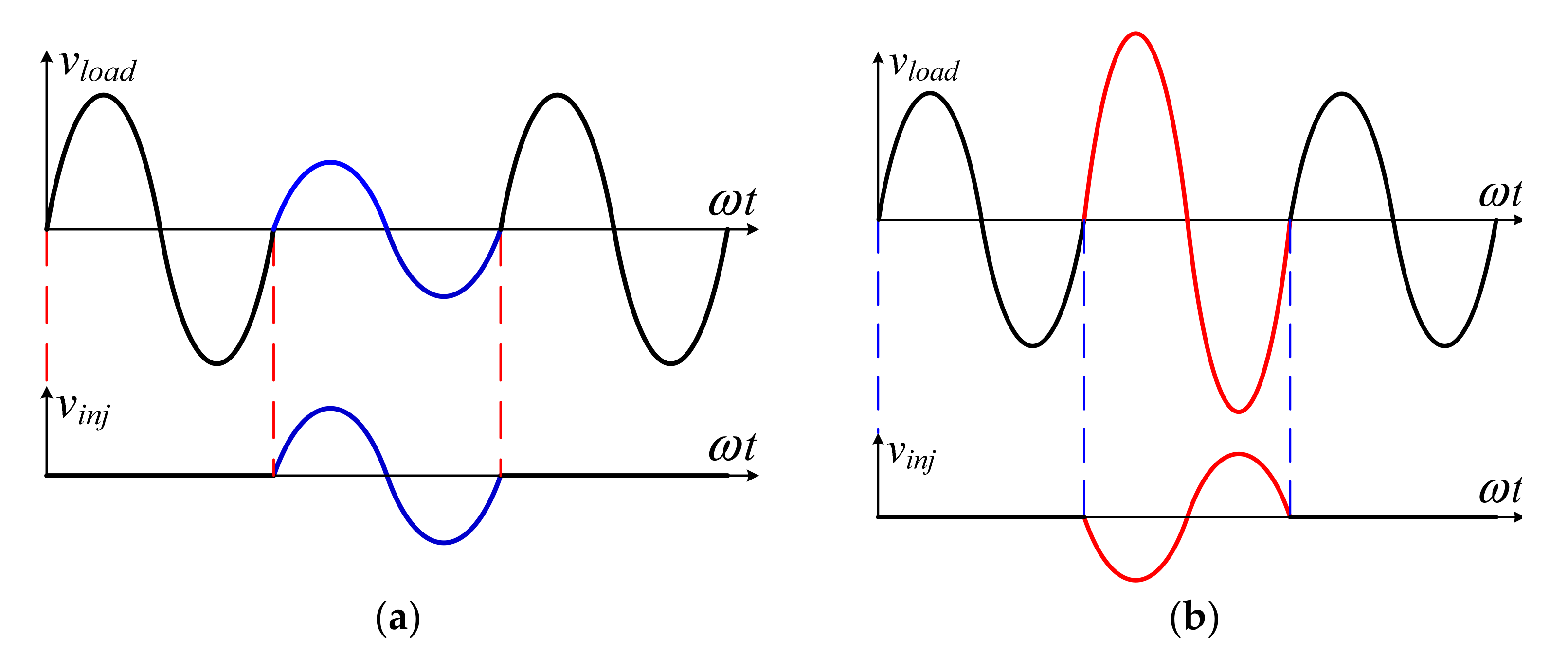
For low-voltage issues, the rms value of the line voltage is dropped approximately to 80% to 20% of its rated rms values. Thus, to tackle the load voltage, a compensation voltage is added to the line voltage, as shown in
Figure 2a. This can only be realized if the output voltage of a DVR is in phase with the input phase voltage. Therefore, an AC-AC converter has to be operated in non-inverting mode. In the same way, during the voltage swell issue, the line or load rms voltage is increased to 120 to 180% of its rated value. In this case, the compensator’s voltage is to be subtracted from the line voltage to stabilize them, as may be seen in
Figure 2b. Thus, the required operating mode of the AC-AC compensator employed in DVR is inverting. Consequently, a variable bipolar voltage gain is required to tackle the issues of voltage sag and swell.
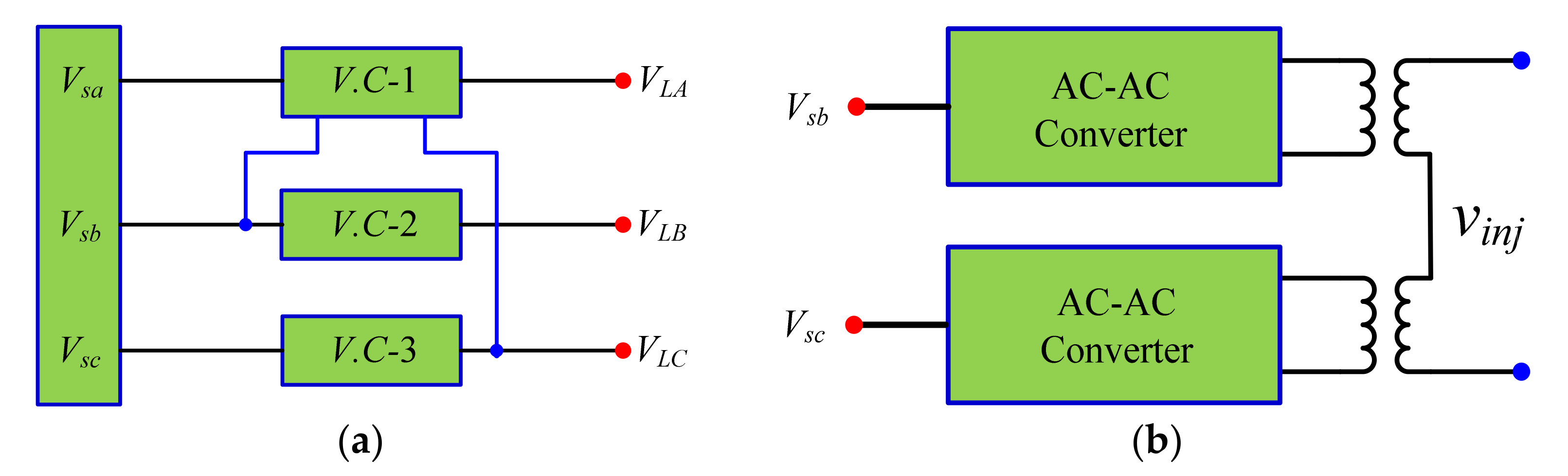
The input of the AC voltage controllers present in the DVRs employed in a three-phase system may be connected in the healthy phases rather than the faulty phase. One such approach is called the interphase technique, developed in [
21], which is shown in
Figure 3a. The DVR connected in the faulty phase consists of two AC voltage controllers, as depicted in
Figure 3b. The input of one AC voltage controller is connected to one of the non-faulty phases, while the input of the other one is taken from the other healthy phase. For example, the inputs of voltage compensator 1 connected in phase ‘
a’ are connected to phase ‘
b’ and ‘
c’, as can be seen in
Figure 3a,b. The outputs of these two AC voltage controllers are not only out of phase with respect to each other but are also not aligned with the phase voltage of the faulty line [
21]. Here, the voltage injection in the faulty phase is a challenging issue. This problem is tackled by adding the outputs of the two AC voltage controllers through the series connection of two transformers. The resulting output voltage of this setup has two components, where one component is in phase with the voltage of the faulty phase, but the other component is quadrature with respect to this phase. The second component of the injected voltage is unwanted and its value is made zero with the adjustment of the duty cycles of the controllers. Therefore, adjusting the voltage gain of the desired component with the cancelation of the quadrature component is a very challenging issue. Moreover, the use of the two series voltage injection transformers and two AC voltage controllers increases the overall size, cost, and losses.
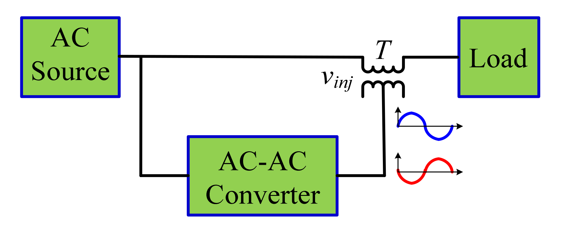
These issues may be tackled if the AC voltage controller connected in the faulty phase takes the input power from the same phase where it is connected. This approach is depicted in
Figure 4, ensuring the use of a single AC-AC converter with a line frequency transformer for voltage injection. The overall arrangement lowers the size and cost of the DVR. However, with this configuration, the value of the required voltage gains for the problem of voltage sag or swell has a high depth level, normally more than one. This necessitates the development of a converter that may invert or non-invert output with voltage step-up capabilities.
The voltage stabilization features may also be obtained with buck-boost controllers. There is a power quality issue associated with the input current as it is discontinuous. High conversion losses result from high values of the switching current and voltage. The discontinuity in the input current is tackled in [
22,
23,
24] by adding more passive components and semiconductor devices. This may result in high costs and conversion losses due to the conduction of a large number of components and switching devices.
Applications such as line voltage correction having a high depth level or high-voltage-gain AC-to-DC converters need a high bipolar voltage gain. The required features of the voltage gain can be obtained with the realization of voltage boost voltage controllers, which are capable of non-inverting or inverting the input voltage at the output with voltage-regulated characteristics. One of the latest AC voltage controllers having bipolar voltage boost features is employed in [
20], as can be viewed in
Figure 5.
However, its realization requires the use of six switching transistors and eight diodes. The overall size and cost of any AC voltage controller are directly affected by the use of a number of switching transistors. The switching of one transistor requires the use of one gate-controlling circuit (GCC) with a separate isolated DC source (IDS). The size and cost of a GCC and IDS are much larger than those of a transistor or power converter circuit. The similar existing topologies use a large number of switching transistors (and associated circuits that deal with their turn-on and turn-off control) and diodes, which are the major sources of the increased overall volume, losses, and costs.
Therefore, in this article, a new boost voltage controller having bipolar voltage boost features is proposed that is realized with the use of six diodes and four switching transistors. Therefore, eliminating the number of switching transistors drastically reduces the overall size and cost of the converter. This circuit topology also helps to simplify the switching arrangements, and it also avoids the problems caused by the shoot-through. There is no possibility of interruption of the inductor current that may result from some inherent delay or defect in the operation of the switching transistors. For this purpose, an inductor is connected at the intermediate level to avoid paralleling the input and output capacitors or the shorting of the input or output capacitors. In the same way, the series connection of diode D5 with transistor Q4 and diode D6 with transistor Q2 helps to tackle the current interruption of the inductor current, which may otherwise lead to the generation of high inductive voltage kicks. With this approach, the transistor Q2 is ensured to be on for the positive input voltage once the transistor Q4 operates with high-frequency PWM control. Once the transistor Q4 is on, the transistor Q2 is also on, but it is in the non-conducting state as its series-connected diode is reverse-biased. This diode changes its state from off to on as transistor Q4 turns off. Thus, the inductor current remains uninterrupted for the PWM switching control for the transistor Q4. This is also true for the PWM switching control of the transistor Q2 as well.
The section-wise arrangement of this research article includes the demonstration of all operating modes in
Section 2 with the help of power transfer loops and control signals. The effectiveness of the proposed circuit is proven in
Section 3 through a comparison with topologies realized with similar strategies. The operational validation of the suggested circuit is carried out in
Section 4 with the comparison of results gained from computer software and a practical model. The conclusions are presented in
Section 5.
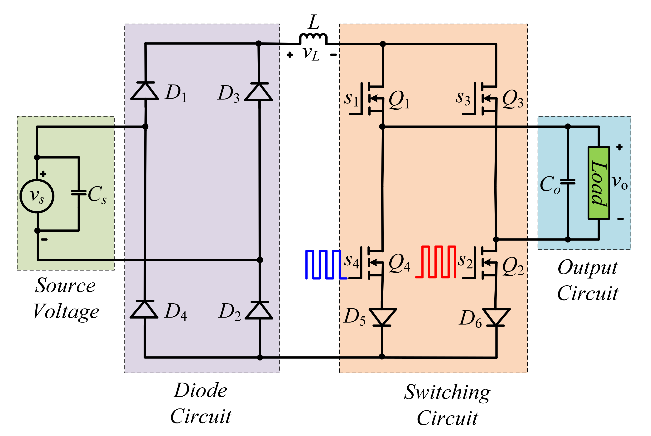
2. Proposed Circuit and Operating Modes
The circuit arrangement of the suggested topology is illustrated in
Figure 6. This circuit is a modified form of our developed frequency step-up controller, which is discussed in [
25]. The realization of the proposed circuit is achieved with the usage of six fast recovery diodes (
D1 to
D6) and four high switching transistors (
Q1 to
Q4). The switching transistors
Q1 and
Q3 operate at a low frequency (output or input frequency) while transistors
Q2 and
Q4 operate at a high switching frequency (in the kilohertz range). The power quality of the source and load sides is ensured by employing input and output capacitors. The inductor between the diodes and transistor circuits acts not only as a filtering or energy-storing element but also eliminates the possible shorting of the input or output capacitors. It also avoids the paralleling of the input and output capacitors. Therefore, the problem of possible shoot-through that may develop due to inherent turn-off delays of the high-frequency switching transistors is solved. For example, switching transistors
Q1 and
Q4 are connected in series and may operate in a complementary way. There is the possibility that
Q4 may turn on before the
Q1 turns off. In this case, the series-connected inductor (
L) prevents the short-circuiting of the input source. The same is also true for transistors
Q3 and
Q4. The current through the series inductor is always unidirectional, and its interruption is avoided with a proper control arrangement developed for the switching of the four transistors. In the same way, the possible shorting of the output capacitor (
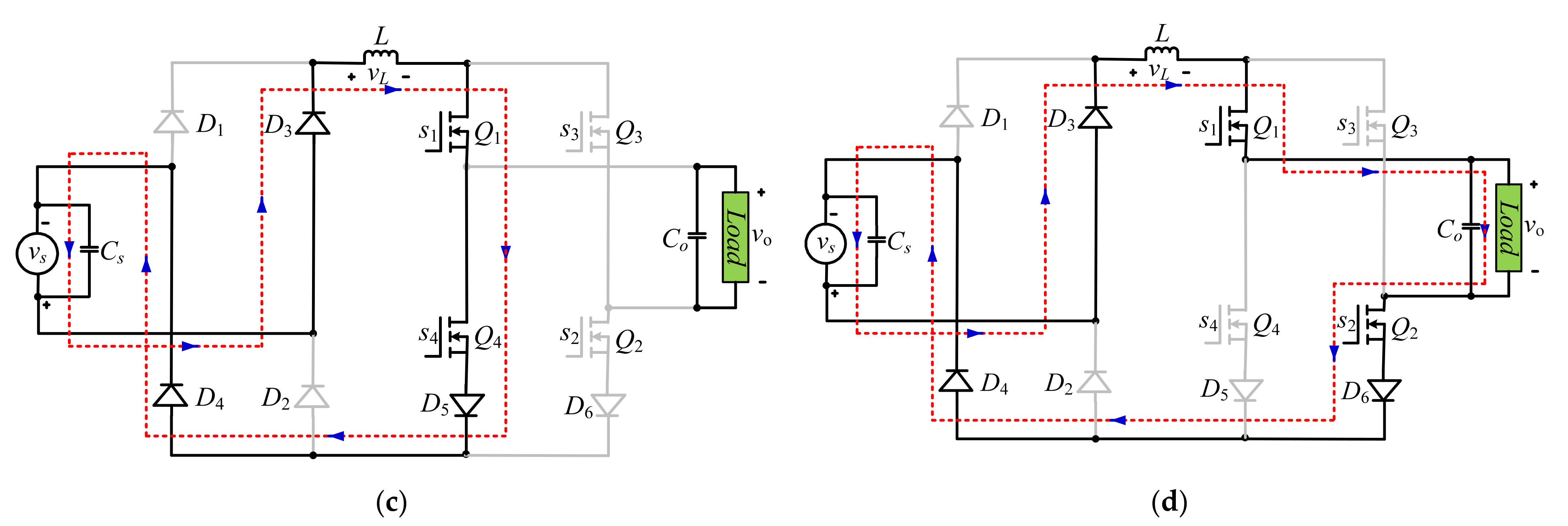
Co) is eliminated by connecting the diode
D5 in series with transistor
Q4 and diode
D6 in series with transistor
Q2. This connection arrangement ensures the reverse blocking of the body diodes of the switching transistors
Q4 and
Q2. There is no need to connect the series diodes with switching transistor
Q1 and
Q3 to ensure the reverse biasing of their body diodes. Here, the polarity of the output capacitor will perform this task. For example, once the switching transistor
Q1 is on and
Q3 is off, the negative terminal of the output capacitor is connected to the anode of the body diode of the switching transistor
Q3. The same is also true once the switching transistor
Q3 is on and transistor
Q1 is off. The suggested topology and its non-inverting and inverting voltage boost capabilities are detailed in the next section with the help of voltage control schemes and power transfer loops.
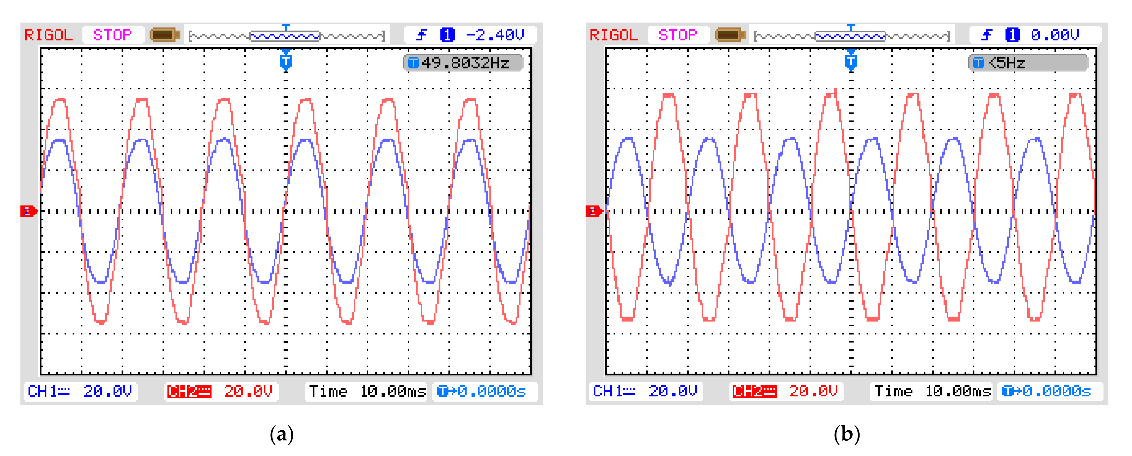
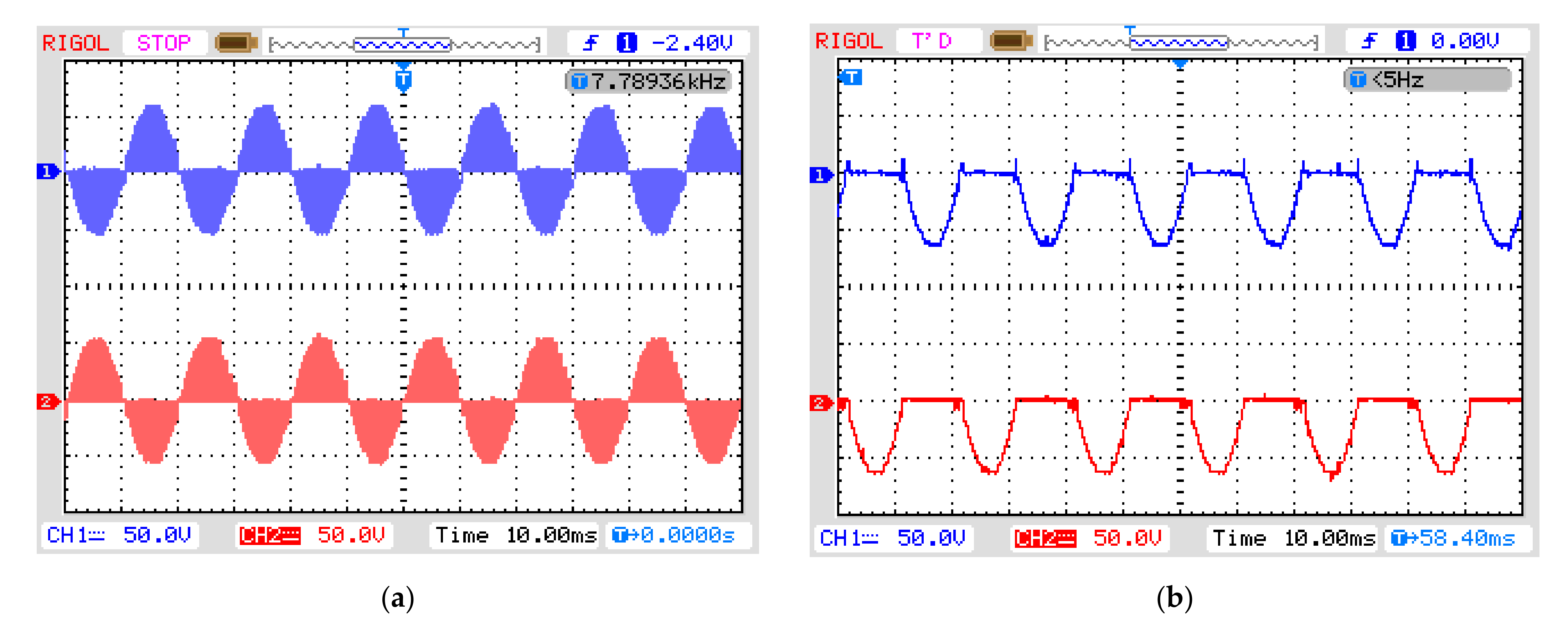
The regulated non-inverted and inverted output voltage is a mandatory requirement for stabilizing the load voltage during the problem of voltage sag and swell. The voltage of the output compensator must be added and subtracted from the load voltage in the event of voltage sag and swell issues, respectively. This requires non-inverting and inverting outputs with voltage-regulated characteristics. The diode bridge converts the sinusoidal input to its absolute form, while the transistor bridge ensures the regulated sinusoidal voltage at the output. The required regulated AC output is ensured with the switching of four transistors (Q1 to Q4). The inductor (L) and output capacitor (Co) are passive energy-storing elements, so they may be employed as state variables to explore the dynamic behavior.
2.1. Voltage Control with Non-Inverting Characteristics
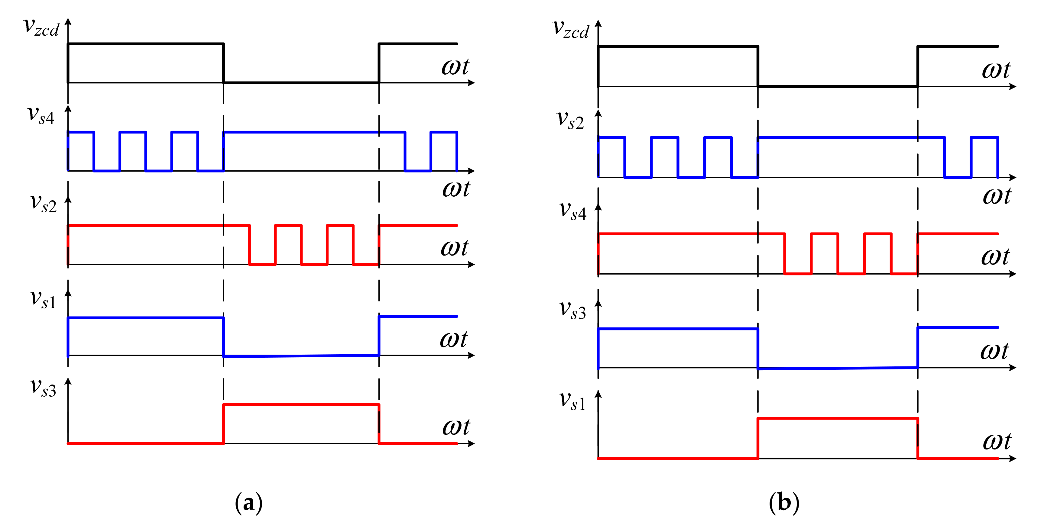
In this mode, the regulated voltage with boost characteristics and input voltage are in phase with each other. This output voltage feature may be ensured with control algorithms, as shown in
Figure 7a. In this figure,
vzcd is the output of a voltage-sensing circuit that detects the polarity of the input voltage. This voltage is logically high and low once the input voltage waveform passes through the positive and negative cross-over points, respectively. This is applied to the signal generator (microcontroller) as input; thus, all the control outputs of the signal generator are synchronized or aligned with the grid AC voltage. The control voltages
vs1 and
vs3 ensure the on states of the switching transistors
Q1 and
Q3 once the input voltage has positive and negative values. Similarly, the control voltage
vs4 and
vs2 are high-frequency PWM signals that switch transistors
Q4 and
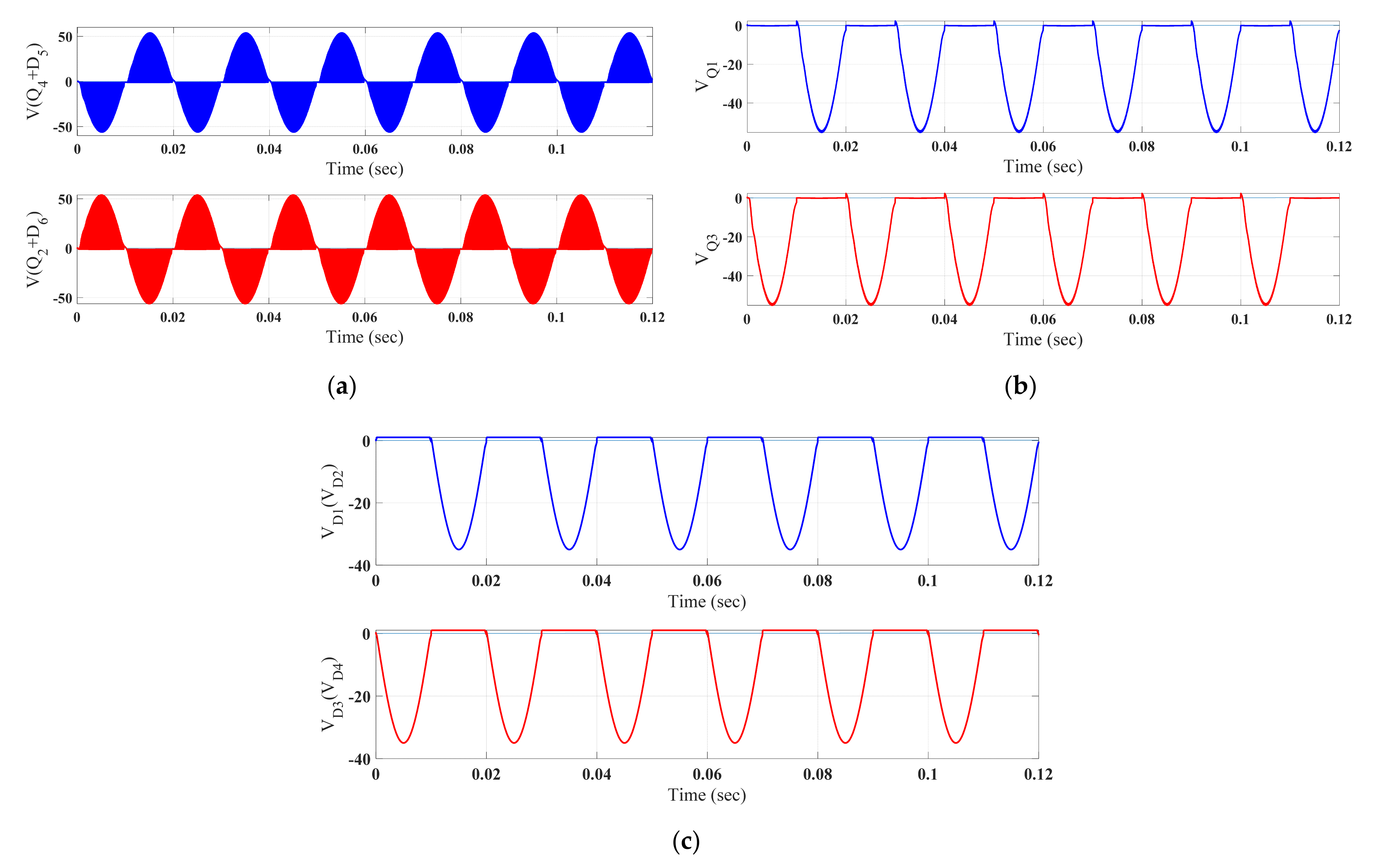
Q2, respectively. These control signals operate the switching transistors in a pulse width modulation (PWM) manner when the input voltage is positive and negative, respectively, to stabilize the output according to the requirement. The maximum off-state voltage across the turned-off switching transistors (
Q1 to
Q4) is restricted to the peak value of the output voltage.
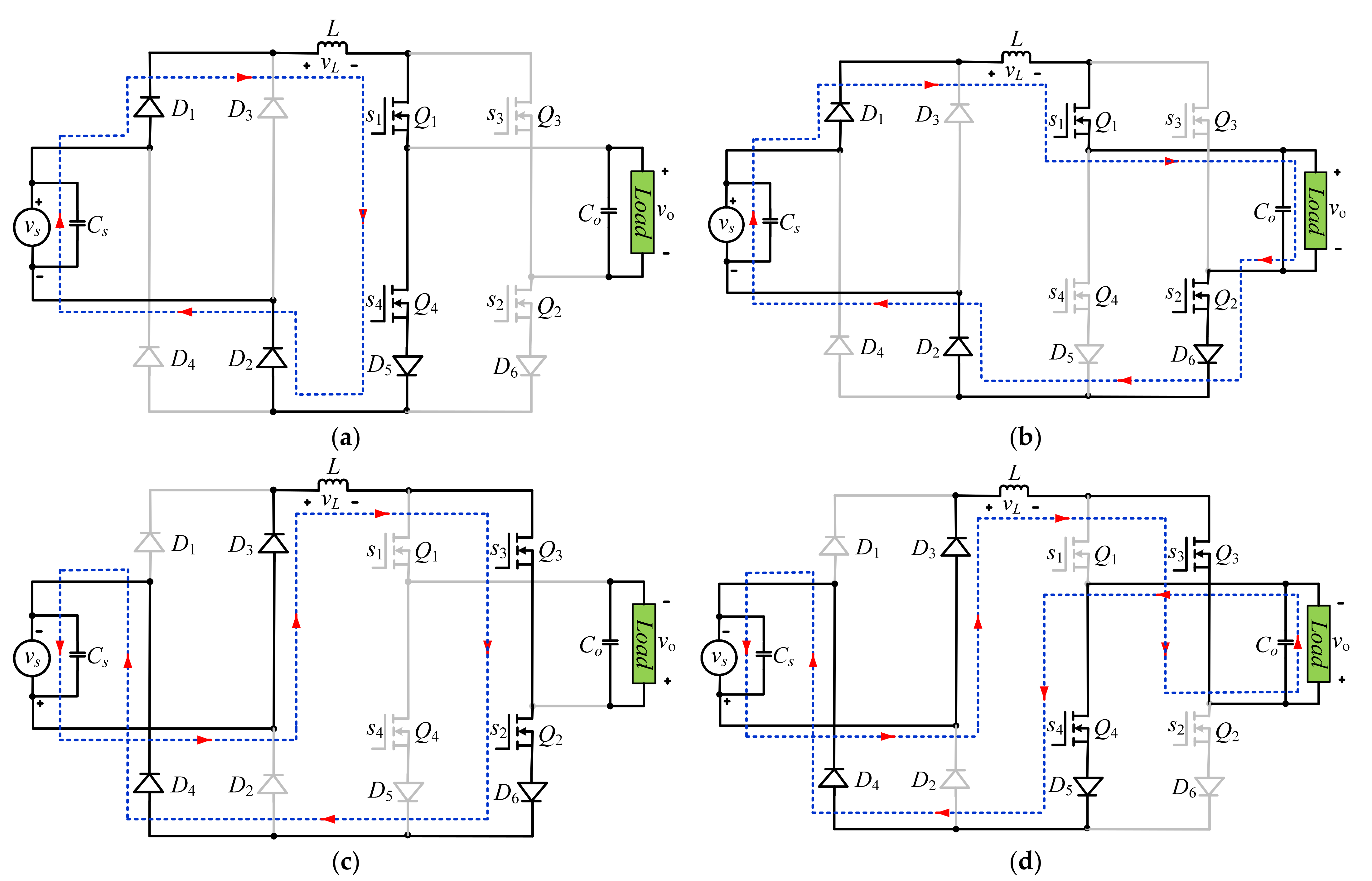
The details of the power transfer from input to output are explored in the highlighted loops of
Figure 8a–d when the value of the input is positive and negative, respectively.
For a positive input voltage, the diodes
D1 and
D2 are forward-biased, and the switching transistor
Q1 is on. The PWM switching of transistor
Q4 during the time interval ‘
kT’, stores the input power in inductor ‘
L’ through the current loop formed by the diodes
D1,
D2, and
D5 and switching transistors
Q1 and
Q4, as shown in
Figure 8a. Here, ‘
k’ and ‘
T’ are the pulse width and switching period of the high-frequency PWM control signal, respectively. The peak reverse voltage across the reverse-biased diodes (
D3 and
D4) of the diode bridge is equal to the peak value of the input voltage.
Similarly, the maximum reverse voltage across the
Q3 and
D6 is the peak output voltage.
In the ‘
kT’ interval, although the switching transistor
Q2 is on, it is in the non-conducting state as its series-connected diode
D6 is reverse-biased due to the polarity of the output capacitor. This transistor is maintained in conduction mode to eliminate the possible interruption of the inductor’s current as diode
D6 becomes forward once the switching transistor
Q4 turns off in the ‘(1 −
k)
T’ interval. During this interval, the stored power in the inductor is forwarded to the output through the power transfer loop highlighted in
Figure 8b. The maximum voltage across the series-connected switching transistor
Q4 and diode
D5 is
Vo(P).
During the negative half-cycle of the input voltage, the operating states of diodes
D3 and
D4 are changed from off to on and diodes
D1 and
D2 become reverse-biased with a break-over value of peak input voltage. The operating transistor
Q3 conducts, and
Q1 remains reverse-biased. Its value cannot exceed the maximum output voltage level during the entire negative half-cycle of the input voltage. The regulation of the output voltage is ensured with the PWM control of the switching transistor
Q2. The voltage across the non-conducting devices can be described as follows:
In the same voltage half-cycle, the turning on of the switching transistor
Q4 ensures the continuous inductor current as non-conducting diode
D5 that is connected in its series changes its operating state once the high-frequency PWM-controlled transistor
Q2 changes its switching state from ‘on’ to ‘off’. During a PWM interval, the transfer of power from the source to the inductor and then to output is shown in
Figure 8c,d, respectively. The dynamic variation in the inductor voltage and capacitor current is computed by employing Kirchhoff’s voltage law (KVL) for the inductor voltage and Kirchhoff’s current law (KCL) for the capacitor current, respectively. The inductor voltage and the capacitor current during the turn-on PWM intervals for any value of the supplied voltage are expressed by
The inductor voltage and capacitor current during the turn-off PWM intervals for any value of the supplied voltage are as follows:
The derivative values of inductor current and capacitor voltage in steady-state conditions are negligible; the right-hand sides of Equations (5)–(8) are added, respectively, to obtain the voltage and current transfer ratio.
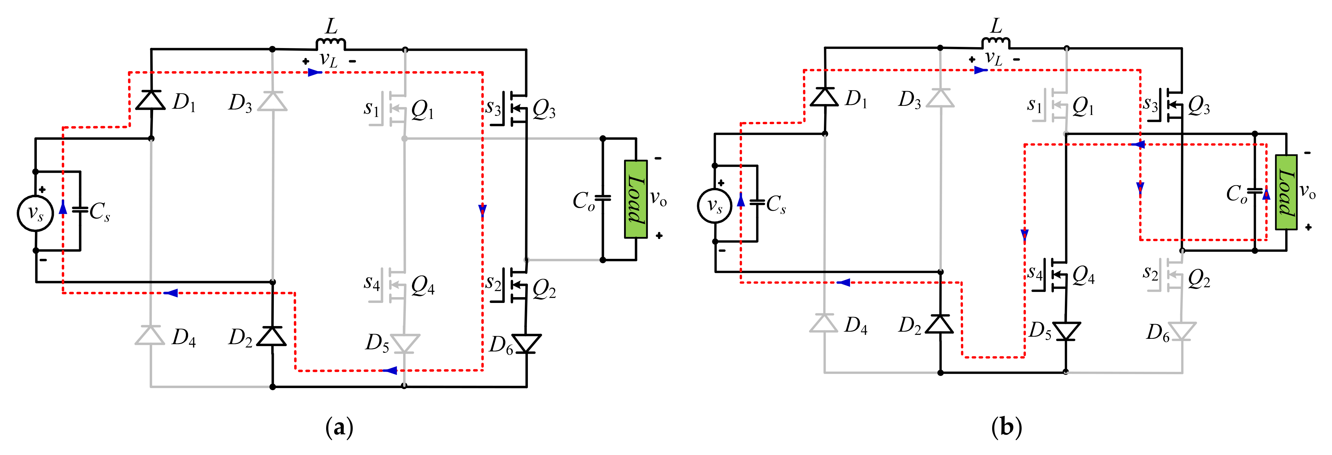
2.2. Voltage Control with Inverting Characteristics
The role of the front-end diode bridge remains similar as discussed for the non-inverting operation. It is an absolute value converter that transforms the sinusoidal input voltage to its absolute form. The peak voltage across the reverse-biasing diodes of this bridge cannot exceed the peak value of the input voltage. Thus, the diode bridge always delivers a time-varying unidirectional voltage at the input of the transistor’s bridge. This voltage is transformed to a regulated bidirectional voltage with boost characteristics. For the inverting operation, the control process for switching transistors
Q1 and
Q3 is inverted, as can be seen in
Figure 7b. The PWM behavior of switching transistor
Q4 for the non-inverting operation is changed to
Q2 for a positive input and vice versa for a negative input. This means that the PWM control of switching transistors
Q4 and
Q2 stabilizes the positive and negative output for non-inverting and inverting operations, respectively.
Figure 9a–d illustrate the transfer of power for a positive and negative regulated output voltage.
A similar approach as used for the non-inverting operation may be employed to compute the dynamic value of the inductor voltage and capacitor current during the PWM turn-on and -off period by using the KVL and KCL, respectively.
The dynamic values of the inductor current and capacitor voltage during the steady-state condition can be ignored due to the low variation in the required output frequency. Thus, the right-hand sides of Equations (11)–(14) are added, respectively, to obtain the voltage and current transfer ratio.
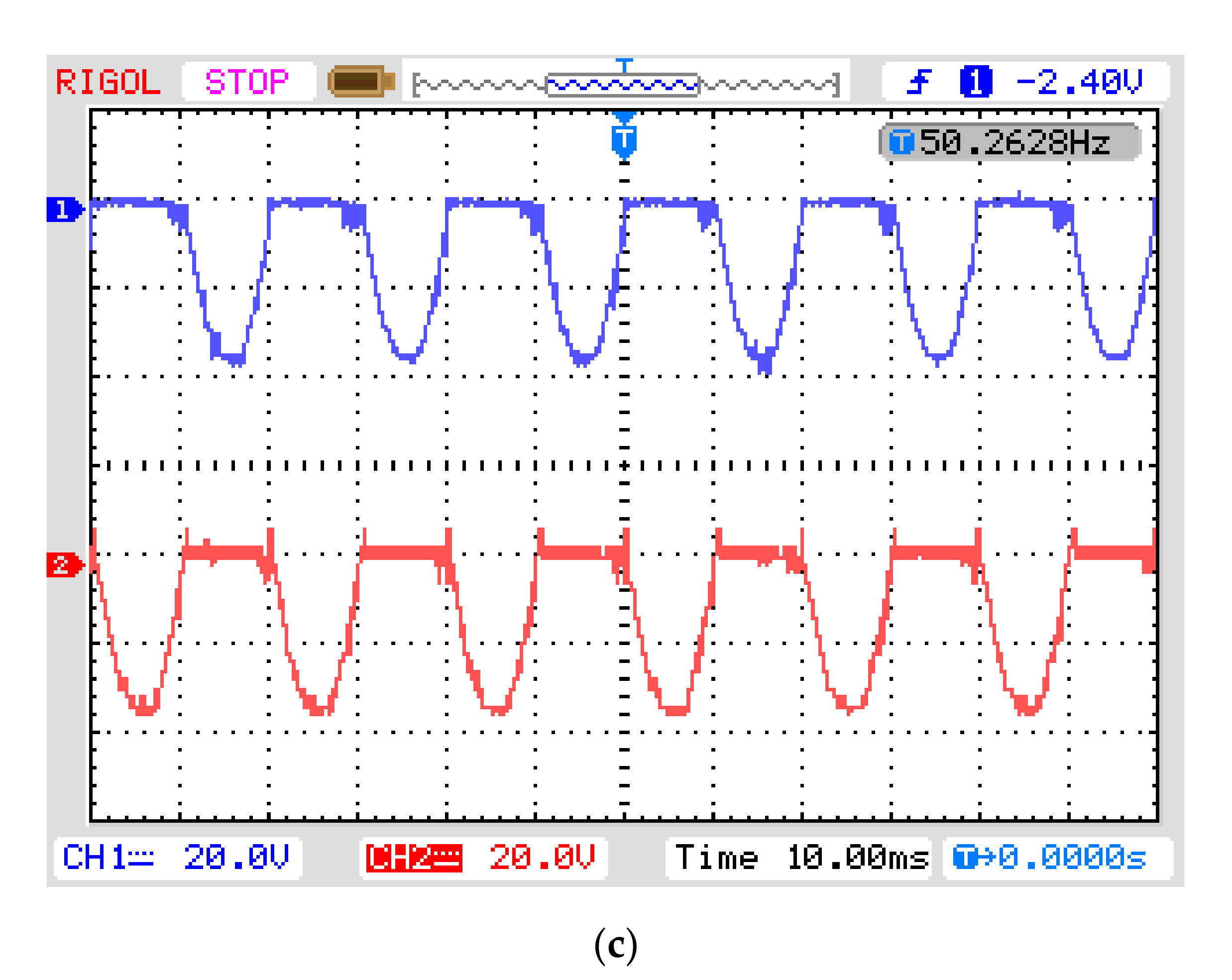
3. Comparative Analysis
The use of fewer (four) switching transistors and diodes (six) decreases the volume and cost of the converter. The control signal generated by any digital controller (microcontroller or processor) is not able to directly govern the switching states (on-to-off and off-to-on) of a switching transistor as their voltage level is as low (normally 0 to 5V) as that of the power circuit. Thus, electrical isolation of the high-voltage side to a low voltage level is mandatory. For this purpose, the turn-on and turn-off control of a switching transistor requires the use of one gate-controlling (driving) circuit and one isolated DC source. The realization of a gate-controlling circuit is achieved by employing a hybrid chip along with many passive components and microelectronic devices. In the same way, the implementation of an isolated DC source needs a low-frequency step-down transformer, a bridge rectifier, and filtering components to smooth the output. Therefore, the size and cost of the gate-controlling circuit and isolated DC source are much larger than those of a switching transistor. The total volume and cost of the converter heavily depend on the number of switching transistors. In addition, the proposed topology requires fewer diodes as well. Thus, the elimination of diodes and switching transistors is the major achievement of the proposed circuit topology. A bipolar voltage gain boost converter, as reported in [
20], is realized with the use of six switching transistors (six gate-controlling circuits and six isolated DC sources) and eight diodes. However, the developed circuit can be used to realize all outputs of [
20] with the help of four transistors (four controlling circuits and isolated DC sources) and six diodes only. Therefore, the realization of the proposed topology drastically reduces the overall volume and cost.
It can be seen for any of the conducting intervals in all operating modes of
Figure 8 and
Figure 9 that the operation of two switching transistors and three diodes realizes the required result. There is no change in the average conduction losses of the developed circuit and the circuit in [
20]. Equation (17) illustrates the average conduction losses caused by one switching transistor and one diode. Here, ‘
Vd’, ‘
Rd’ and ‘
Rm’ represent the forward voltage of the diode, forward resistance of the diode, and on-state resistance of the switching transistor, respectively.
In one cycle operation of the output voltage, four transistors and six diodes are to be conducted to realize the output. The total average conduction losses may be expressed as
By employing the approach as used in [
20], the average switching losses of a transistor and diode are calculated with the value of switching frequency (
fs) and reverse recovery charge (
QRR).
It can be observed that switching losses are directly related to the switching frequency, so the switching losses of the low-frequency-operated diodes are negligible. In the proposed topology and the circuit in [
20], there are only four conduction diodes (two for each half-cycle) at the high switching frequency. The total average switching losses can be computed as
In summary, the validation of the proposed converter is carried out by comparing its performance indexed with the existing converter realized with a similar approach, as can be seen in
Table 1.
The comparative analysis of the suggested circuit with the circuit reported in [
20] illustrates that the use of a smaller number of solid-state devices increases its potential to be applied as an AC voltage controller with a voltage having non-inverting and inverting capabilities.


 ,
, 


