
Maple-Leaf Shaped Broadband Optical Nano-Antenna with Hybrid Plasmonic Feed for Nano-Photonic Applications


 ,
, 
 , ,
, ,  and
and 
Abstract
:1. Introduction
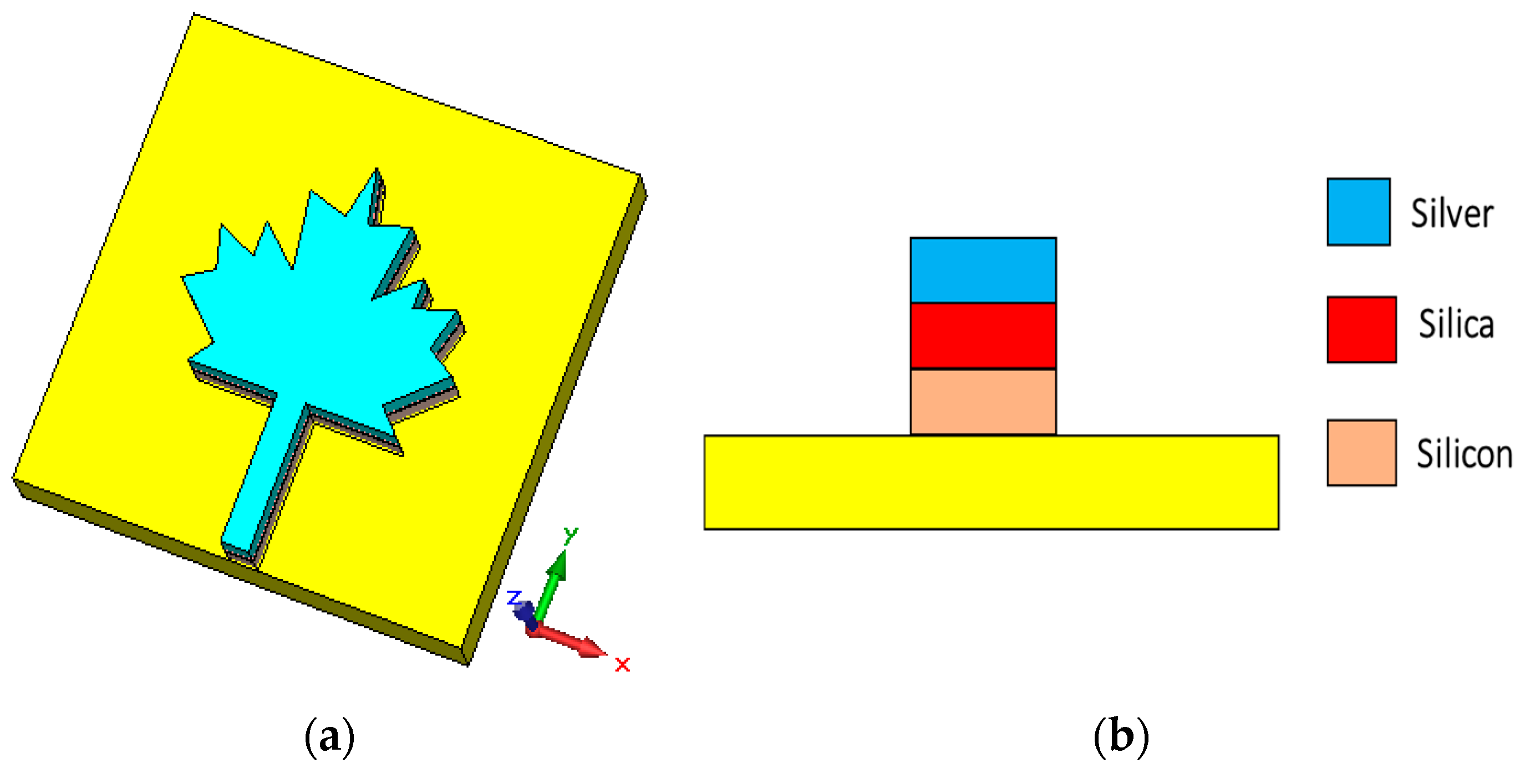
2. Structure
2.1. Modeling and Characterization of Hybrid Plasmonic Waveguide
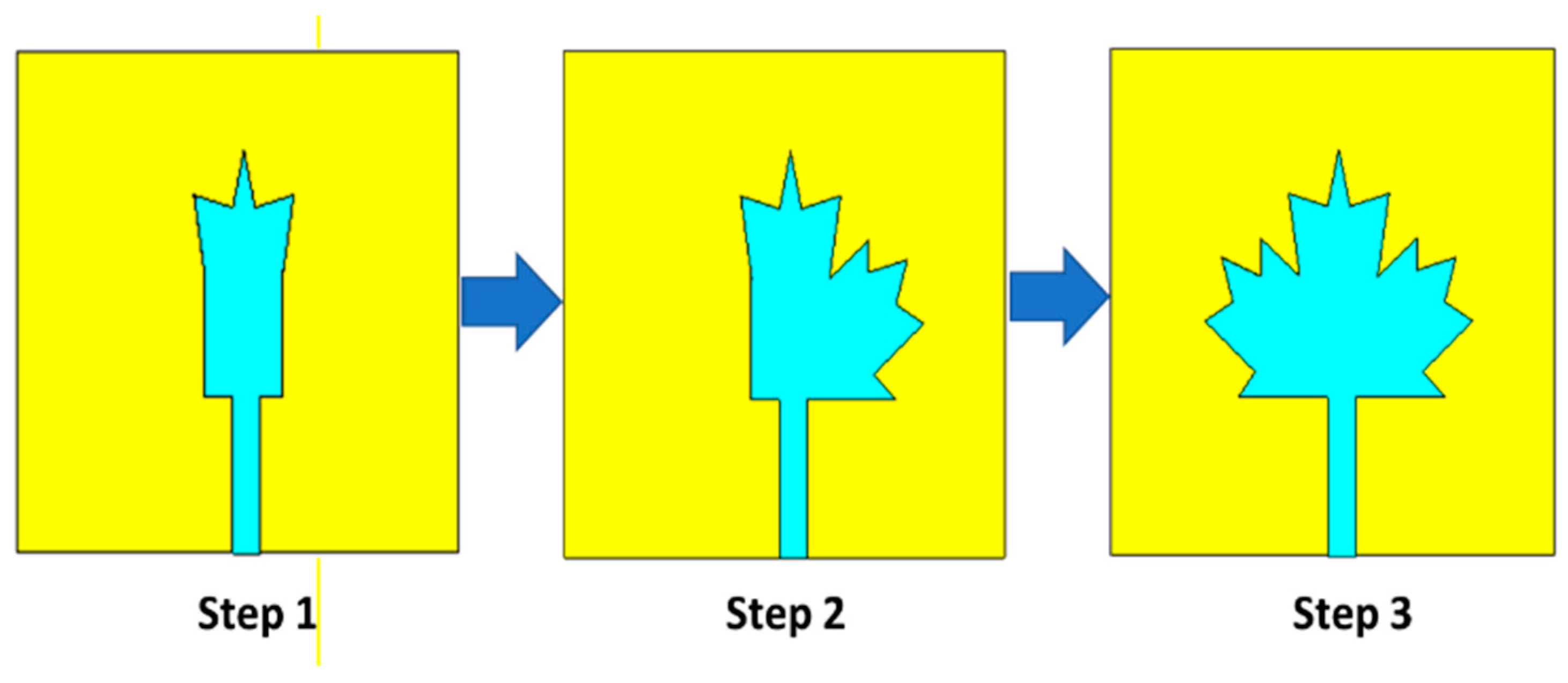
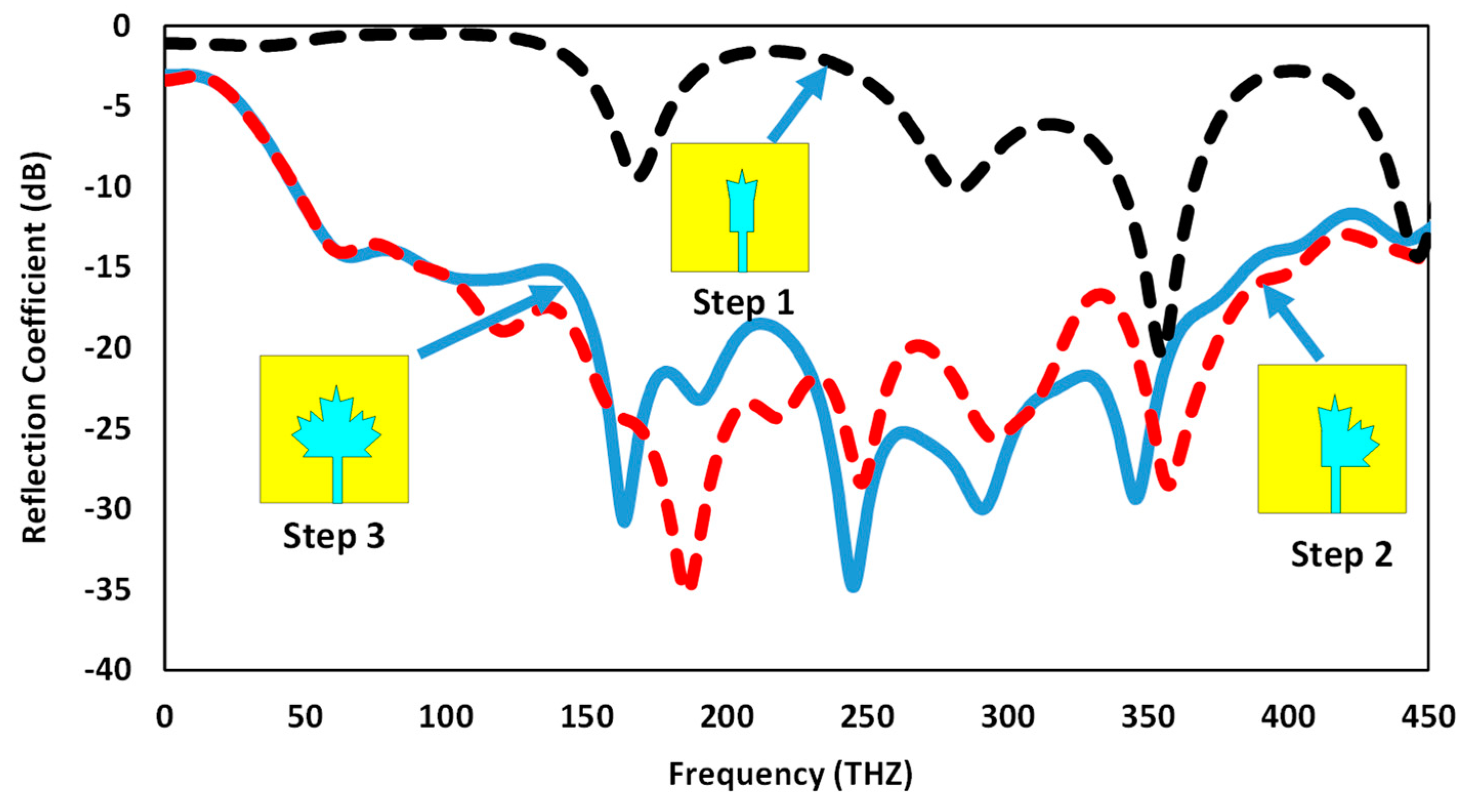
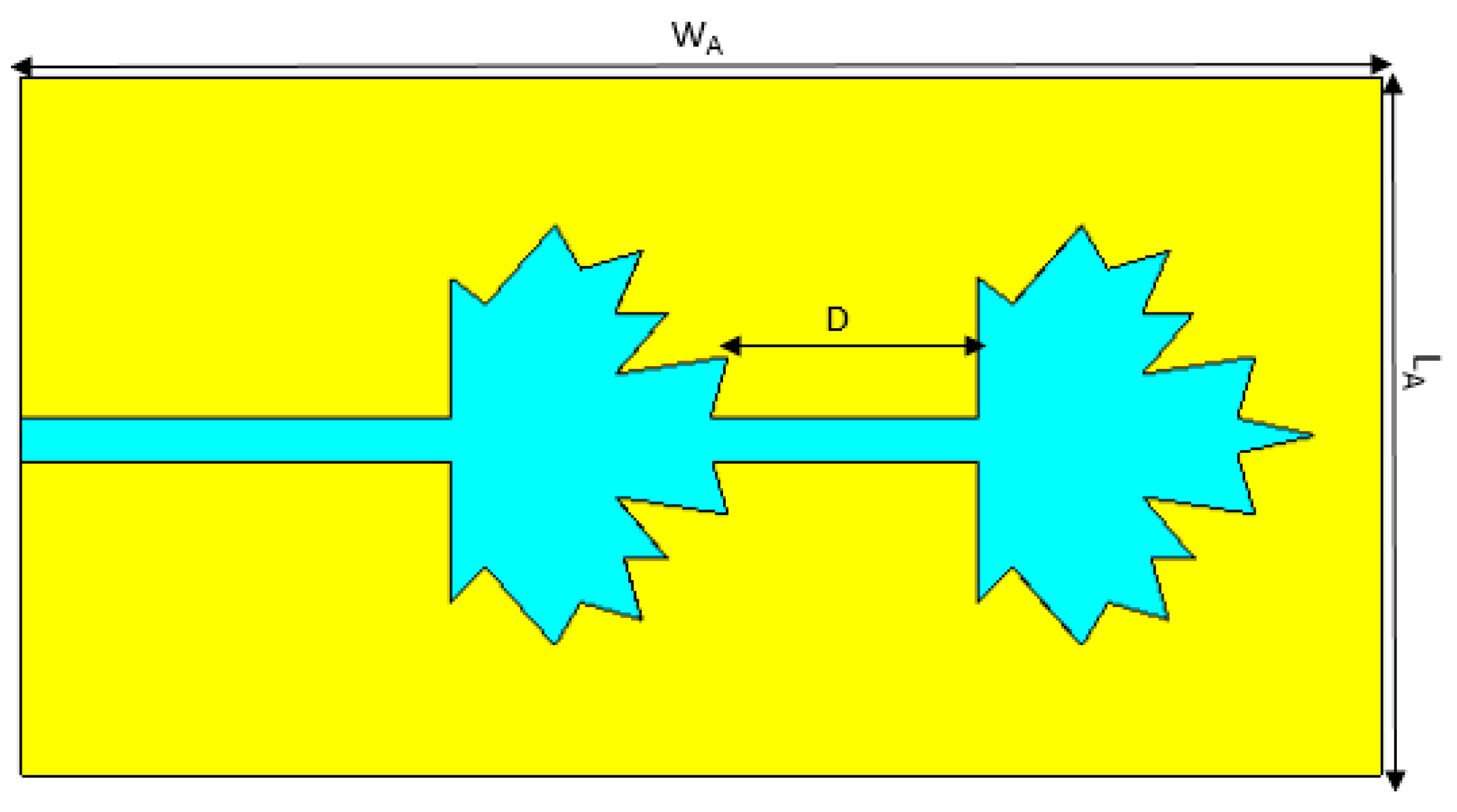
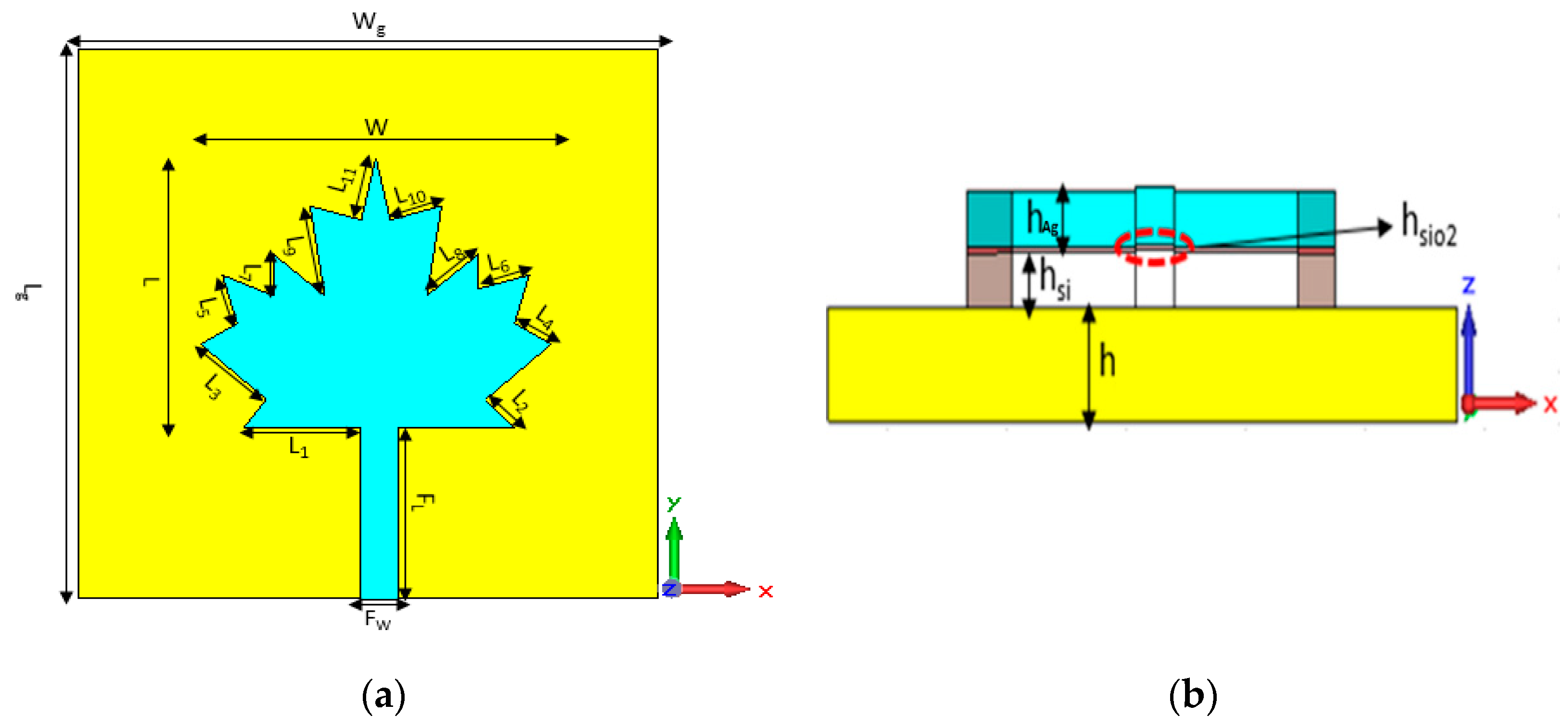
2.2. Design of the Nano-Antenna
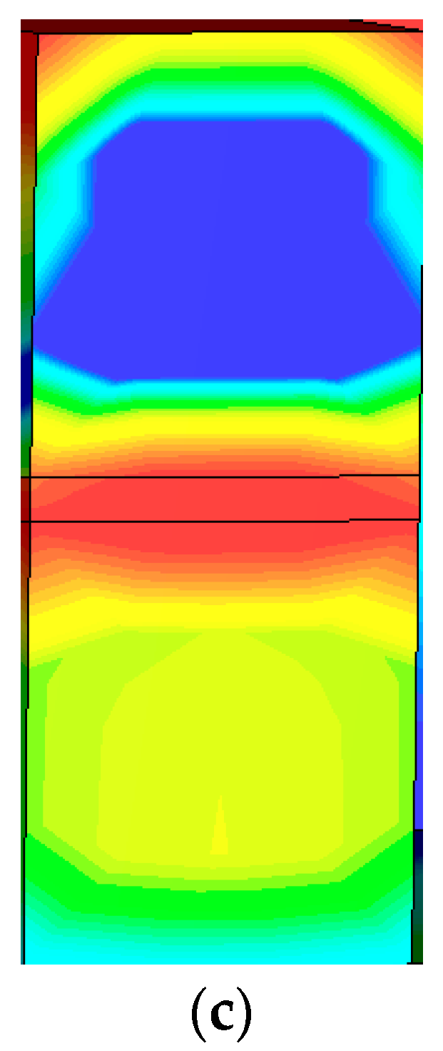
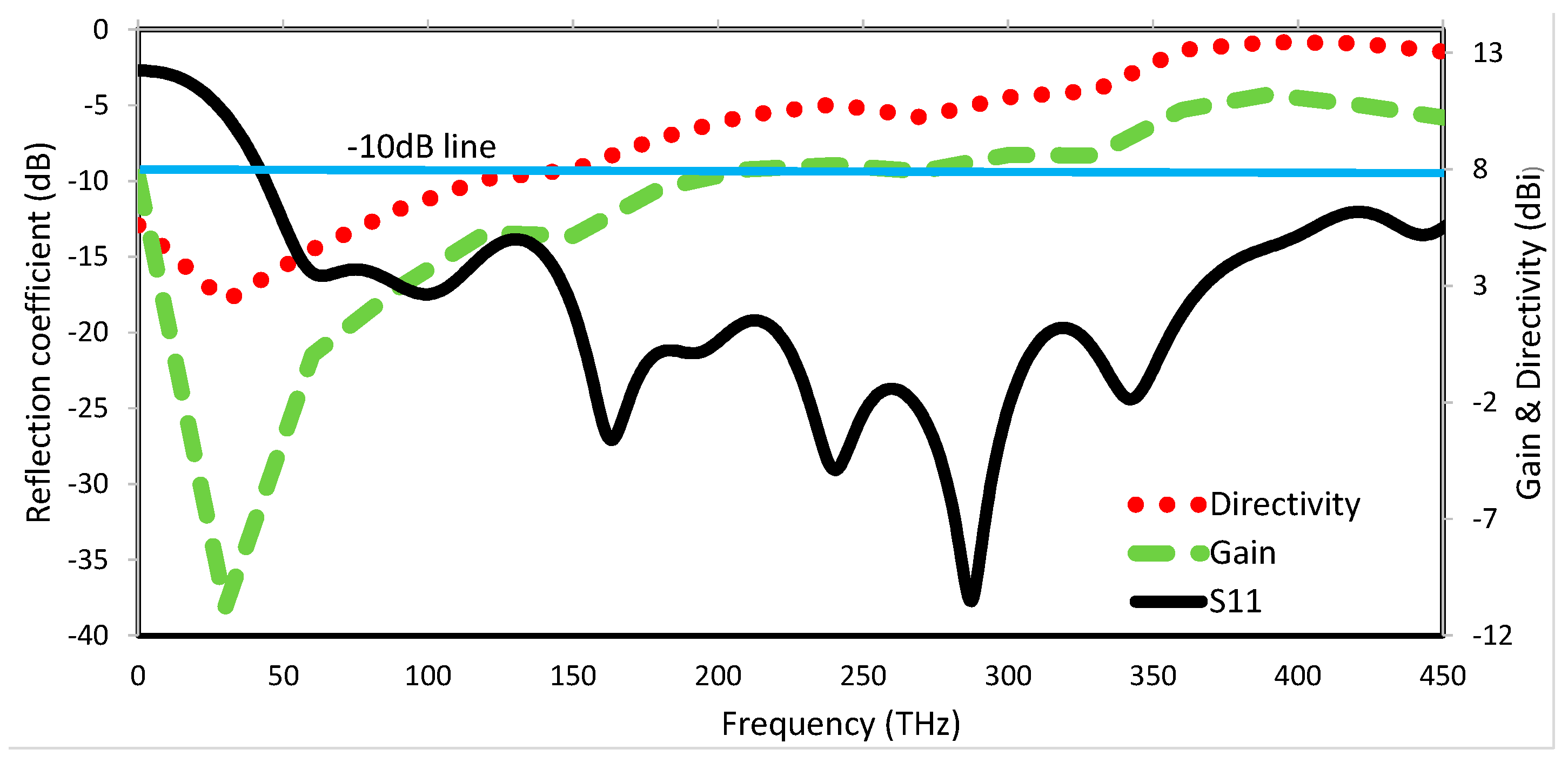
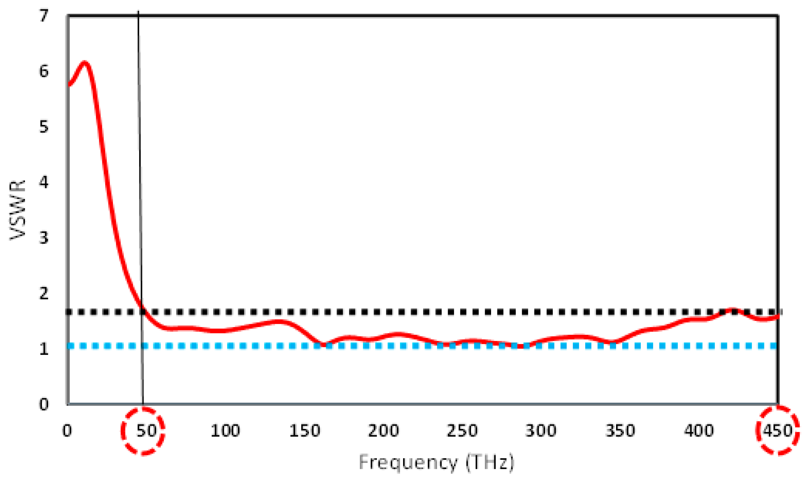
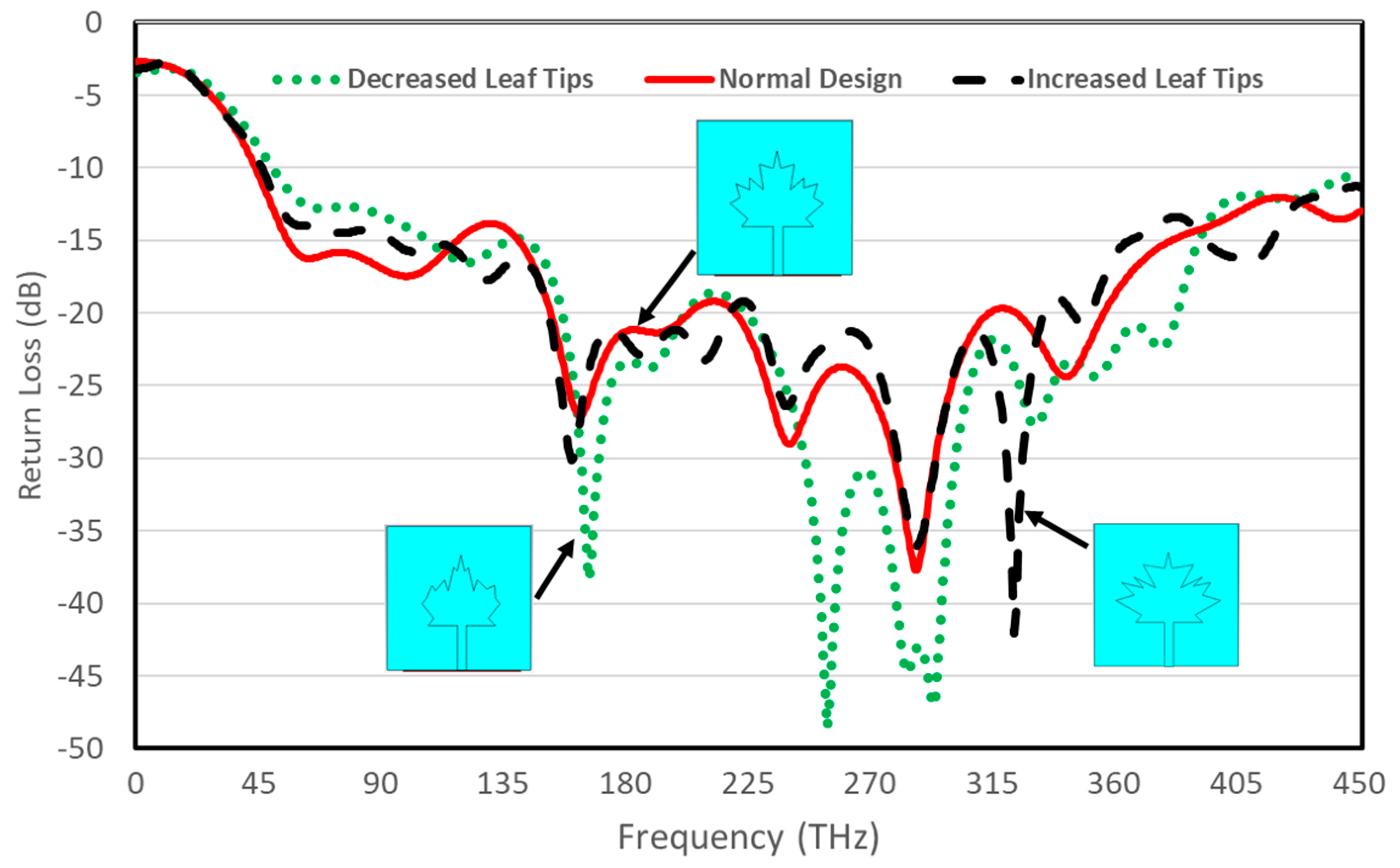
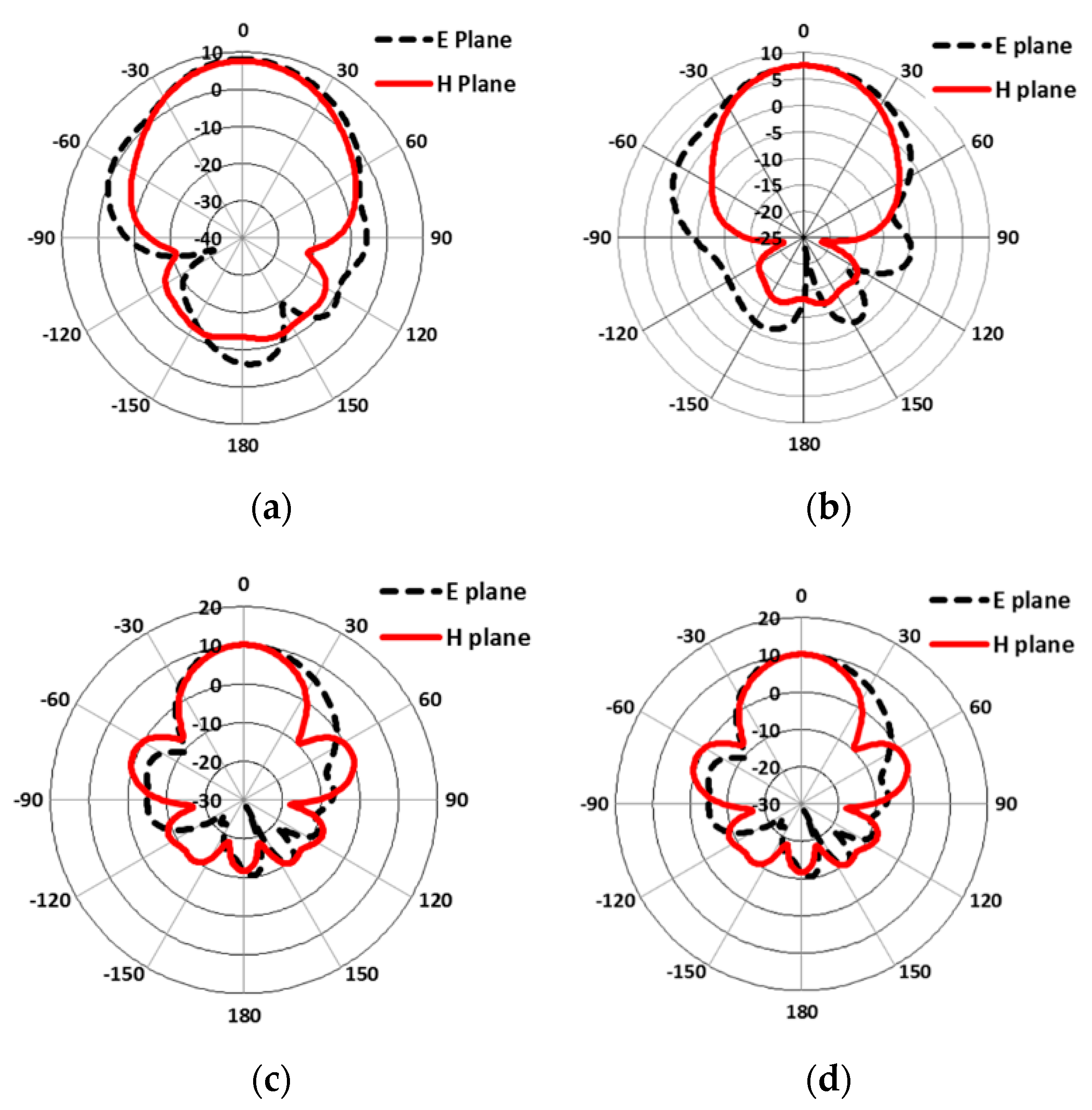
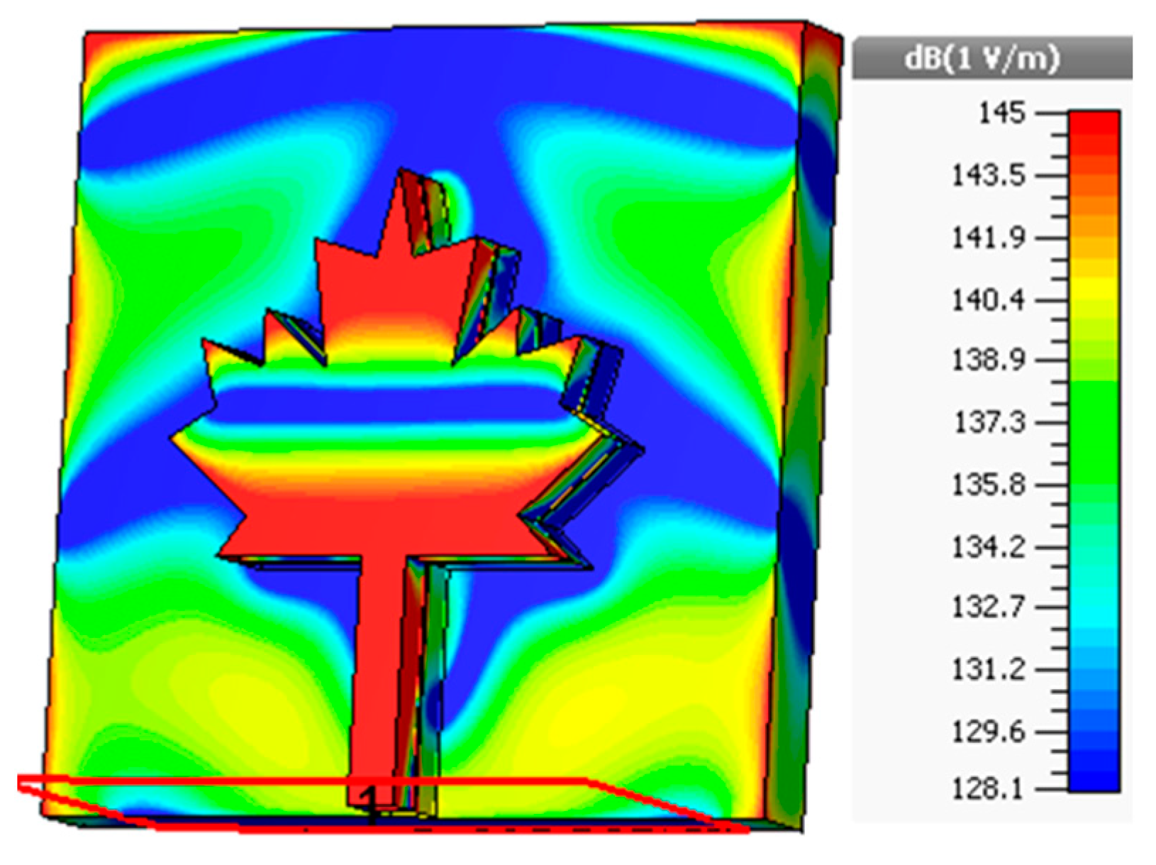
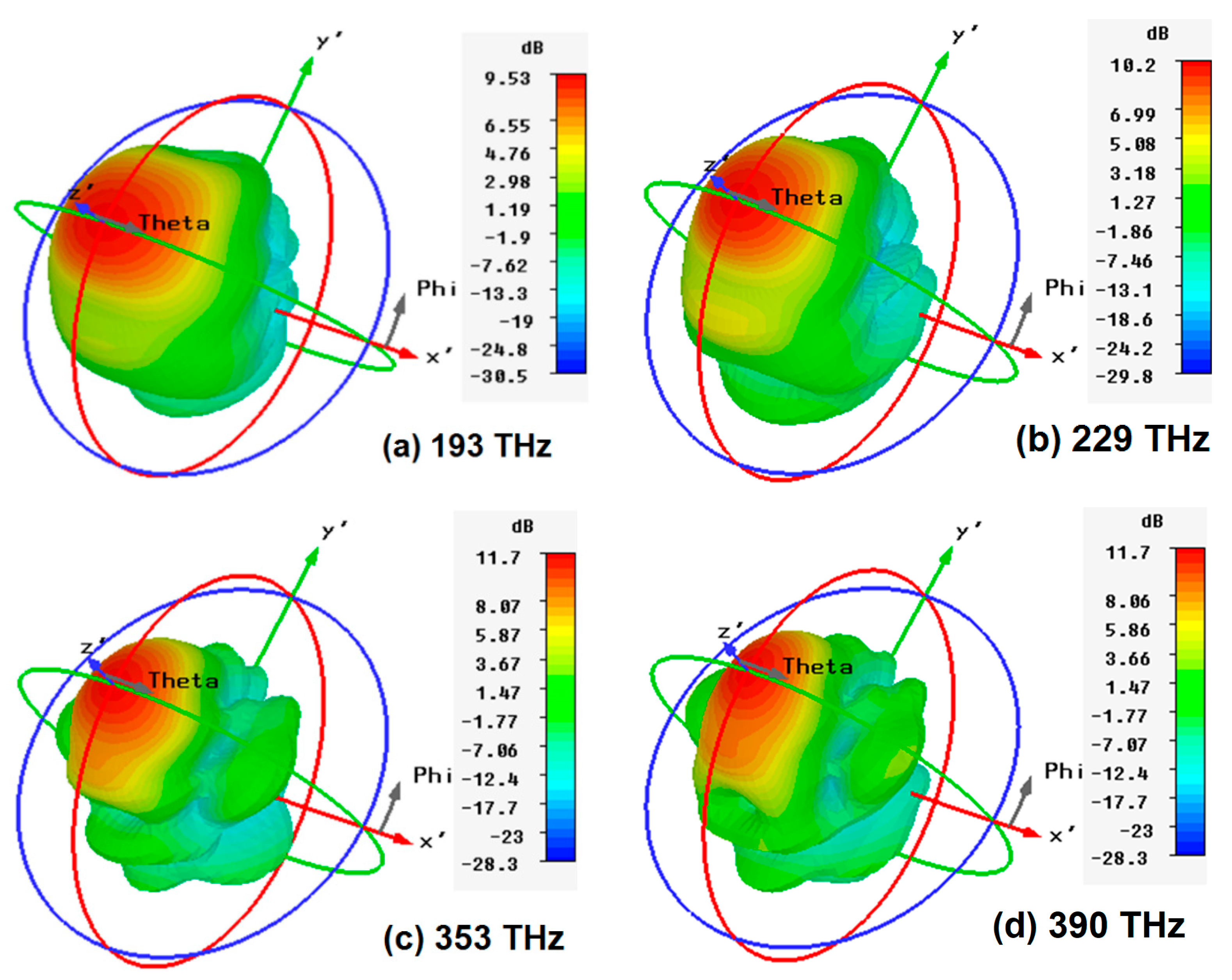
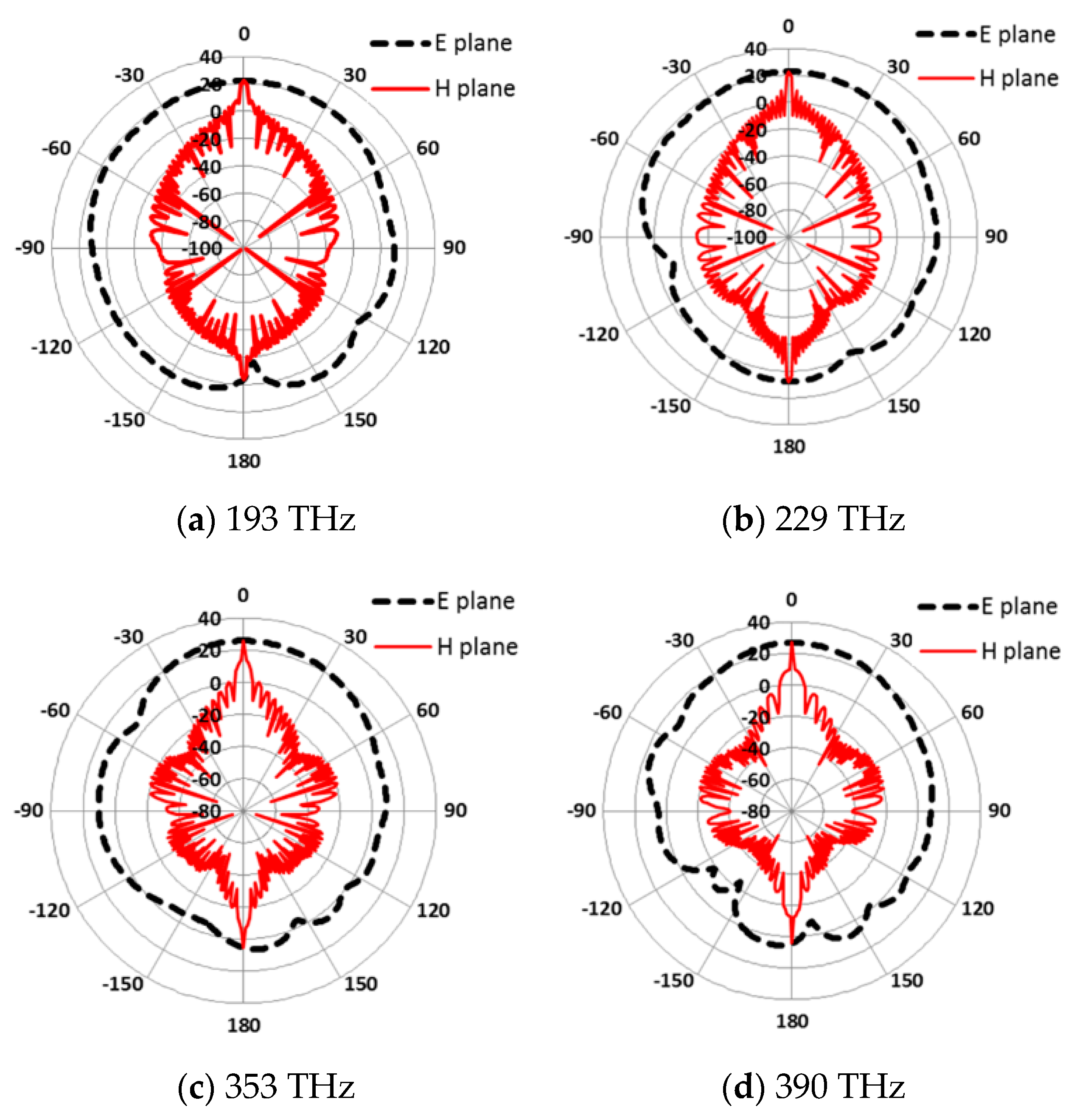
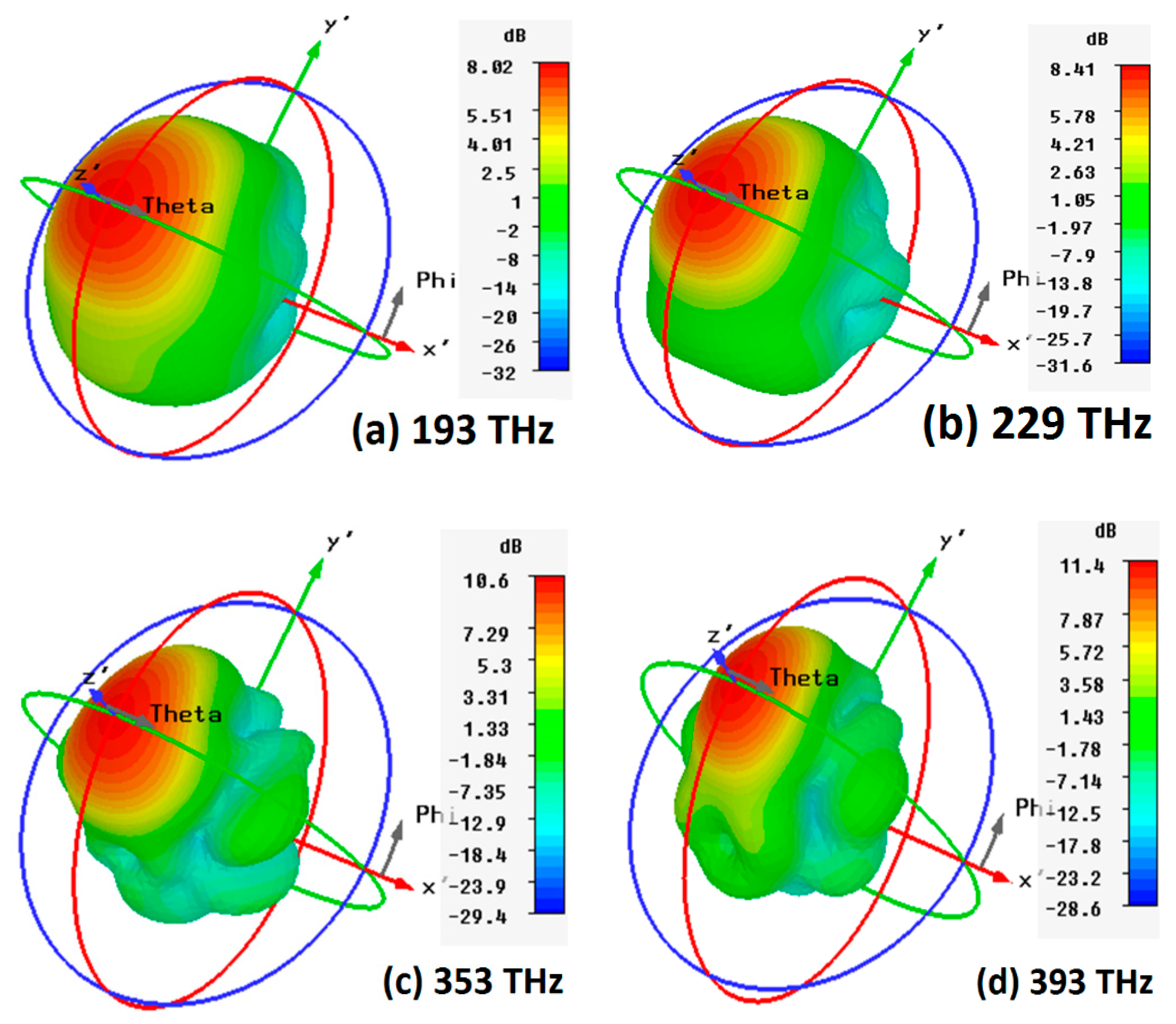
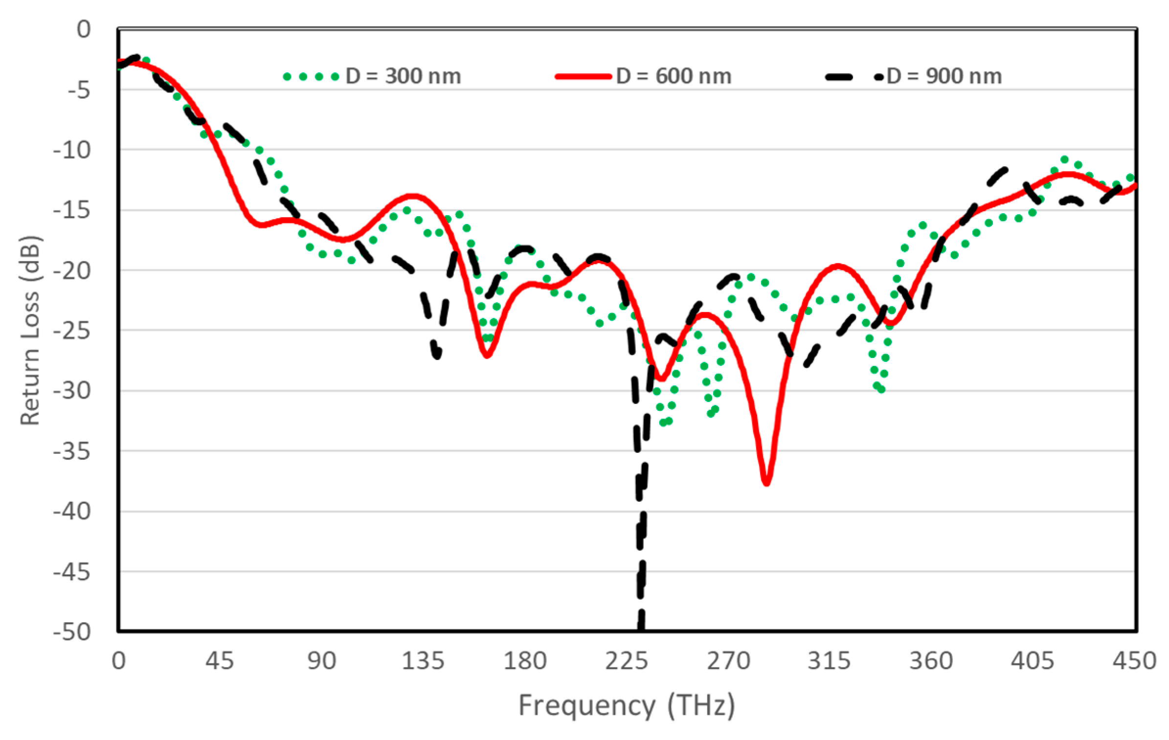
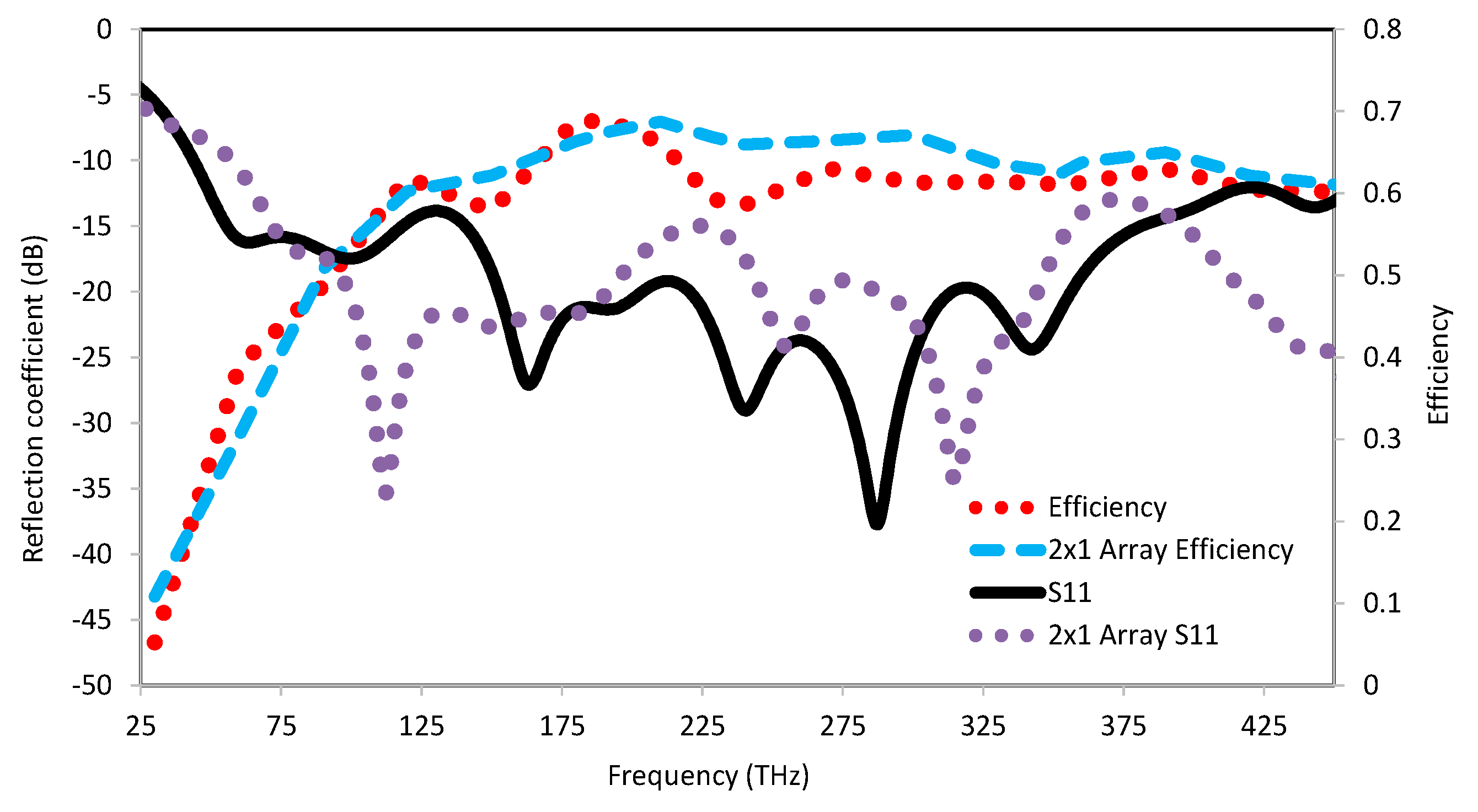
3. Simulation and Results
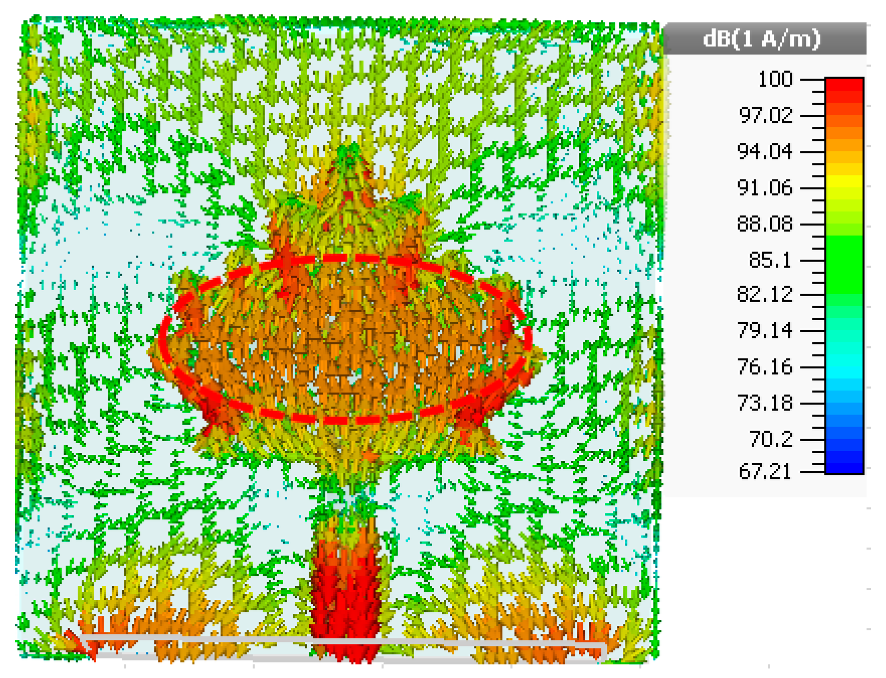
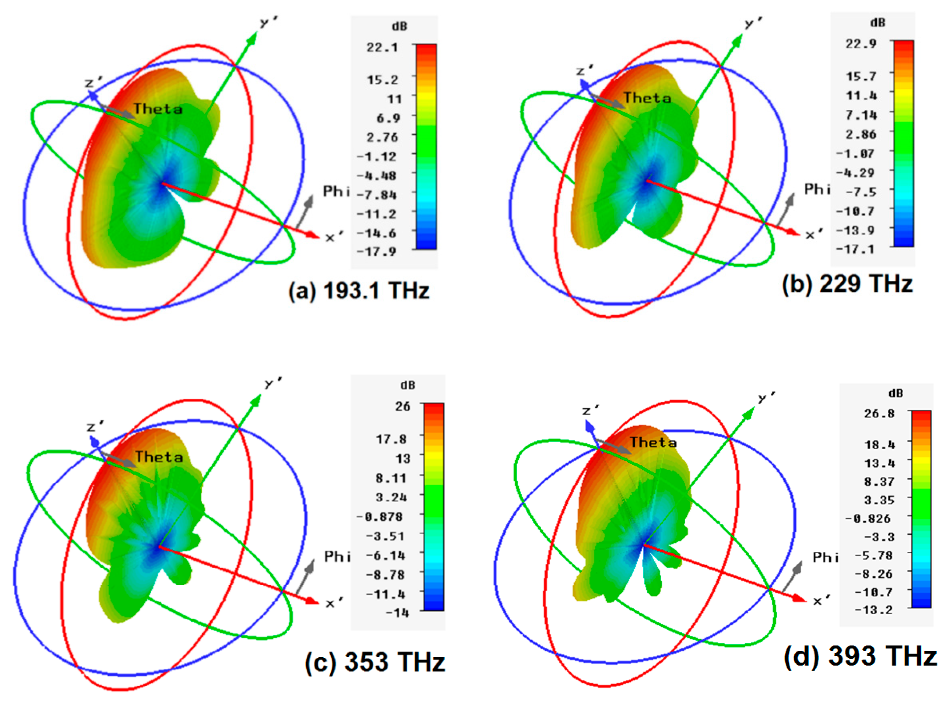
4. Antenna Array for Energy Harvesting Applications
5. Conclusions
Author Contributions
Funding
Institutional Review Board Statement
Informed Consent Statement
Data Availability Statement
Acknowledgments
Conflicts of Interest
References
- Ullah, S.; Ahmad, I.; Raheem, Y.; Ullah, S.; Ahmad, T.; Habib, U. Hexagonal shaped CPW feed based frequency reconfigurable antenna for WLAN and sub-6 GHz 5G applications. In Proceedings of the IEEE 2020 International Conference on Emerging Trends in Smart Technologies (ICETST), Karachi, Pakistan, 26–27 March 2020; pp. 1–4. [Google Scholar]
- Panda, R.A.; Kumari, P.; Naik, J.; Negi, P.; Mishra, D. Flower Shaped Patch with Circular Defective Ground Structure for 15 GHz Application. In International Conference on Innovations in Bio-Inspired Computing and Applications; Springer: Cham, Switzerland, 2019; pp. 243–249. [Google Scholar]
- Abolade, J.O.; Konditi, D.B.O.; Dharmadhikary, V.M. Bio-inspired wideband antenna for wireless applications based on perturbation technique. Heliyon 2020, 6, e04282. [Google Scholar] [CrossRef]
- De Oliveira, M.A.; da Costa, A.P.; Forte, G.G.S.; de Melo, P.-K.P.; Fontgalland, G.; Silva, P.-H.F.; Fontgalland, I.L. Using polar transformation to design a dissimilar antenna array inspired on four-leaf clover. In Proceedings of the 2018 IEEE Radio and Wireless Symposium (RWS), Anaheim, CA, USA, 15–18 January 2018; pp. 228–230. [Google Scholar]
- Abolade, J.O.; Konditi, D.B.; Dharmadhikary, V.M. Compact Vitis vinifera-Inspired Ultrawideband Antenna for High-Speed Communications. Int. J. Antennas Propag. 2021, 2021, 9975884. [Google Scholar] [CrossRef]
- da Silva Júnior, P.F.; Carlos, R.; Freire, S.; René Serres, A.J.; da Fonseca Silva, P.H.; Costa Silva, J. Bio-Inspired Antenna for UWB Systems. In Proceedings of the 2016 1st International Symposium on Instrumentation Systems, Circuits and Transducers (INSCIT), Belo Horizonte, Brazil, 29 August 2016–3 September 2016; p. 16408466. [Google Scholar]
- Mesquita, M.D.S.; D’Assunção, A.G.; Oliveira, J.B.L.; Batista, Y.M.V. A New Conductive Ink for Microstrip Antenna and Bioinspired FSS Designs on Glass and Fiberglass Substrates. J. Microw. Optoelectron. Electromagn. Appl. 2019, 18, 227–245. [Google Scholar] [CrossRef]
- Malik, R.; Singh, P.; Ali, H.; Goel, T. A Star Shaped Superwide Band Fractal Antenna for 5G Applications. In Proceedings of the 2018 3rd International Conference for Convergence in Technology (I2CT), Pune, India, 6–8 April 2018; pp. 1–6. [Google Scholar]
- Anguera, J.; Puente, C.; Borja, C.; Soler, J. Fractal-Shaped Antennas: A Review. In Wiley Encyclopedia of RF and MicrowaveEngineering; Chang, K., Ed.; JohnWiley & Sons, Inc.: New York, NY, USA, 2005; Volume 2, pp. 1620–1635. [Google Scholar]
- Melchiorre, L.; Marasco, I.; Niro, G.; Basile, V.; Marrocco, V.; D’Orazio, A.; Grande, M. Bio-Inspired Dielectric Resonator Antenna for Wideband Sub-6 GHz Range. Appl. Sci. 2020, 10, 8826. [Google Scholar] [CrossRef]
- Marrocco, V.; Basile, V.; Marasco, I.; Niro, G.; Melchiorre, L.; D’Orazio, A.; Grande, M.; Fassi, I. Rapid Prototyping of Bio-Inspired Dielectric Resonator Antennas for Sub-6 GHz Applications. Micromachines 2021, 12, 1046. [Google Scholar] [CrossRef]
- Bharadwaj, P.; Deutsch, B.; Novotny, L. Optical antennas. Adv. Opt. Photonics 2009, 1, 438–483. [Google Scholar] [CrossRef] [Green Version]
- Duman, H. Design and Fabrication of Resonant Nanoantennas on Chalcogenide Glasses for Nonlinear Photonic Applications; Bilkent University: Ankara, Turkey, 2013. [Google Scholar]
- Yuming, W. Analysis and Design of Nanoantennas. Ph.D. Dissertation, National University of Singapore, Singapore, 2010. [Google Scholar]
- Haroyan, H.S.; Tadevosyan, V.R. High Gain Broadband Plasmonic Slot Nano-Antenna. Int. J. Phys. Math. Sci. 2015, 9, 1104–1107. [Google Scholar]
- Sethi, W.T.; Vettikalladi, H.; Fathallah, H.; Himdi, M. Hexagonal dielectric loaded nantenna for optical ITU-T C-band communication. In Proceedings of the 2015 IEEE 11th International Conference on Wireless and Mobile Computing, Networking and Communications (WiMob), Abu Dhabi, United Arab Emirates, 19–21 October 2015; pp. 604–607. [Google Scholar]
- Zhou, R.; Ding, J.; Arigong, B.; Lin, Y.; Zhang, H. Design of a new broadband monopole optical nano-antenna. J. Appl. Phys. 2013, 114, 184305. [Google Scholar] [CrossRef]
- Kausar, A.S.M.Z.; Reza, A.W.; Latef, T.A.; Ullah, M.H.; Karim, M.E. Optical nano antennas: State of the art, scope and challenges as a biosensor along with human exposure to nano-toxicology. Sensors 2015, 15, 8787–8831. [Google Scholar] [CrossRef] [Green Version]
- Rosner, B.; Peck, J.; van der Weide, D. Near-field antennas integrated with scanning probes for THz to visible microscopy: Scale modeling and limitations on performance. IEEE Trans. Antennas Propag. 2002, 50, 670–675. [Google Scholar] [CrossRef]
- Xu, T.; Wu, Y.-K.; Luo, X.; Guo, L.J. Plasmonic nanoresonators for high-resolution colour filtering and spectral imaging. Nat. Commun. 2010, 1, 59. [Google Scholar] [CrossRef] [PubMed]
- Tang, L.; Kocabas, S.E.; Latif, S.; Okyay, A.K.; Ly-Gagnon, D.S.; Saraswat, K.C.; Miller, D.A. Nanometre-scale germanium photodetector enhanced by a near-infrared dipole antenna. Nat. Photonics 2008, 2, 226–229. [Google Scholar] [CrossRef]
- Rabienejhad, M.J.; Mazaheri, A.; Davoudi-Darareh, M. Design and optimization of nano-antenna for thermal ablation of liver cancer cells. Chin. Phys. B 2021, 30, 048401. [Google Scholar] [CrossRef]
- Habib, U.; Aighobahi, A.; Wang, C.; Gomes, N.J. Radio over fiber transport of mm-Wave 2 × 2 MIMO for spatial diversity and multiplexing. In Proceedings of the IEEE International Topical Meeting on Microwave Photonics (MWP), Long Beach, CA, USA, 31 October 2016–3 November 2016; pp. 39–42. [Google Scholar]
- Tapio, K.; Mostafa, A.; Kanehira, Y.; Suma, A.; Dutta, A.; Bald, I. A Versatile DNA Origami-Based Plasmonic Nanoantenna for Label-Free Single-Molecule Surface-Enhanced Raman Spectroscopy. ACS Nano 2021, 15, 7065–7077. [Google Scholar] [CrossRef] [PubMed]
- Liu, Y.; Li, K.; Cao, S.; Xiong, G.; Zhu, L. Optimization Design of a Multi-slot Nanoantenna Based on Genetic Algorithm for Energy Harvesting. Plasmonics 2019, 14, 1577–1586. [Google Scholar] [CrossRef]
- Mora-Ventura, B.; Sánchez, J.E.; González, G.; González, F.J. Thermal impedance analysis of nano-dipole linear arrays for energy harvesting applications. Infrared Phys. Technol. 2020, 107, 103332. [Google Scholar] [CrossRef]
- Wu, Y.-M.; Li, L.-W.; Liu, B. Gold bow-tie shaped aperture Nanoantenna: Wide band near-field resonance and far-field radiation. IEEE Trans. Magn. 2010, 46, 1918–1921. [Google Scholar] [CrossRef]
- Miroshnichenko, A.E.; Maksymov, I.S.; Davoyan, A.R.; Simovski, C.; Belov, P.; Kivshar, Y.S. An arrayed nanoantenna for broadband light emission and detection. Phys. Status Solidi (RRL)-Rapid Res. Lett. 2011, 5, 347–349. [Google Scholar] [CrossRef] [Green Version]
- Biagioni, P.; Huang, J.S.; Duò, L.; Finazzi, M.; Hecht, B. Cross Resonant Optical Antenna. Phys. Rev. Lett. 2009, 102, 256801. [Google Scholar] [CrossRef] [PubMed] [Green Version]
- Ahmad, I.; Ullah, S.; Ullah, S.; Habib, U.; Ahmad, S.; Ghaffar, A.; Alibakhshikenari, M.; Khan, S.; Limiti, E. Design and Analysis of a Photonic Crystal Based Planar Antenna for THz Applications. Electronics 2021, 10, 1941. [Google Scholar] [CrossRef]
- Zainud-Deen, S.H.; Malhat, H.A.; El-Refaay, E.A. Polarization-Independent Reconfigurable Graphene Gas Sensor Using Crescent Plasmonic Antenna. Plasmonics 2020, 15, 1115–1122. [Google Scholar] [CrossRef]
- Dong, Z.; Sun, C.; Si, J.; Deng, X. A tunable plasmonic nano-antenna based on metal–graphene double-nanorods. Laser Phys. Lett. 2018, 15, 056202. [Google Scholar] [CrossRef]
- Yong, Z.; Gong, C.; Dong, Y.; Zhang, S.; He, S. Broadband localized electric field enhancement produced by a single-element plasmonic nanoantenna. RSC Adv. 2017, 7, 2074–2080. [Google Scholar] [CrossRef] [Green Version]
- Iluz, Z.; Boag, A. Wideband dual Vivaldi nano-antenna with high radiation efficiency over the infrared frequency band. In Proceedings of the 2011 IEEE International Conference on Microwaves, Communications, Antennas and Electronics Systems (COMCAS), Tel Aviv, Israel, 5 July 2011; pp. 1–3. [Google Scholar]
- Gramotnev, D.K.; Bozhevolnyi, S.I. Plasmonics beyond the diffraction limit. Nat. Photonics 2010, 4, 83–91. [Google Scholar] [CrossRef]
- Economou, E.N. Surface plasmons in thin films. Phys. Rev. 1969, 182, 539. [Google Scholar] [CrossRef]
- Maier, S.A.; Kik, P.G.; Atwater, H.A.; Meltzer, S.; Harel, E.; Koel, B.E.; Requicha, A.A.G. Local detection of electromagnetic energy transport below the diffraction limit in metal nanoparticle plasmon waveguides. Nat. Mater. 2003, 2, 229–232. [Google Scholar] [CrossRef]
- Vernon, K.C.; Gramotnev, D.K.; Pile, D.F. Adiabatic nanofocusing of plasmons by a sharp metal wedge on a dielectric substrate. J. Appl. Phys. 2007, 101, 104312. [Google Scholar] [CrossRef] [Green Version]
- Gielis, J. A generic geometric transformation that unifies a wide range of natural and abstract shapes. Am. J. Bot. 2003, 90, 333–338. [Google Scholar] [CrossRef] [PubMed]
- Yousefi, L. Highly directive hybrid plasmonic leaky wave optical nano-antenna. Prog. Electromagn. Res. Lett. 2014, 50, 85–90. [Google Scholar] [CrossRef] [Green Version]
- Alam, M.Z. Hybrid Plasmonic Waveguides: Theory and Applications; University of Toronto: Toronto, ON, Canada, 2012. [Google Scholar]
- Ctyrokỳ, J.; Kwiecien, P.; Richter, I. Analysis of hybrid dielectric-plasmonic slot waveguide structures with 3D Fourier Modal Methods. J. Eur. Opt. Soc.-Rapid Publ. 2013, 8, 13024. [Google Scholar] [CrossRef] [Green Version]
- Yang, Y.; Li, Q.; Qiu, M. Broadband nanophotonic wireless links and networks using on-chip integrated plasmonic antennas. Sci. Rep. 2016, 6, 19490. [Google Scholar] [CrossRef] [Green Version]
- Yousefi, L.; Foster, A.C. Waveguide-fed optical hybrid plasmonic patch nano-antenna. Opt. Express 2012, 20, 18326–18335. [Google Scholar] [CrossRef] [PubMed] [Green Version]
- CST Microwave Studio CST of America, Inc. Available online: http://www.cst.com (accessed on 17 September 2021).
- Haque, A.; Reza, A.W.; Kumar, N.; Ramiah, H. Slotting effect in designing circular edge bow-tie nano antenna for energy harvesting. In Proceedings of the 2015 IEEE Conference on Open Systems (ICOS), Melaka, Malaysia, 24–26 August 2015; pp. 46–50. [Google Scholar]
- Saad-Bin-Alam, M.; Khalil, M.I.; Rahman, A.; Chowdhury, A.M. Hybrid Plasmonic Waveguide Fed Broadband Nanoantenna for Nano photonic Applications. IEEE Photonics Technol. Lett. 2015, 27, 1092–1095. [Google Scholar] [CrossRef] [Green Version]
- Bozzetti, M.; de Candia, G.; Gallo, M.; Losito, O.; Mescia, L.; Prudenzano, F. Analysis and design of a solar rectenna. In Proceedings of the IEEE International Symposium on Industrial Electronics (ISIE 2010), Bari, Italy, 4–7 July 2010; pp. 2001–2004. [Google Scholar]
- Nourmohammadi, A.; Nikoufard, M. Ultra-Wideband Photonic Hybrid Plasmonic Horn Nanoantenna with SOI Configuration. Silicon 2020, 12, 193–198. [Google Scholar] [CrossRef]
- Sharma, P.; Vishwakarma, D.K. Long Range Multilayer Hybrid Plasmonic Waveguide Components and Integrated Circuit. IEEE Trans. Nanotechnol. 2019, 18, 940–947. [Google Scholar] [CrossRef]
- Malheiros-Silveira, G.N.; Wiederhecker, G.S.; Hernández-Figueroa, H.E. Dielectric resonator antenna for applications in nanophotonics. Opt. Express 2013, 21, 1234–1239. [Google Scholar] [CrossRef]
- Nikoufard, M.; Nourmohammadi, A.; Esmaeili, S. Hybrid Plasmonic Nanoantenna with the Capability of Monolithic Integration with Laser and Photodetector on InP Substrate. IEEE Trans. Antennas Propag. 2018, 66, 3–8. [Google Scholar] [CrossRef]
- Balanis, C.A. Antenna Theory: Analysis and Design, 4th ed.; John Wiley & Sons: New York, NY, USA, 2016. [Google Scholar]


| Parameters | Values (nm) | Parameters | Values (nm) |
|---|---|---|---|
| W | 960 | L6 | 155 |
| L | 780 | L7 | 125 |
| Wg | 1600 | L8 | 200 |
| Lg | 1600 | L9 | 280 |
| FL | 500 | L10 | 155 |
| FW | 100 | L11 | 200 |
| L1 | 380 | hAg | 100 |
| L2 | 115 | his | 100 |
| L3 | 250 | hSiO2 | 10 |
| L4 | 125 | Hg | 200 |
| L5 | 155 | D | 600 |
| WA | 1600 | LA | 3160 |
| References | [47] | [44] | [49] | [50] | [51] | [52] | This Work |
|---|---|---|---|---|---|---|---|
| Frequency (THz) | 193.5/229/352.9 | 193.5 | 193.5/229/352.9 | 193.5 | 193.5 | 193.5 | 193.5/229/352.9/393 |
| Gain (dBi) | 5.03/4.64/2.02 | 5.6 | 4.67/4.8/7.26 | 7.99 | 7.5 | 9 | 8.02/8.41/10.6/11.4 |
| Efficiency (%) | *** | 87 | *** | 84.56 | *** | 89 | 60 |
| Bandwidth (GHz) | 234 | 15.6 | 240 | 203 | 20 | 40 | 400 |
| Parameter | Gain (dBi) | ||
|---|---|---|---|
| Frequency (THz) | Single Element | 2 × 1 Array | 64 × 1 Array |
| 193 | 8.02/9.65 | 9.53/11.2 | 22.1/23.7 |
| 229 | 8.41/10.7 | 10.2/11.9 | 22.9/25.1 |
| 353 | 10.6/12.7 | 11.7/13.8 | 26/28.1 |
| 390 | 11.4/13.5 | 11.7/13.8 | 26.8/28.8 |
Publisher’s Note: MDPI stays neutral with regard to jurisdictional claims in published maps and institutional affiliations. |
© 2021 by the authors. Licensee MDPI, Basel, Switzerland. This article is an open access article distributed under the terms and conditions of the Creative Commons Attribution (CC BY) license (https://creativecommons.org/licenses/by/4.0/).
Share and Cite
Ahmad, I.; Ullah, S.; din, J.u.; Ullah, S.; Ullah, W.; Habib, U.; Khan, S.; Anguera, J. Maple-Leaf Shaped Broadband Optical Nano-Antenna with Hybrid Plasmonic Feed for Nano-Photonic Applications. Appl. Sci. 2021, 11, 8893. https://doi.org/10.3390/app11198893
Ahmad I, Ullah S, din Ju, Ullah S, Ullah W, Habib U, Khan S, Anguera J. Maple-Leaf Shaped Broadband Optical Nano-Antenna with Hybrid Plasmonic Feed for Nano-Photonic Applications. Applied Sciences. 2021; 11(19):8893. https://doi.org/10.3390/app11198893
Chicago/Turabian StyleAhmad, Inzamam, Shakir Ullah, Jalal ud din, Sadiq Ullah, Waseem Ullah, Usman Habib, Salahuddin Khan, and Jaume Anguera. 2021. "Maple-Leaf Shaped Broadband Optical Nano-Antenna with Hybrid Plasmonic Feed for Nano-Photonic Applications" Applied Sciences 11, no. 19: 8893. https://doi.org/10.3390/app11198893
APA StyleAhmad, I., Ullah, S., din, J. u., Ullah, S., Ullah, W., Habib, U., Khan, S., & Anguera, J. (2021). Maple-Leaf Shaped Broadband Optical Nano-Antenna with Hybrid Plasmonic Feed for Nano-Photonic Applications. Applied Sciences, 11(19), 8893. https://doi.org/10.3390/app11198893