Article

Design and Implementation of Novel Efficient Full Adder/Subtractor Circuits Based on Quantum-Dot Cellular Automata Technology

1
Department of Electrical Engineering, Islamic Azad University of Science and Research Tehran (Kerman) Branch, Kerman 7718184483, Iran
2
Department of Automation and Control Processes, Saint Petersburg Electrotechnical University “LETI”, 197376 Saint Petersburg, Russia
3
Department of Information and Communication Technology (ICT), Mawlana Bhashani Science and Technology University, Tangail 1902, Bangladesh
*
Author to whom correspondence should be addressed.
Appl. Sci. 2021, 11(18), 8717; https://doi.org/10.3390/app11188717
Submission received: 19 July 2021 / Revised: 14 September 2021 / Accepted: 15 September 2021 / Published: 18 September 2021
(This article belongs to the Special Issue Advanced Information Processing Methods and Their Applications)

Abstract

:
One of the emerging technologies at the nanoscale level is the Quantum-Dot Cellular Automata (QCA) technology, which is a potential alternative to conventional CMOS technology due to its high speed, low power consumption, low latency, and possible implementation at the atomic and molecular levels. Adders are one of the most basic digital computing circuits and one of the main building blocks of VLSI systems, such as various microprocessors and processors. Many research studies have been focusing on computable digital computing circuits. The design of a Full Adder/Subtractor (FA/S), a composite and computing circuit, performing both the addition and the subtraction processes, is of particular importance. This paper implements three new Full Adder/Subtractor circuits with the lowest number of cells, lowest area, lowest latency, and a coplanar (single-layer) circuit design, as was shown by comparing the results obtained with those of the best previous works on this topic.

1. Introduction

The QCA technology, with its unique features such as minimal dimensions, high speed, very low latency, low power consumption, and high operating frequency [1], has attracted the attention of many researchers and scientists as a new method of communication and computation. It has introduced significant novelties in the field of computer science and logic circuits. Adders are one of the most fundamental computational circuits of digital logic and have attracted researchers’ attention. Adders are one of the main building blocks of many VLSI systems, such as various microprocessors and processors. Are the new designs aiming at optimizing the relevant blocks compatible with the development of this technology? A complete Adder/Subtractor design with a simple structure and low power consumption can significantly simplify digital circuits. A Full Adder/Subtractor design should include a composite computations circuit and allow performing both addition and subtraction processes. One of the problems in creating hybrid courses is the appropriate composition of wires crossover to reduce costs.
Due to the high price and increasing circuit complexity, a multilayer crossovers design in the implementation of QCA circuits is not desirable (favorable) [2,3]. To achieve coplanar crossovers, it was suggested to rotate the QCA cells, but due to the coexistence of two types of QCA cells, this caused some problems, such as low stability and high implementation cost. Therefore, a design including this type of cells is not desirable [2,4]. The best method for designing QCA circuits is based on the use of 90-degree cells with non-adjacent clock phases (four clock phases) to develop the crossover wires in a single layer [2,5]. Therefore, we used these two types of crossover for this research.
For this reason, The proposed designs, due to their coplanar structure and to the fact that they do not require other layers, have a reduced number of cells, occupied area, and delay. The remainder of this article is organized as follows. Section 2 (Background) provides an overview of QCA and previous literature. Section 3 (Proposed Circuits) presents the proposed architecture of Full Adder/Subtractor circuits. In Section 4 (Guidelines Performance Evaluation), we compare the proposed designs with previous architectures. In Section 5 (Conclusion), we discuss our conclusions.

2. Background

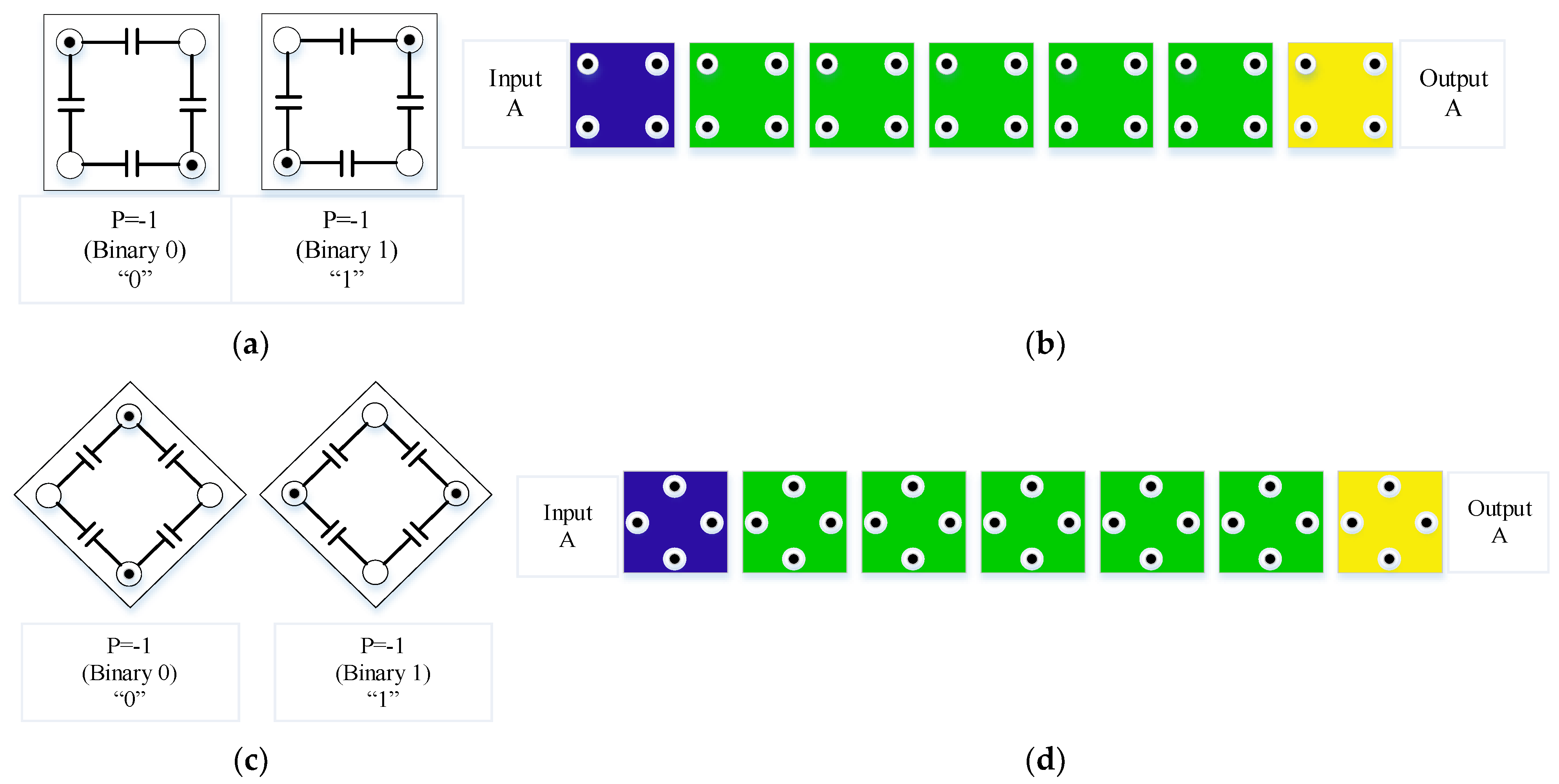
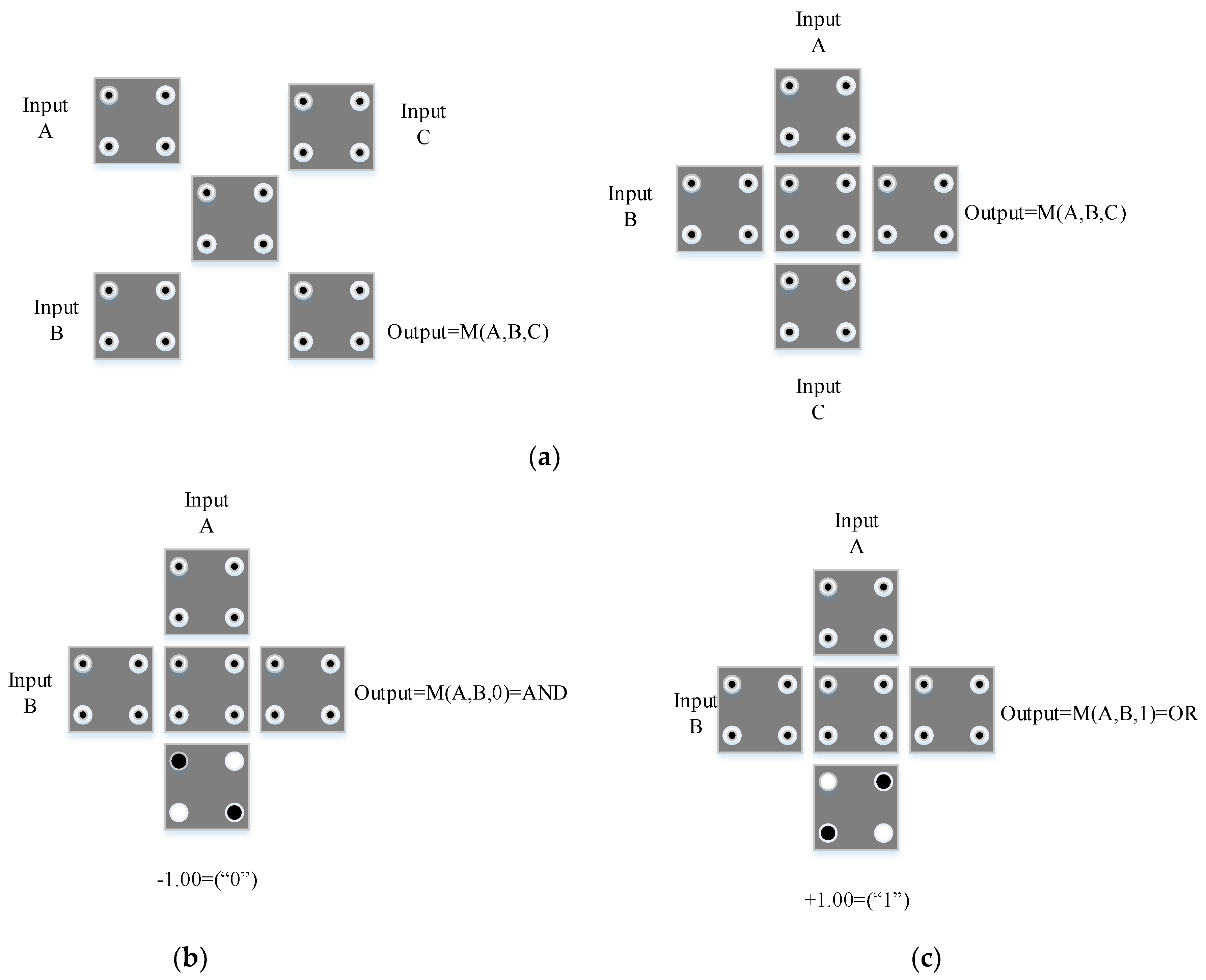
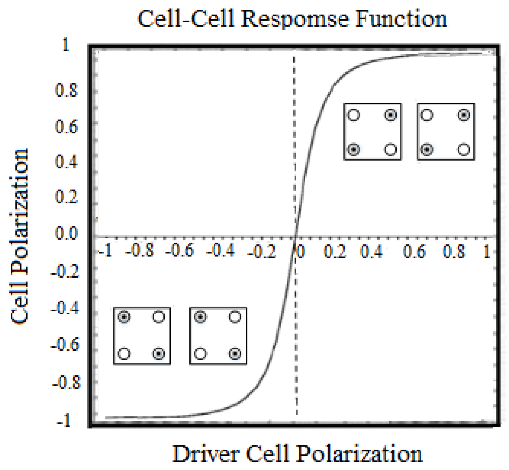
2.1. The Basis of Quantum-Dot Cellular Automata (QCA) Technology

This technology is based on QCA cells, and the basis of the QCA cell can represent a logical bit with occupied space in the nanoscale. A QCA cell includes two electrons, and, based on the Coulombic repulsion created between two electrons, two logical values of “0” and “1” are possible. The QCA cells are square, as shown in Figure 1. Each enclosure consists of four holes. The two electrons are trapped inside and can move freely between the holes; by placing two electrons in four spots, six different states are created, which is impossible due to Coulombic repulsion forces between the electrons. As a result, to satisfy these forces, electrons are placed inside the holes with as far apart as possible, until the Coulombic repulsion law is satisfied. Depending on the location of the electrons and their diameter, two structures are created; by the establishment of two electrons in each of these two poles, two different states are created. With these two types of systems, two logical values can be obtained; we will consider one of the logical values. We attribute these two polar structures 1 and –1 to the logical values of “1” and “0”, respectively; the poles at 1 and –1 same are those of the square cells, as shown in Figure 1 [6,7,8].
When the electrons move inside the cell, they tunnel between the holes. Then, the moving of the electrons inside the cell is similar to a nonlinear move, and the Coulombic repulsion force is not exerted just between the electrons inside a cell. However, as shown in Figure 2, each cell adjacent to this one, which has a logical value, is affected and affects the next adjacent cell that has no value, converting it to its value [6,7,8].

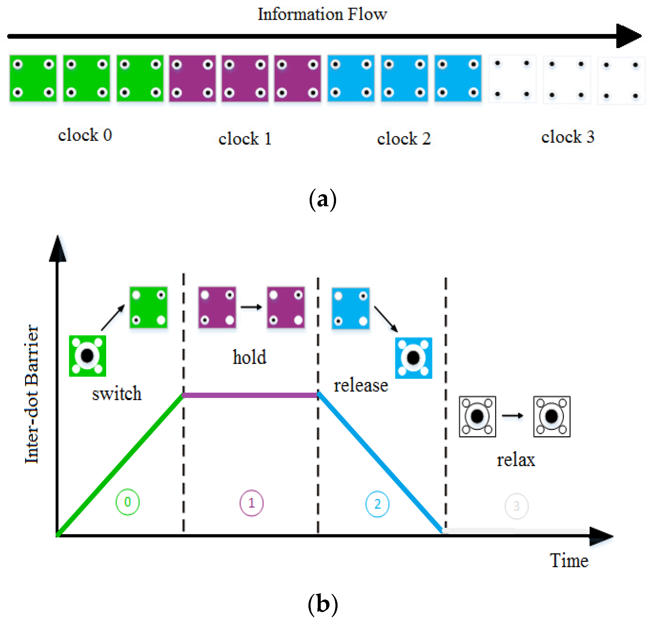
2.2. QCA Four-Phase Clock

A four-clocking phase scheme for the QCA is shown in Figure 3. As shown in the figure, the barriers (potential barriers) rise during the first clock phase (switch). At the beginning of this phase, the borders are low, and the QCA cell is unpolarized; in this state, under the effect Columbic repulsion, the cell receives data from its adjacent cells. Then, with the barriers rising, the QCA cells are polarized according to their input drive modes, and at the end of this clock phase, the borders are high enough to prevent electron tunneling. As a result, the cell is locked. It is in this phase that the actual switching happens. During the second phase of the clock (hold), the barriers remain high. In this phase, the cell is relatively stable and transmits its data to the adjacent cells. The walls gradually decrease during the third clock phase (release), and the cell becomes unstable. In this phase, the cell is allowed to lose its polarization (unpolarized). During the fourth clock phase (relax phase), the cell barriers are in the lowest state, and the cells remain unpolarized. The cell is not used in this phase. After the end of this phase, the cell enters the switch phase again [3,9].

2.3. QCA Four-Phase Clock

One of the gates used in logic circuits is the inverter gate (Not gate). A type of inverter gate used in QCA technology is shown in Figure 4. It is used for inverting the desired signal as required [10,11].
One of the most usable logic gates in QCA technology is the majority gate. This gate has an odd number of inputs and one output. In other words, the output cell value (output cell polarization) is determined according to the logical value of the majority inputs. As a result, the output cell value is determined based on the majority of inputs [8,10]. Figure 5a shows an example of this gate.
By stabilizing (fixed) one of the inputs of the majority gate and considering a logical value “0” (polarization −1), the AND gate is generated [10,12]. Figure 5b shows a two-input AND gate.
The OR gate is generated by fixing one of the majority gate inputs and considering a logical value “1” (polarization +1) [10,12]. Figure 5c shows a two-input OR gate.

2.4. Related Work

In a previous paper [13], the architecture of a Full Adder/Full Subtractor with a multilayer crossover design was described (Figure 6). This type of multilayer design requires a larger consumption area than we planned. It has also more cells and delays with respect to our designs, so its cost is very high. As a result, our proposed technique was implemented using the coplanar method. It has significant advantages over this type of architecture regarding cell number, delay, and area consumption.
In another paper [14], the architecture of a Full Adder/Full Subtractor was also presented (Figure 7). This type of design, due to the high delay and unsuitable carry output, requires another crossover. That leads to an increase in the delay and number of cells. As a result, this architecture is also not suitable. Our proposed design has significant advantages relative to this design [14], such as the number of cells, delay, area of consumption, and therefore cost function.
Another paper [15] described a Full Adder/Full Subtractor architecture using the coplanar method design (Figure 8). This type of design is not very favorable, because the rotated cells (45° cells) make it more vulnerable and increase the implementation costs. Our method has significant advantages also relative to this design [15], such as the number of cells, delay, and area. Besides, normal cells were used. Our design (C) is 50% better than that design.
In a paper [16], a Full Adder/Full Subtractor circuit architecture, implemented in a coplanar method design was presented. Our proposed designs (A and B) are an addition to the coplanar designs in terms of number cells, area and, therefore, cost of implementation and have significant advantages relative to this design (Figure 9). Despite not using rotated cells in our designs (A and B), their latency is equal to that reported in this previous article. In comparison, our third design delay (C) is 33.34% superior to this design and is ideal in terms of cell number and area.
Another paper [17] also presented two Full Adder/Full Subtractor circuit designs, as shown in Figure 10 and Figure 11; these designs are also coplanar, but our designs have significant advantages in terms of number of cells, delay, and area.

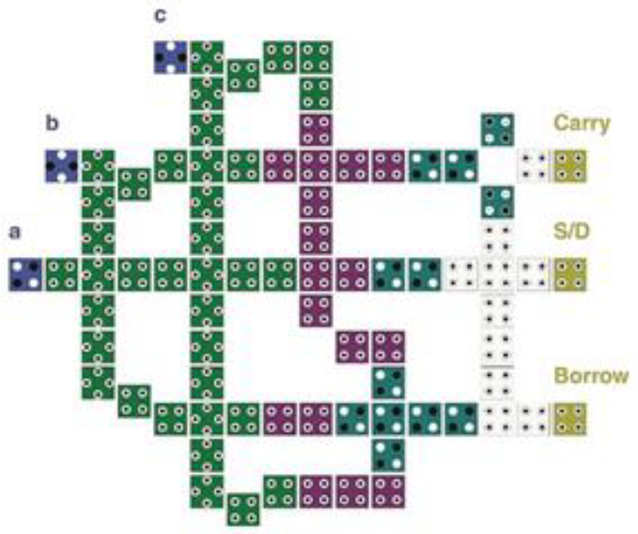
3. The Proposed Circuits

In this paper, we designed three new Full Adder/Subtractor (FA/S) circuits based on the XOR gate [18] with the lowest number of cells, smallest consumption circuit area, and lowest latency (delay) relative to the previous best circuits. In cases, a single-layer (coplanar) design was used. Therefore, these circuits are the best examples of design ever made. The two designs (A and B) are coplanar and use only standard cells (90° cells). In the third design (C) which is coplanar, the cells are rotated (45° cells) and also coplanar. The third design shows that the use of this type of cell may reduce the delay of circuit outputs, but, it also reduces the stability and resistance of the circuit compared to the circuits with standard cells.

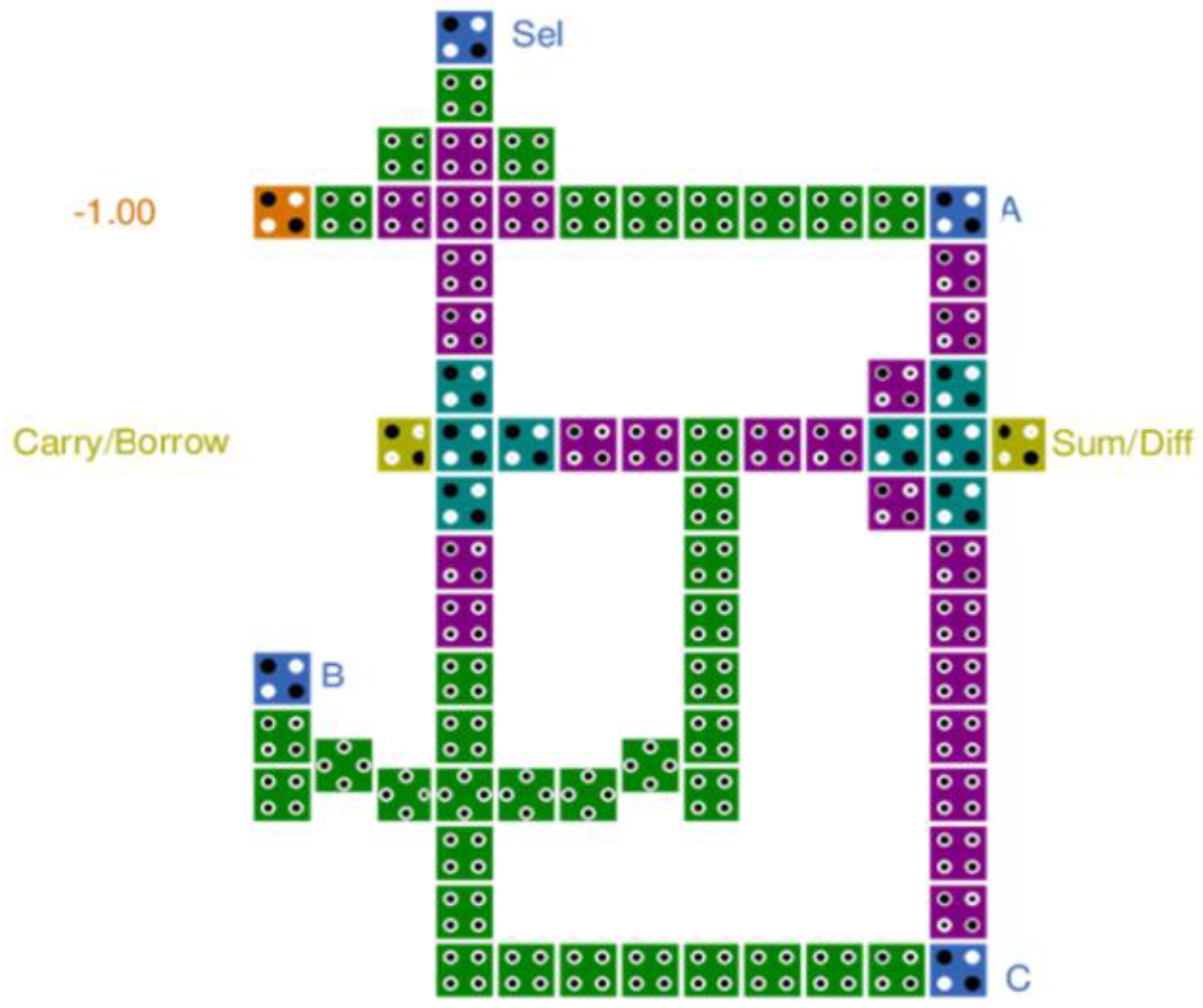
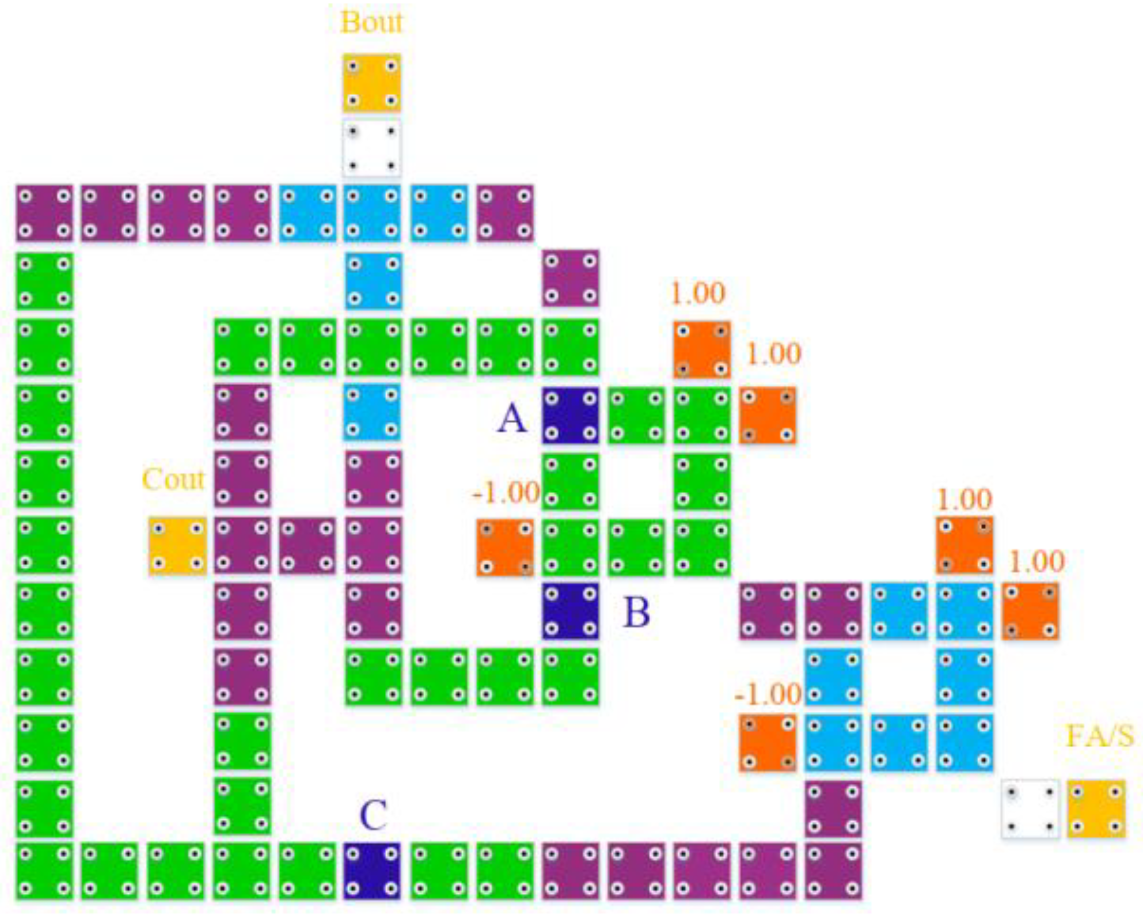
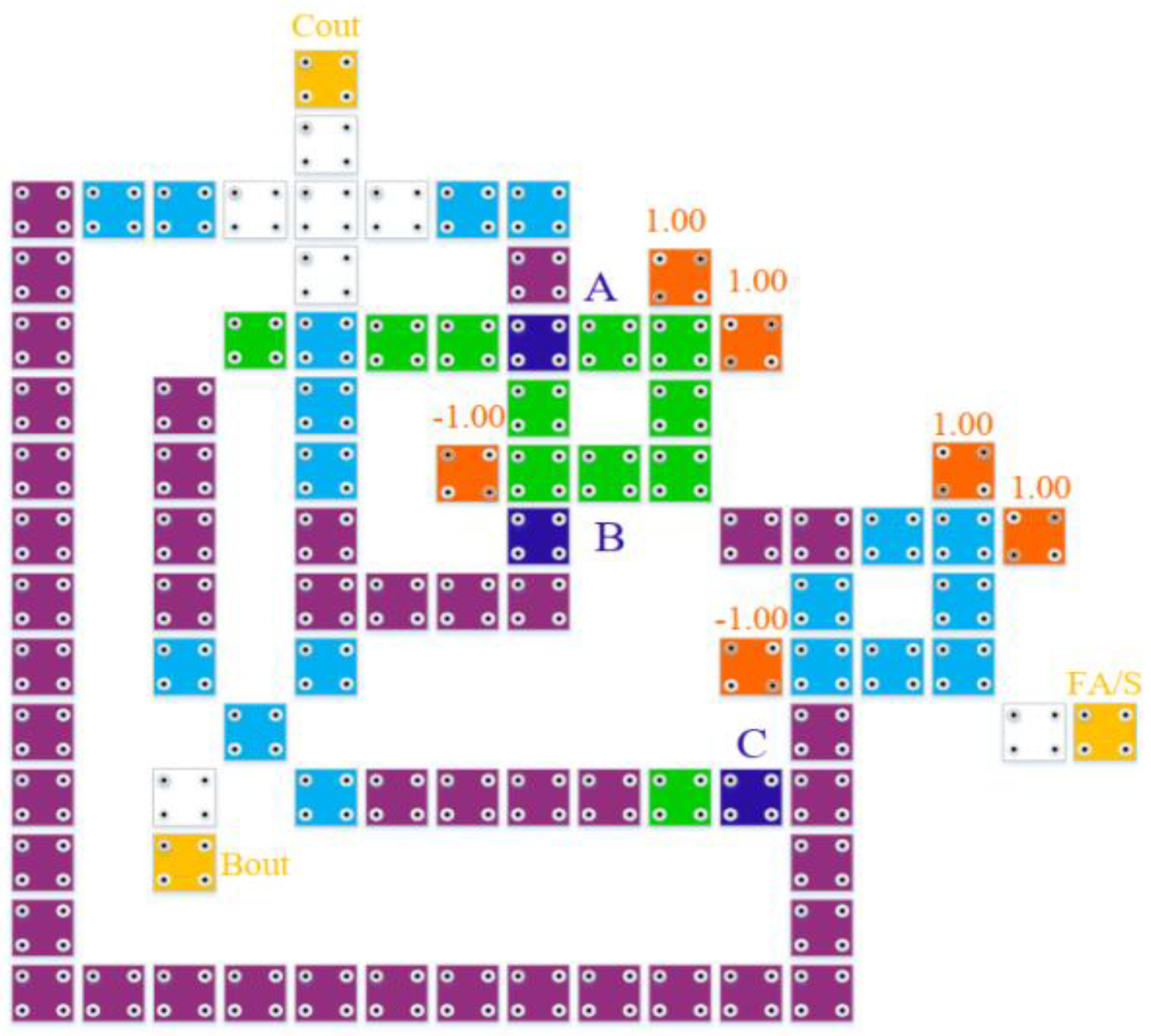
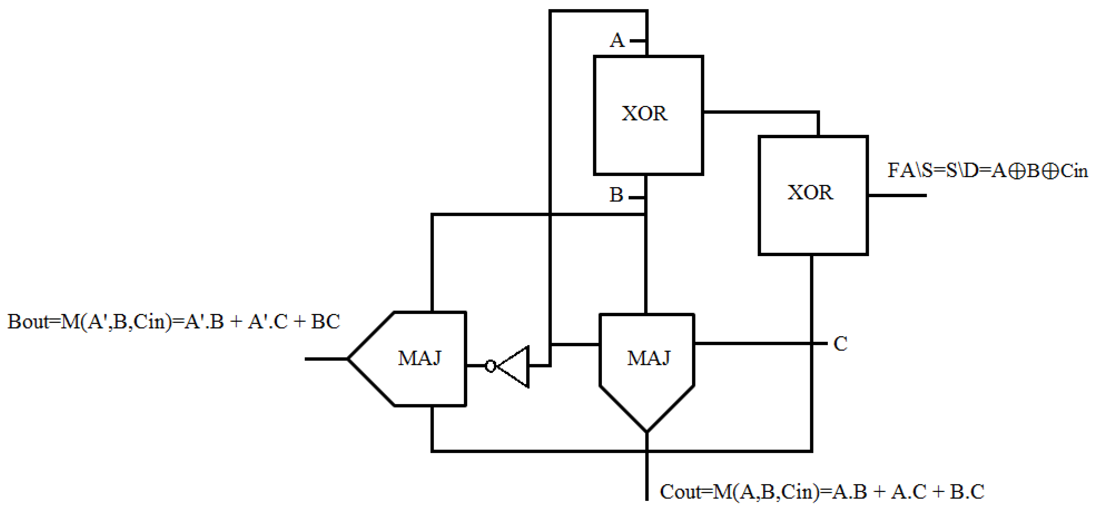
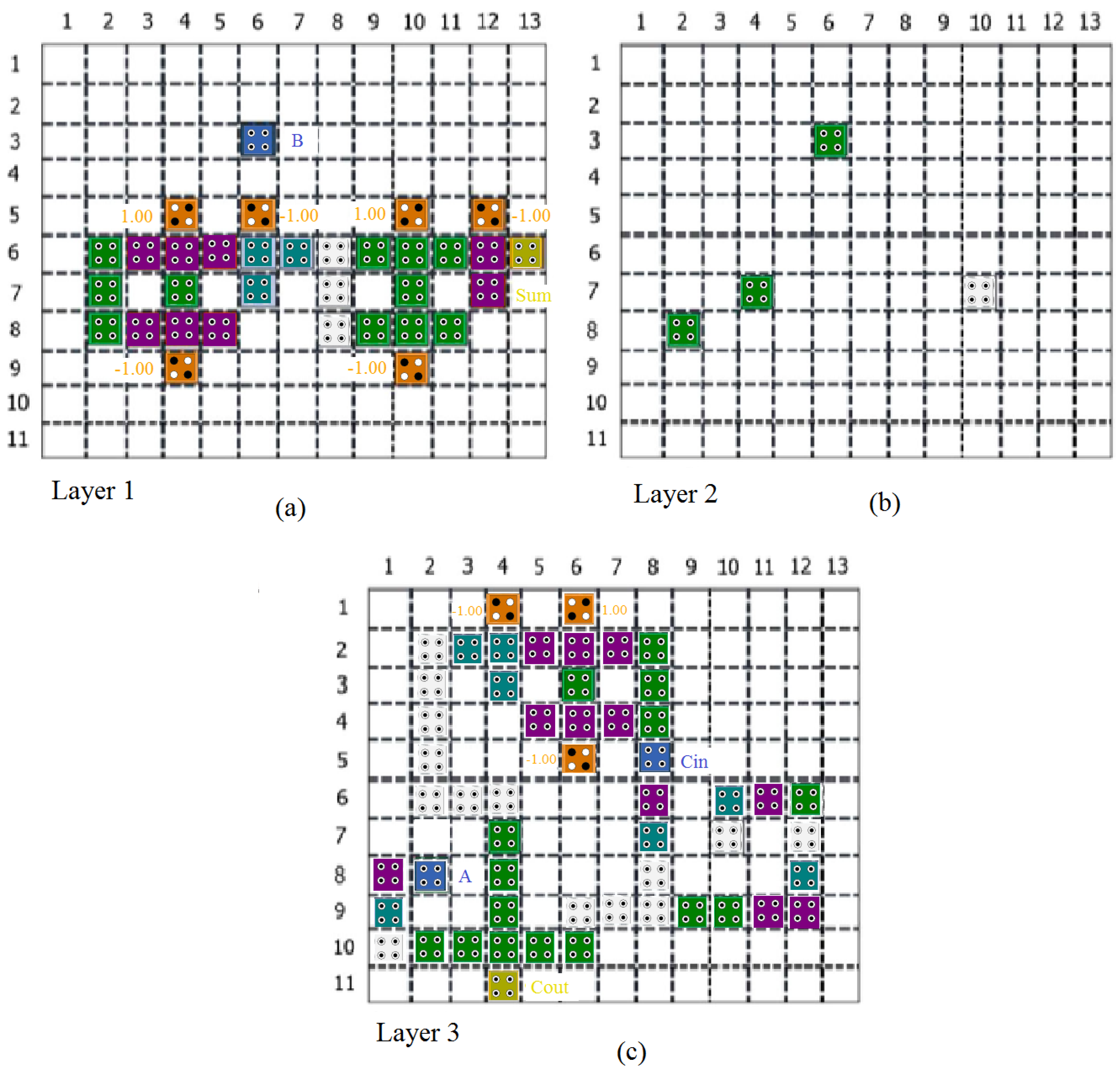
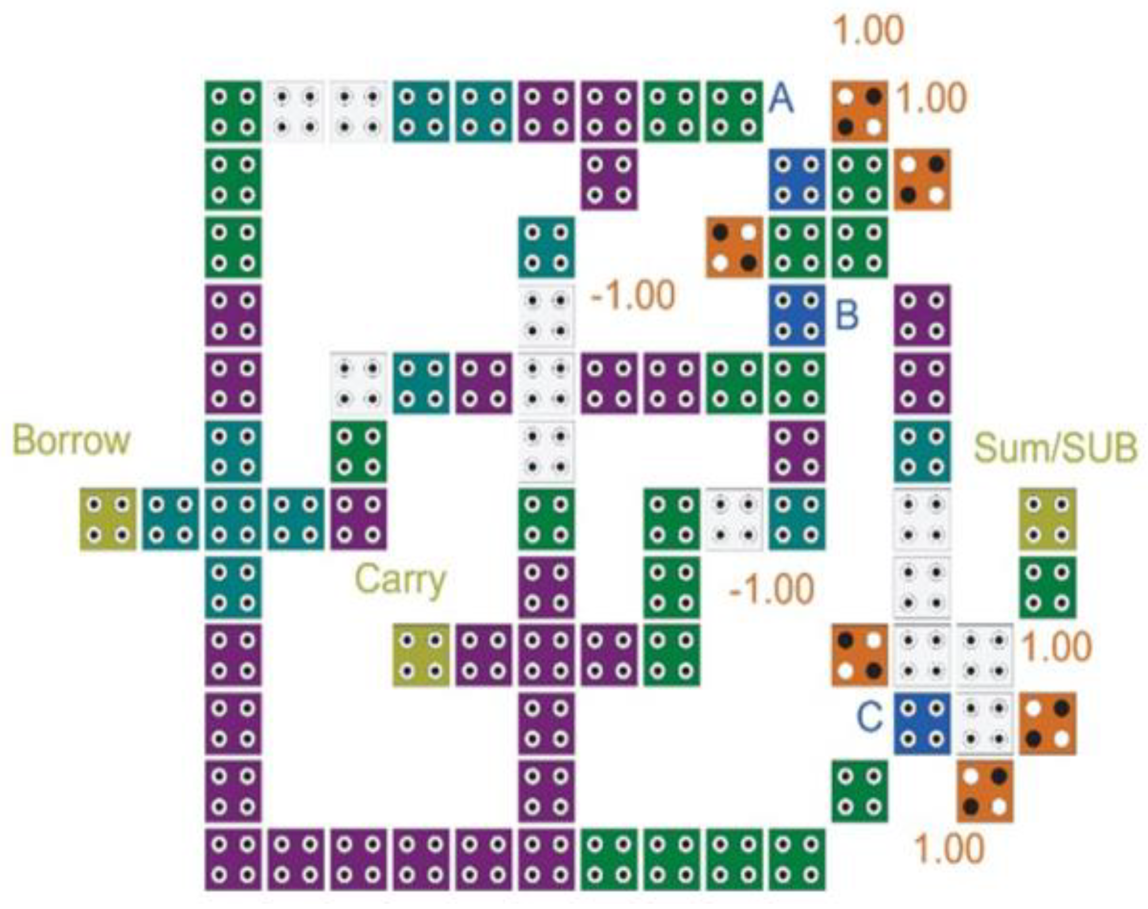
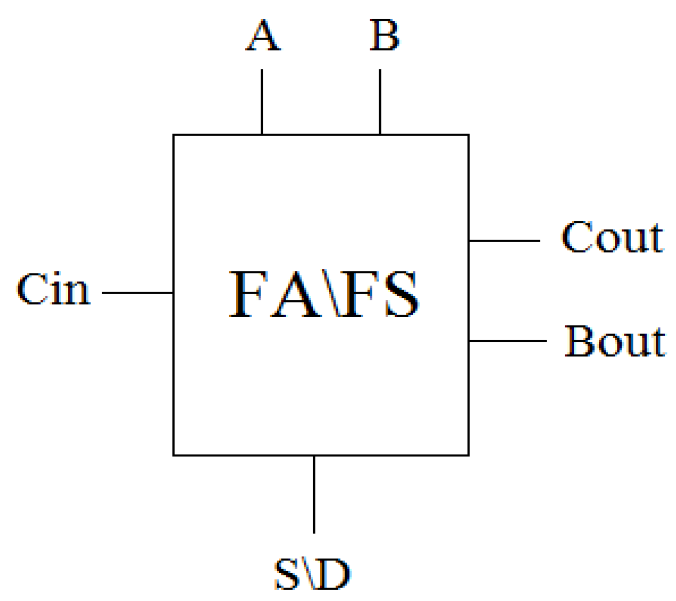
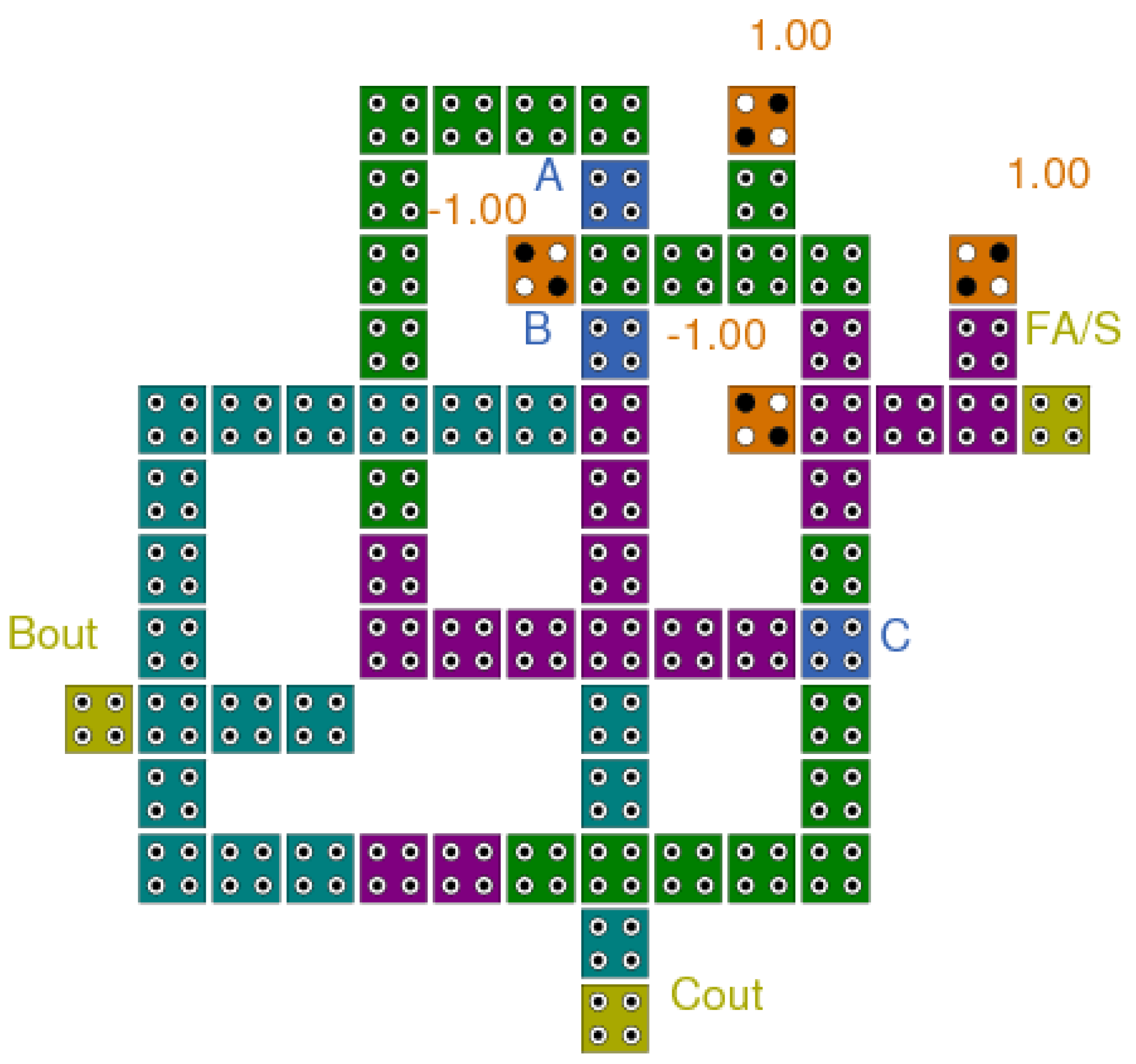
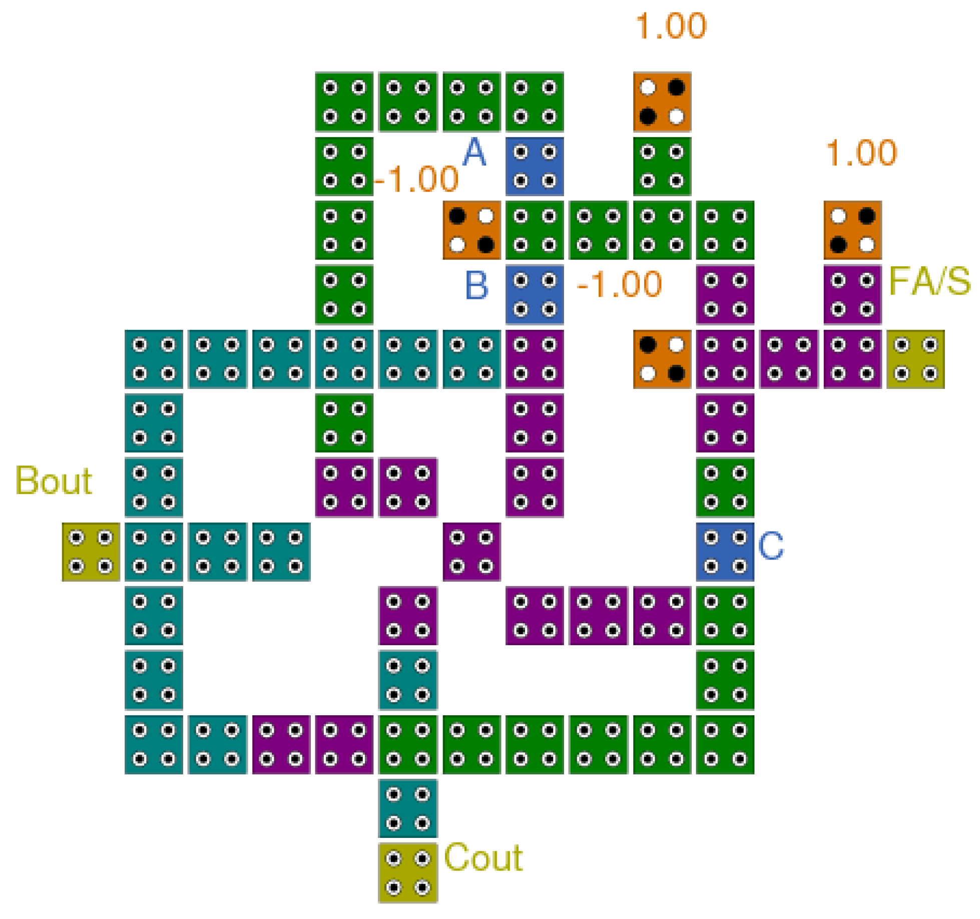
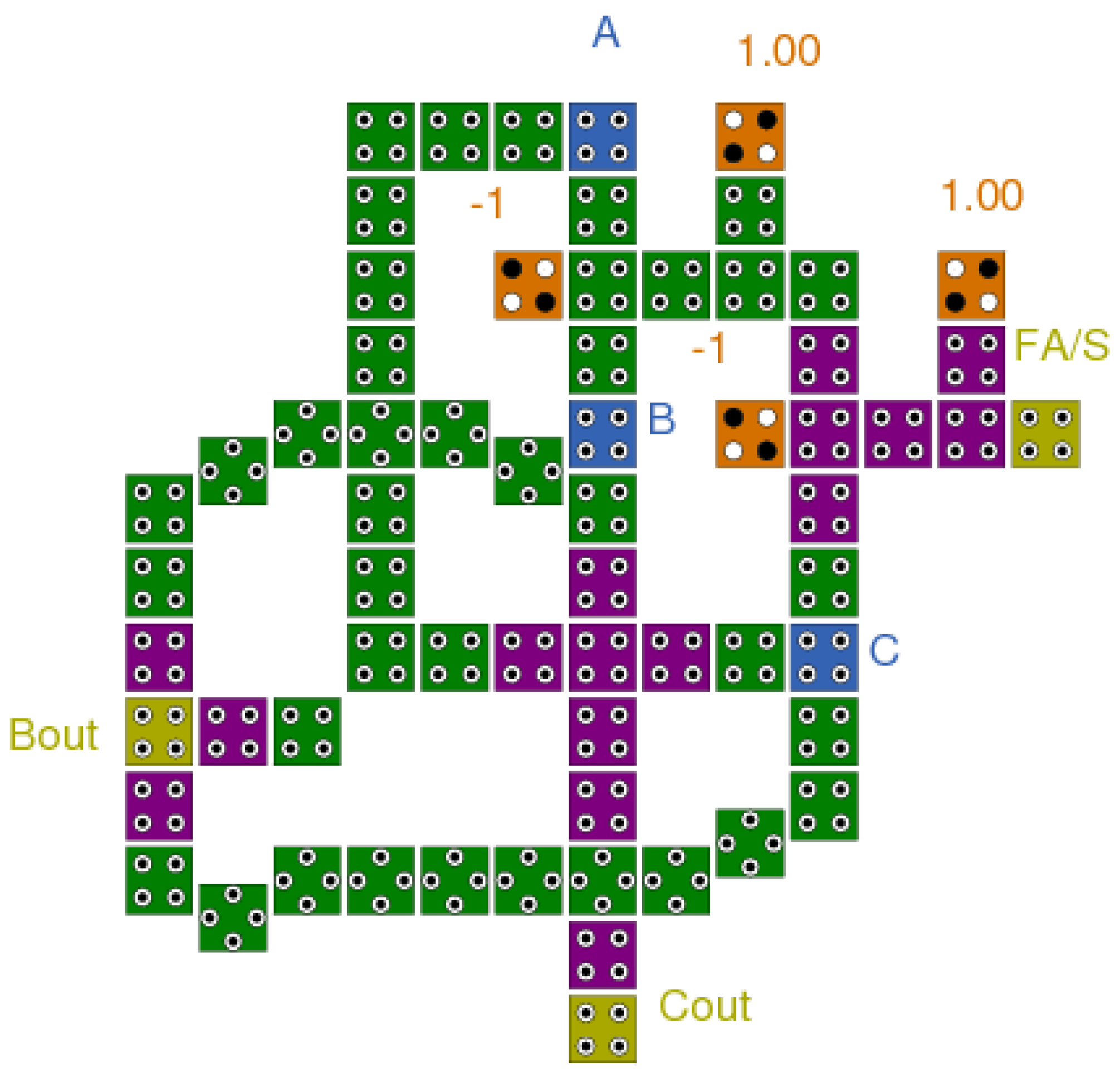
3.1. FA/S Circuits Design

A Full Adder/Subtractor circuit is a combination circuit where two addition and subtraction operations are performed. This circuit has three inputs (A, B, Cin) and three outputs (S\D, Cout, Bout) [19,20]. Equation (1) is the equation of the output S\D, Equation (2) is the equation of the Cout output, and Equation (3) is the equation of the Bout output. Figure 12, block diagram, and Table 1 show the correct Table of this circuit.
S\D = A⊕B⊕Cin
Cout = M(A,B,Cin) = A.B + A.C + B.C
Bout = M(A′,B,Cin) = A′.B + A′.C + B.C
This paper designed FA/S circuits with the lowest number of cells, lowest consumable area, and lowest latency (delay), compared to the previous best examples. We used a single-layer (coplanar) design to obtain the best designs ever made. The design is better than previous ones not only in terms of cell number, area, and delay but also because it is based on a single layer. Figure 13 presents a block diagram of these circuits and Figure 14, Figure 15 and Figure 16, show the implementation of the Proposed Full Adder/Subtractor (FA/S) circuits designs.

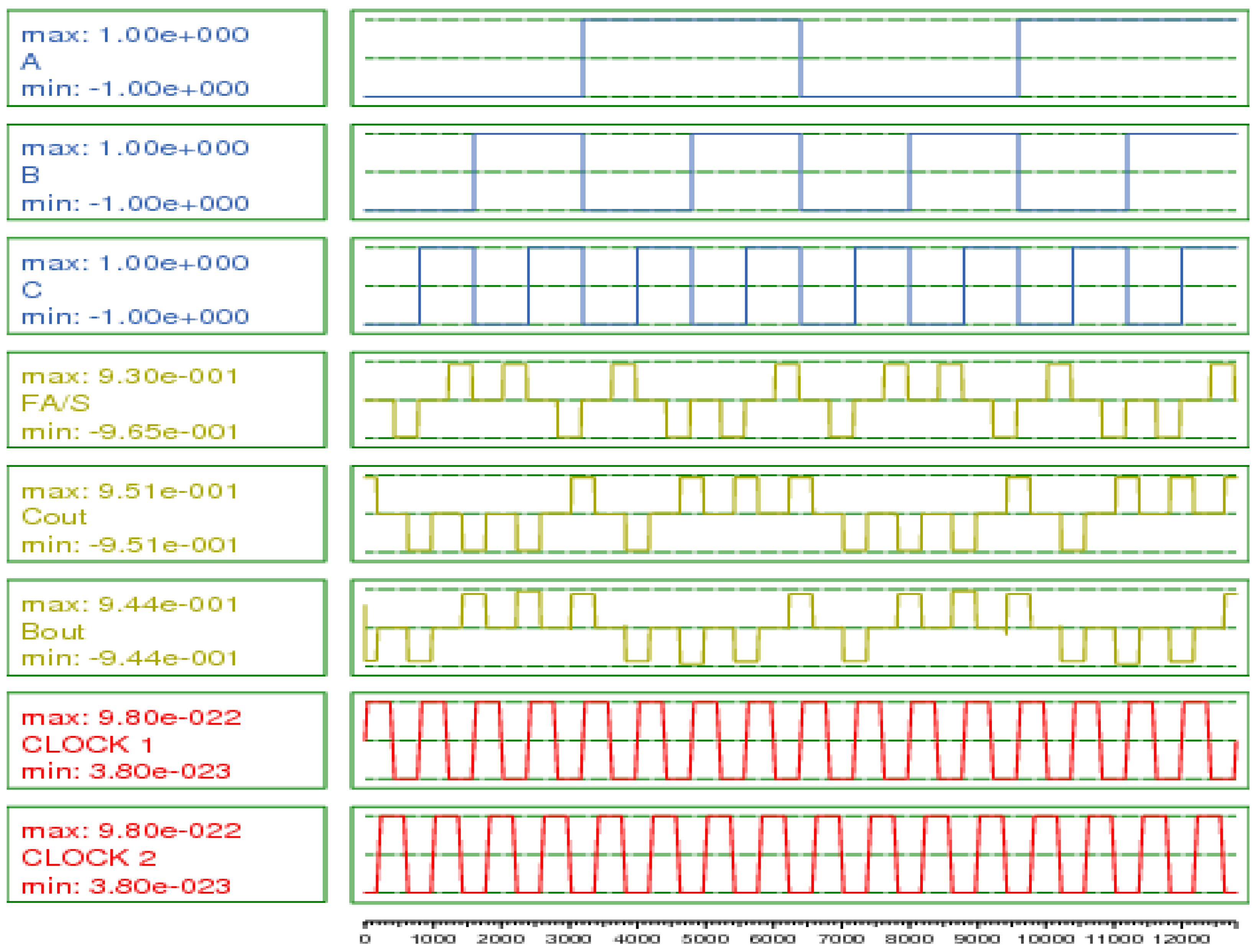
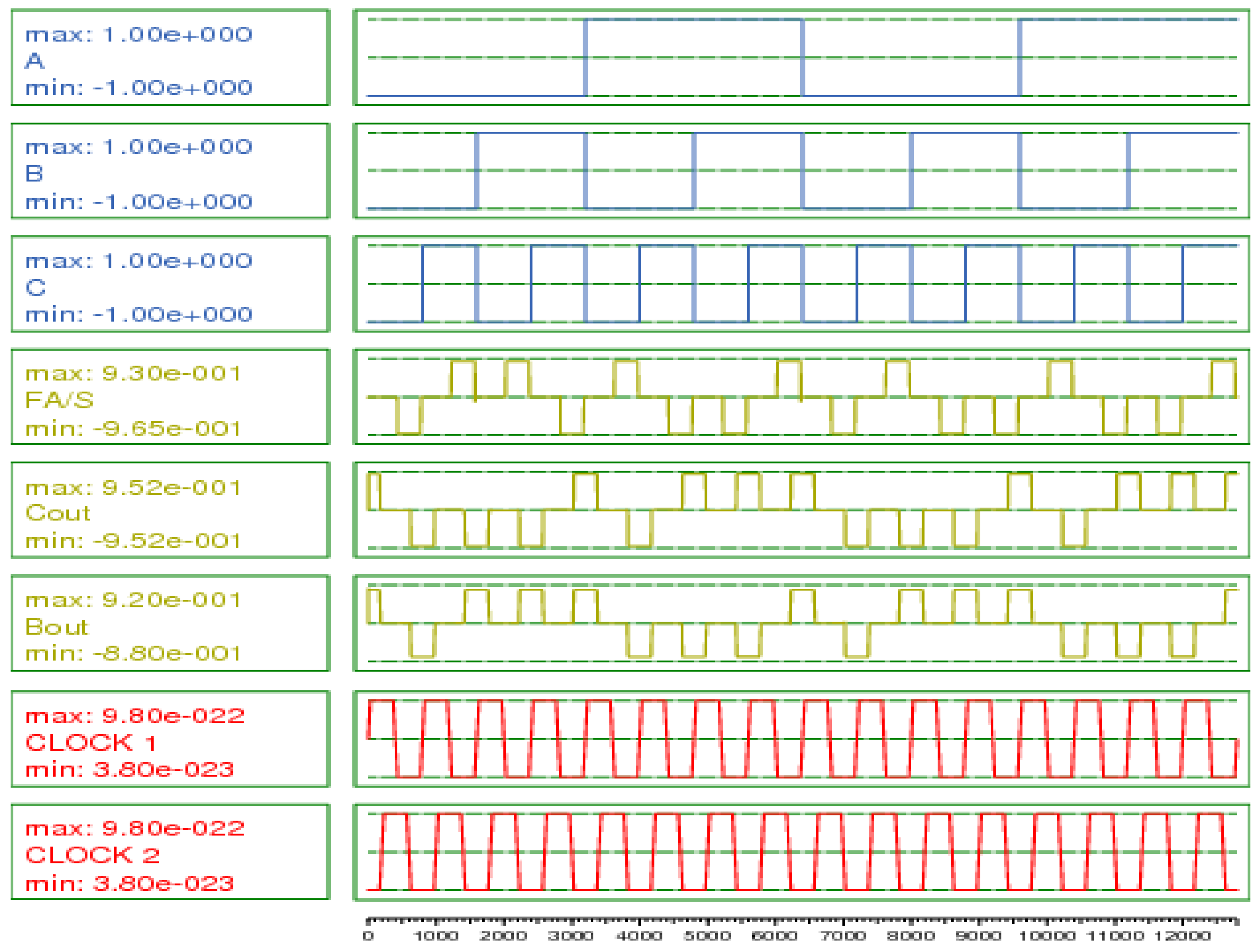
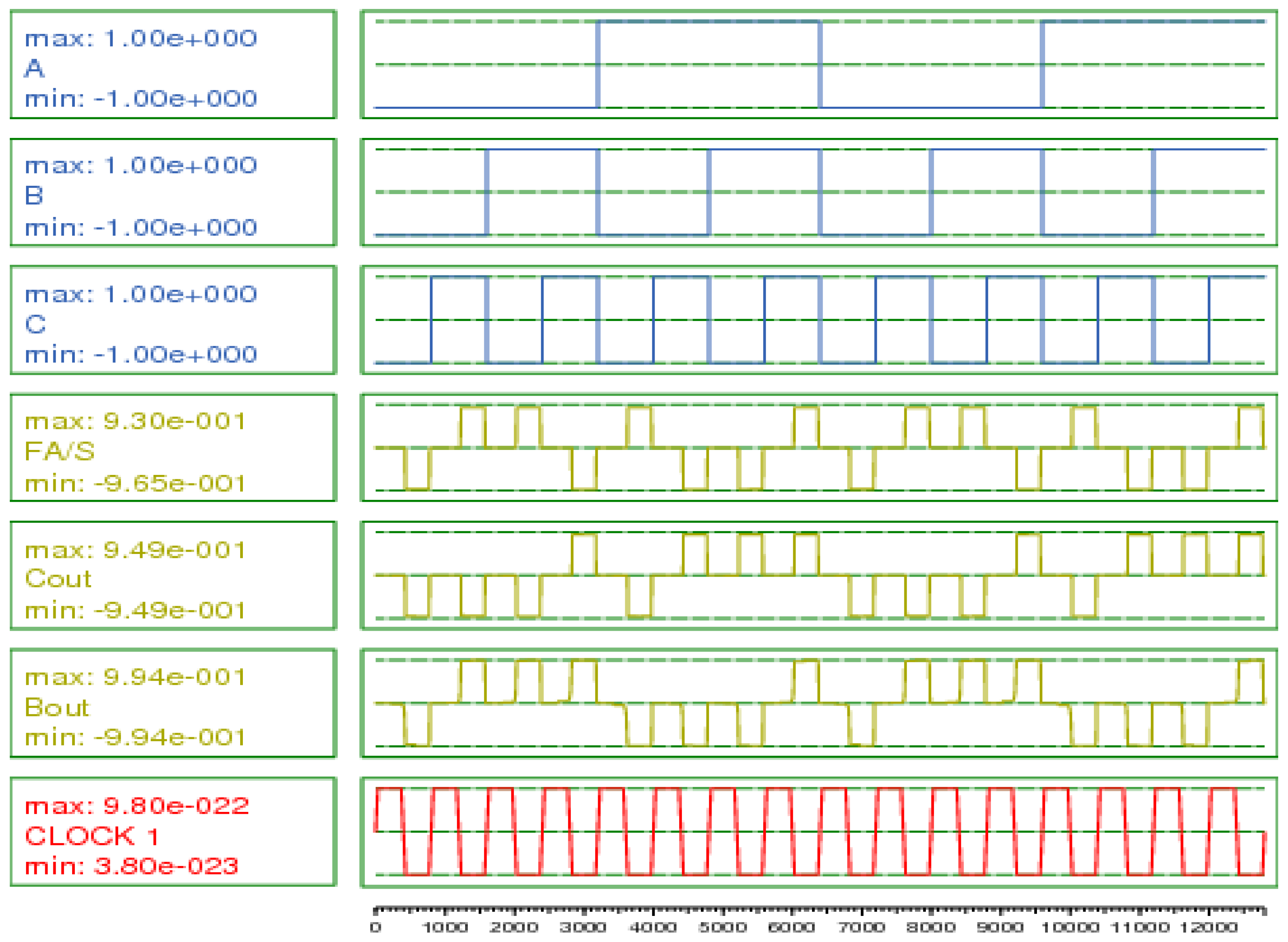
3.2. Simulation Results

In this section, the simulator outputs of the proposed circuits are shown in Figure 17, Figure 18 and Figure 19. The output latency of both offered courses (A and B) is the same, and they provide the same simulation outputs. As can be seen, in both circuits, the delay is one clock (four phases). The delay of the third circuit (C) is 0.5 clock (two stages). The proposed Full Adder/Subtractor hybrid circuits combine two addition and subtraction circuits and allow the concurrent performance of both operations.

4. Guidelines of Performance Evaluation

The QCA Designer provided the simulation results. The simulation parameters are presented in Table 2. The proposed design was compared with designs described in previous works. For all circuits designed, parameters including area, delay, and cell numbers are provided. The type of crossover is also presented for a better and more accurate comparison.
The simulation results are given in Table 3. As can be seen, the proposed circuits were compared with the best circuits previously described. In Table 3, consumption area, delay, and cell number of the proposed Full Adder/Subtractor circuits are compared to those of previous designs.
As shown in Table 3, our designs (A) and (B) allow reducing the area and power consumption up to 39.1% with respect to previous circuits described in [14,17]. As can be seen, the delay in the proposed designs improved significantly with respect to previous works. Our designs (A) and (B) reduce the delay by 50% in comparison to the designs in [13,14] and by 30% with respect to those in [15,17]. The reduction in the proposed design C, relative to the designs in [13,14], corresponds to 66.66%, whereas it corresponds to 50% in comparison to those in [15], [17]-a and [17]-b, and to 33.33% in comparison to that in [16]. As can be seen, the proposed designs have also the lowest cell number with respect to the other designs. Improvement in the cell number of the proposed design A relative to the designs in [13,14,15,16,17]-a and [17]-b is about 24.45%, 18.07%, 17.07%, 9.34%, 26.09%, and 19.05% respectively; the cell number improvement in the proposed design B relative to [13,14,15,16,17]-a and [17]-b, respectively, is about 25.56%, 19.28%, 18.29%, 10.67%, 27.17%, and 20.24%; finally, the cell number improvement in the proposed design C relative to [13,14,15,16,17]-a and [17]-b, respectively, is about 27.78%, 21.69%, 20.73%, 13.34%, 29.35%, and 22.62%.

5. Conclusions

The FA/S designs using the QCA technology use at least three layers for the crossover, while several techniques use 45° cells. Indeed, only non-adjacent clock phases (four clock phases) are required to design the crossover in a single layer, which is robust and better. However, the coplanar crossover’s design using rotated cells can reduce delay in the circuit. In some cases, depending on the type of usage, these two types of design can be used. The circuits’ designs proposed in this study are better and preferable than previous designs in terms of number of cells consumed, circuit area, delay, and cost. As a result, these three proposed designs can be used in more extensive and more complex circuits.

Author Contributions

Conceptualization, M.V.; methodology, M.V.; validation, M.V., P.L. and A.N.B.; formal analysis, M.V.; investigation, M.V., P.L. and A.N.B.; writing—original draft preparation, M.V.; writing—review and editing, P.L. and A.N.B.; supervision, P.L. and A.N.B. All authors have read and agreed to the published version of the manuscript.

Funding

This research received no external funding.

Data Availability Statement

Data are contained within the article.

Conflicts of Interest

The authors declare no conflict of interest.

References

  1. Mohammadi, Z.; Mohammadi, M. Implementing a one-bit reversible full adder using quantum-dot cellular automata. Quantum Inf. Process. 2014, 13, 2127–2147. [Google Scholar] [CrossRef]
  2. Tougaw, P.D.; Lent, C.S. Logical devices implemented using quantum cellular automata. J. Appl. Phys. 1994, 75, 1818–1825. [Google Scholar] [CrossRef]
  3. Cho, H.; Swartzlander, E.E. Adder Designs and Analyses for Quantum-Dot Cellular Automata. IEEE Trans. Nanotechnol. 2007, 6, 374–383. [Google Scholar] [CrossRef]
  4. Huang, J.; Momenzadeh, M.; Tahoori, M.B.; Lombardi, F. Design and characterization of an and-or-inverter (AOI) gate for QCA implementation. In Proceedings of the 14th ACM Great Lakes Symposium on VLSI 2004, Boston, MA, USA, 26–28 April 2004; pp. 426–429. [Google Scholar] [CrossRef]
  5. Abedi, D.; Jaberipur, G.; Sangsefidi, M. Coplanar full adder in quantum-dot cellular automata via clock-zone-based crossover. IEEE Trans. Nanotechnol. 2015, 14, 497–504. [Google Scholar] [CrossRef]
  6. Fortes, J.A. Future challenges in VLSI system design. In Proceedings of the IEEE Computer Society Annual Symposium on VLSI, Tampa, FL, USA, 20–21 February 2003; pp. 5–7. [Google Scholar]
  7. Frost, S.E.; Rodrigues, A.F.; Janiszewski, A.W.; Rausch, R.T.; Kogge, P.M. Memory in motion: A study of storage structures in QCA. In Proceedings of the First Workshop on Non-Silicon Computing, Cambridge, MA, USA, 3 February 2002; Volume 2. [Google Scholar]
  8. Wang, W.; Walus, K.; Jullien, G.A. Quantum-dot cellular automata adders. In Proceedings of the 2003 Third IEEE Conference on Nanotechnology, San Francisco, CA, USA, 12–14 August 2003; Volume 1, pp. 461–464. [Google Scholar]
  9. Kianpour, M.; Sabbaghi-Nadooshan, R. Optimized Design of Multiplexor by Quantum-dot Cellular Automata. Int. J. Nanosci. Nanotechnol. 2013, 9, 15–24. [Google Scholar]
  10. Beigh, M.R.; Mustafa, M.; Ahmad, F. Performance Evaluation of Efficient XOR Structures in Quantum-Dot Cellular Automata (QCA). Circuits Syst. 2013, 4, 147–156. [Google Scholar] [CrossRef] [Green Version]
  11. Swartzlander, E.E.; Cho, H.; Kong, I.; Kim, S.W. Computer arithmetic implemented with QCA: A progress report. In Proceedings of the 2010 Conference Record of the Forty Fourth Asilomar Conference on Signals, Systems and Computers, Pacific Grove, CA, USA, 7–10 November 2010; pp. 1392–1398. [Google Scholar]
  12. Modi, S.; Tomar, A.S. Logic gate implementations for quantum dot cellular automata. In Proceedings of the 2010 International Conference on Computational Intelligence and Communication Networks, Bhopal, India, 26–28 November 2010. [Google Scholar]
  13. Barughi, Y.Z.; Heikalabad, S.R. A Three-Layer Full Adder/Subtractor Structure in Quantum-Dot Cellular Automata. Int. J. Theor. Phys. 2017, 56, 2848–2858. [Google Scholar] [CrossRef]
  14. Zoka, S.; Gholami, M. A novel efficient full adder–subtractor in QCA nanotechnology. Int. Nano Lett. 2018, 9, 51–54. [Google Scholar] [CrossRef] [Green Version]
  15. Sadeghi, M.; Navi, K.; Dolatshahi, M. Novel efficient full adder and full subtractor designs in quantum cellular automata. J. Supercomput. 2019, 76, 2191–2205. [Google Scholar] [CrossRef]
  16. Raj, M.; Gopalakrishnan, L.; Ko, S.-B. Design and analysis of novel QCA full adder-subtractor. Int. J. Electron. Lett. 2020, 9, 1–14. [Google Scholar] [CrossRef]
  17. Vahabi, M.; Sabbagh Molahosseini, A. A New Coplanar Full Adder/Subtractor in Quantum-Dot Cellular Automata Technology. Majlesi J. Telecommun. Devices 2018, 7, 53–63. [Google Scholar]
  18. Chabi, A.M.; Roohi, A.; Khademolhosseini, H.; Sheikhfaal, S.; Angizi, S.; Navi, K.; DeMara, R.F. Towards ultra-efficient QCA reversible circuits. Microprocess. Microsyst. 2017, 49, 127–138. [Google Scholar] [CrossRef]
  19. Gladshtein, M. Design and simulation of novel adder/subtractors on quantum-dot cellular automata: Radical departure from Boolean logic circuits. Microelectron. J. 2013, 44, 545–552. [Google Scholar] [CrossRef]
  20. Ahmad, F.; Ahmed, S.; Kakkar, V.; Bhat, G.M.; Bahar, A.N.; Wani, S. Modular design of ultra-efficient reversible full adder-subtractor in QCA with power dissipation analysis. Int. J. Theor. Phys. 2018, 57, 2863–2880. [Google Scholar] [CrossRef]
Figure 1. (a) Normal QCA cells’ structure, (b) Normal QCA wire’s structure, (c) Rotated QCA cells’ structure and (d) Rotated QCA wire’s structure.
Applsci 11 08717 g001
Figure 2. Behavior of adjacent cells.
Applsci 11 08717 g002
Figure 3. (a) Clock phases and (b) QCA four-phase clock mechanism.
Applsci 11 08717 g003
Figure 4. Two different Not-gate in QCA based on 90° cells.
Applsci 11 08717 g004
Figure 5. (a) QCA with implementation of the majority gate, (b) QCA with implementation of the AND Gate with two inputs and (c) QCA with implementation of the OR Gate with two inputs.
Applsci 11 08717 g005
Figure 6. Full Adder/Full Subtractor circuit [13].
Applsci 11 08717 g006
Figure 7. Full Adder/Full Subtractor circuit [14].
Applsci 11 08717 g007
Figure 8. Full Adder/Full Subtractor circuit [15].
Applsci 11 08717 g008
Figure 9. Full Adder/Full Subtractor circuit [16].
Applsci 11 08717 g009
Figure 10. Full Adder/Full Subtractor circuit [17]-a.
Applsci 11 08717 g010
Figure 11. Full Adder/Full Subtractor circuit [17]-b.
Applsci 11 08717 g011
Figure 12. Block diagram of the Full Adder/Subtractor circuit.
Applsci 11 08717 g012
Figure 13. Simulation results of the proposed XOR-gate.
Applsci 11 08717 g013
Figure 14. The proposed (A) Full Adder/Full Subtractor circuit.
Applsci 11 08717 g014
Figure 15. The proposed (B) Full Adder/Full Subtractor circuit.
Applsci 11 08717 g015
Figure 16. The proposed (C) Full Adder/Full Subtractor circuit.
Applsci 11 08717 g016
Figure 17. Simulation results for the proposed (A) Full Adder/Full Subtractor circuit.
Applsci 11 08717 g017
Figure 18. Simulation results for the proposed (B) Full Adder/Full Subtractor circuit.
Applsci 11 08717 g018
Figure 19. Simulation results for the proposed (C) Full Adder/Full Subtractor circuit.
Applsci 11 08717 g019
Table 1. Truth table of the Full Adder/Subtractor.
BoutCoutS\DCinBA
000000
101100
101010
110110
001001
010101
010011
111111
Table 2. Simulation parameters for the QCA Designer.
ParameterValue
Cell width18 nm
Cell height18 nm
Dot diameter5 nm
Number of samples12,800
Convergence tolerance0.001
Radius of effect65 nm
Relative permittivity12.9
Clock high9.8 × 10−22 J
Clock low3.8 × 10−23 J
Clock amplitude factor2
Layer separation11.5 nm
Maximum iteration per sample100
Table 3. Comparing the Full Adder/Subtractor (FA/S) of this study with those of previous works.
Crossover TypeLatency
(clock)
Cell CountArea
(µm2)
Circuit
Multi-Layer1.5900.6[13]
Coplanar (clocking based)1.5830.09[14]
Coplanar (rotated cells)1820.11[15]
Coplanar (rotated cells)0.75750.09[16]
Coplanar (clocking based)1920.09[17]-a
Coplanar (clocking based)1840.09[17]-b
Coplanar (clocking based)0.75680.072Proposed A
Coplanar (clocking based)0.75670.072Proposed B
Coplanar (rotated cells)0.5650.067Proposed C
Publisher’s Note: MDPI stays neutral with regard to jurisdictional claims in published maps and institutional affiliations.

