Article

Design of Power Splitters Based on Hybrid Plasmonic Waveguides

1
College of Science, Henan University of Technology, Zhengzhou 450001, China
2
Department of Applied Physics and State Key Laboratory for Modification of Chemical Fibers and Polymer Materials, Donghua University, Songjiang District, Shanghai 201620, China
3
National Laboratory for Infrared Physics, Shanghai Institute of Technical Physics, Chinese Academy of Sciences, 500 Yutian Road, Shanghai 200083, China
*
Authors to whom correspondence should be addressed.
Appl. Sci. 2021, 11(18), 8644; https://doi.org/10.3390/app11188644
Submission received: 6 August 2021 / Revised: 14 September 2021 / Accepted: 15 September 2021 / Published: 17 September 2021
(This article belongs to the Special Issue Recent Advances in Silicon Photonics Design)

Abstract

:
Plasmonic power splitters based on hybrid plasmonic waveguides (HPWs) are proposed and investigated. The HPW consists of a high-permittivity semiconductor nanowire embedded in a SiO2 dielectric film near a metal surface. The propagation behaviors of Surface Plasmon Polaritons (SPPs) in HPWs are numerically simulated by the 3D finite-difference time-domain (FDTD) method. The incident field is transferred from the middle waveguide to the waveguides on both sides due to the coupling between adjacent waveguides. The intensity distributions can be explained by the multimode interference of SPPs supermodes. According to the field intensity distribution of five HPWs, we design a 1 × 3 power splitter and a 1 × 2 power splitter by reducing the length of some specific waveguides.

1. Introduction

Surface Plasmon Polariton (SPP) waveguides can break the diffraction limitation and are regarded as the best candidate to design miniaturized photonic integrated circuits [1,2]. All kinds of plasmonic waveguides have been designed, such as the dielectric loaded metal, metal wedges, slot and gap waveguides, and hybrid plasmonic waveguides [3,4]. Among these plasmonic waveguides, the hybrid plasmonic waveguide (HPW) is one of the most promising alternatives for on-chip nanophotonics due to the ability of subwavelength confinement and long propagation lengths [3].
In photonic integrated circuits, a power splitter is an essential component, which can distribute the energy of incident light to different propagation directions. Various plasmonic power splitters have been proposed, such as 1 × 2 splitters [5,6,7,8], 1 × 3 splitters [9], 1 × N splitters [10,11,12], and variable transmission splitters [13,14,15]. The overwhelming majority of these plasmonic splitters are designed on the basis of metal–insulator–metal (MIM) waveguides, which are composed of two metallic layers and a dielectric layer [5,6,7,8,9,10,11,12,13,14,15]. However, there are few researches on the power splitter based on HPWs. The main reason is that an MIM waveguide could be simplified to a two-dimensional structure and a HPW cannot be simplified to a two-dimensional structure, of which the computational complexity of a 3D structure is much larger than that of a 2D structure. Due to the excellent performance of the HPWs, it is necessary to design a 3D power splitter based on HPWs for the next generation of integrated photonic circuits.
In this paper, we present several new power splitters based on hybrid plasmonic waveguides. The propagation behaviors of Surface Plasmon Polaritons (SPPs) in HPWs are numerically simulated by the 3D finite-difference time-domain (FDTD) method. According to the field distribution of five HPWs, we reduce the length of some specific waveguides and design different types of power splitters. The power splitters based on HPWs are fully compatible with semiconductor fabrication techniques and can be widely used in integrated photonics structures.

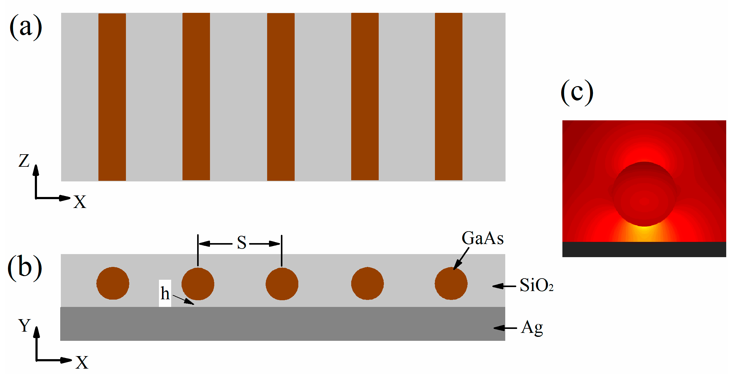
2. Materials and Methods

The hybrid mode in the single HPW was discussed in detail in ref. [3]. Here, we considered a coupled system composed of five HPWs, shown in Figure 1. The HPW consists of a high-permittivity semiconductor nanowire embedded in a low-permittivity dielectric near a metal surface [3]. The semiconductor nanowire was GaAs, of which the relative permittivity is 12.25. The low-permittivity dielectric was SiO2, with relative permittivity 2.25. The relative permittivity of Ag was taken to be the measured value of ε = −129 + 3.3j at the telecommunications wavelength λ = 1550 nm [16]. The diameter of the GaAs nanowire was d = 200 nm and the dielectric gap was h = 50 nm. The distance between adjacent waveguides was S = 500 nm. The plasmonic mode supported by a single HPW is shown in Figure 1c, which was consistent with the results of ref. [3].
We numerically simulated the propagation behavior of SPPs in five HPWs by the 3D FDTD method. The grid size was dx = dz = 10 nm and the time increment was Δt = Δs/2c. A perfectly matching layer was adopted to absorb the outgoing electromagnetic wave around the computational domain.

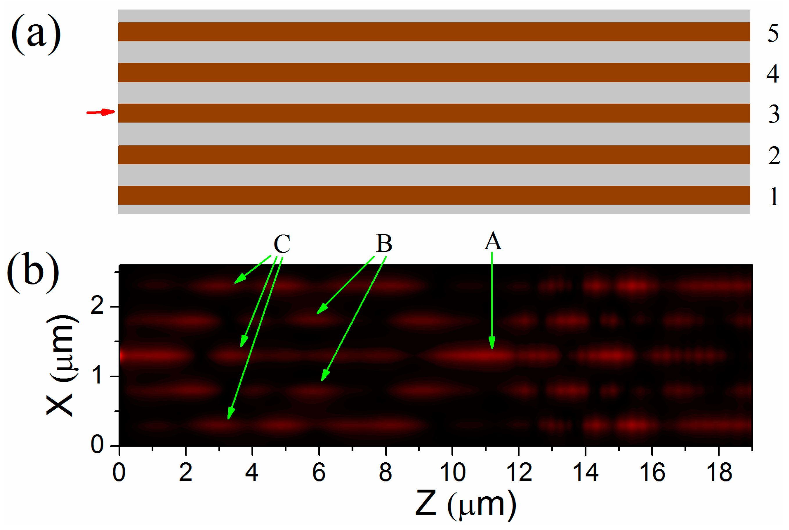
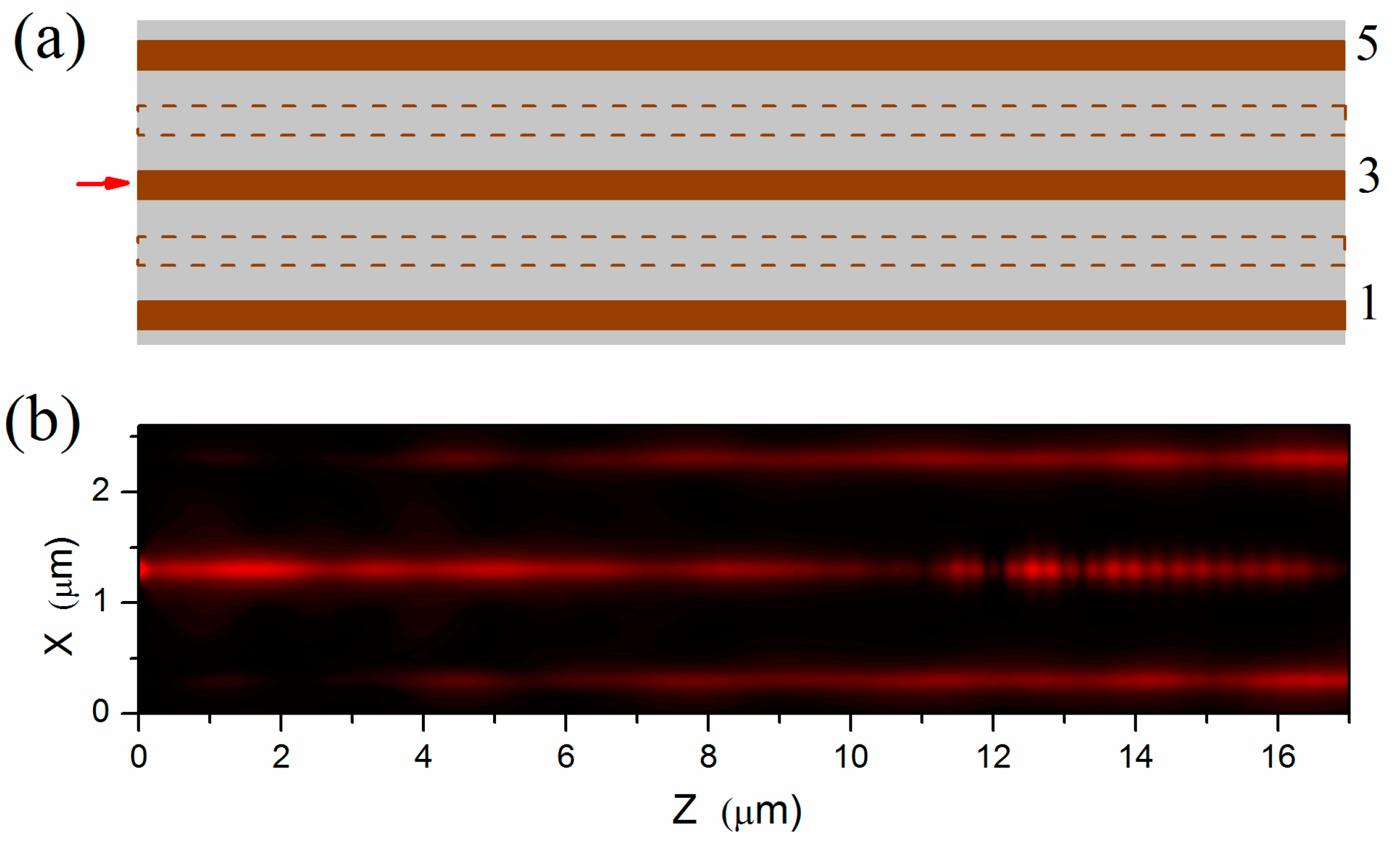
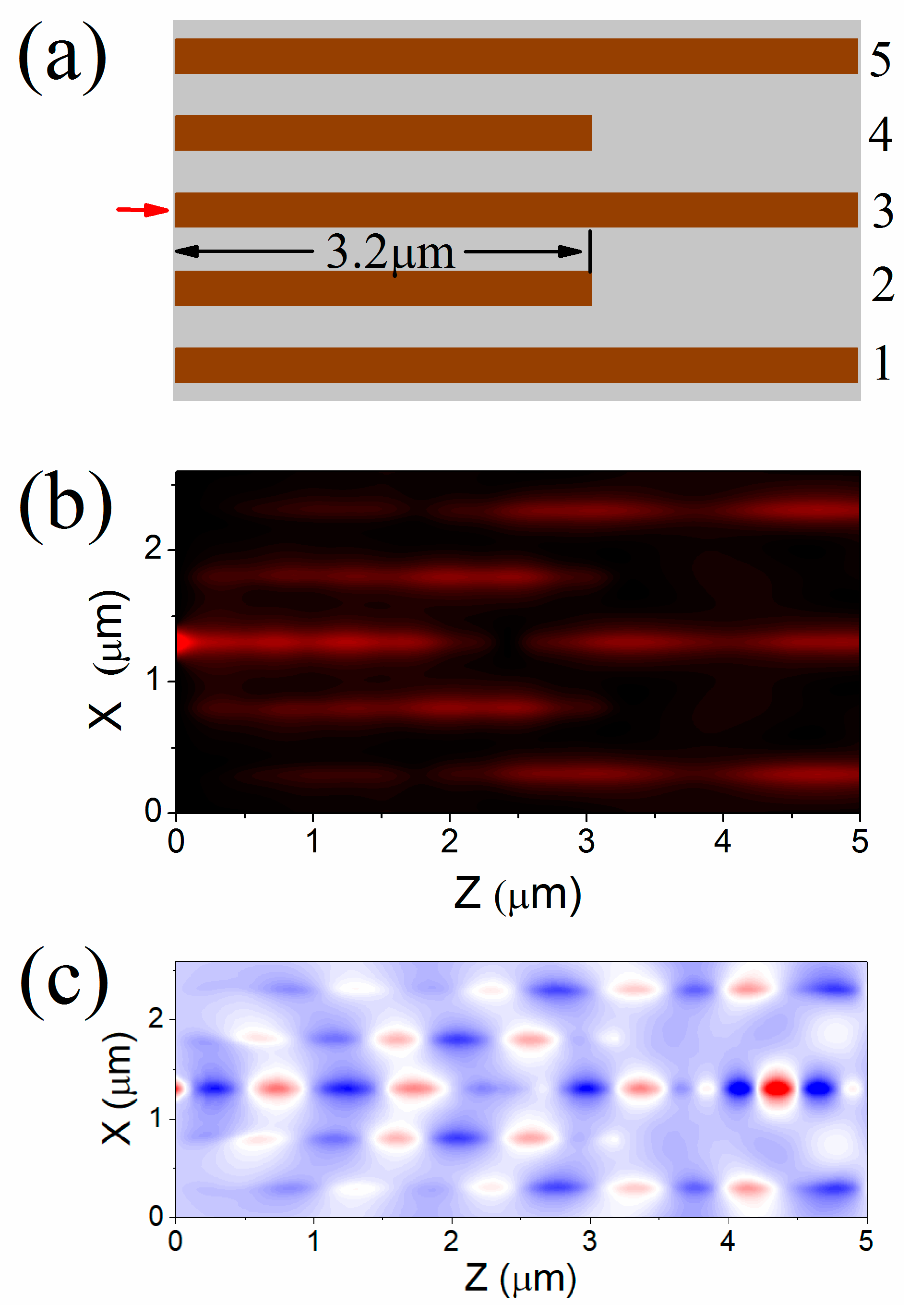
3. Results and Discussion

The plasmonic mode was excited by a Gaussian beam, which is normally focused onto the end of the middle waveguide [17]. The arrangement of the five HPWsis shown in Figure 2a. The intensity distributions in the XZ plane are shown in Figure 2b, where the pattern was very complex due to multimode interference effects [18]. In ref. [18], the principles and properties of multimode interference devices are presented for conventional dielectric waveguides. To the device of five HPWs, supermodes were formed due to the coupling between adjacent waveguides [19,20]. Customarily, supermodes are the modes of propagation of a periodic array of waveguides, which consists of N identical waveguides [20].
The wave functions of the supermodes were written as linear combinations of the unperturbed wave functions of the individual waveguides:
H s ( x , z ) = n = 1 N C s , n ψ n ( x , z )
The total field in a periodic array of waveguides can be expressed as a sum of all supermodes, which can be written as:
φ ( x , z ) = s = 1 N a s H s ( x ) e i β s z
β s is the propagation constant of a single supermode, a s is the weight coefficient of excited supermodes [19].
Due to the incident field of SPPs being the input from the middle waveguide, even supermodes can be excited. These excited supermodes produced a multimode interference and formed a self-imaging phenomenon. The corresponding N-fold images were expected to form at distances [18]:
L = P N ( 3 L π 4 )   ( P   =   1 ,   2 ,   3 ,   )
where P denotes the periodic nature of the imaging along the waveguides, Lπ = π/(β1 − β2) is the beating length of the two lowest-order supermodes, and β1 and β2 are propagation constants of the two supermodes. In Figure 2b, the arrow A shows the position of a one-fold image (N = 1), where LA = 11.2 μm. According to Equation (3), the positions of two-fold images and three-fold images were at LA/2 and LA/3, which are shown by the arrows B and C.
The coupling transmission of the cross section between adjacent waveguides is shown in Figure 3, which corresponded to different z coordinates. It can be seen from Figure 3 that the energy was transferred from the middle waveguide to the waveguides on both sides due to the coupling between adjacent waveguides.
As the distance increased, the coupling between waveguides became weaker. Figure 4 shows the propagation behavior of SPPs in three HPWs, in which the distance between waveguides was doubled. We removed the 2nd and the 4th waveguides on the basis of Figure 3. As can be seen from Figure 4, the length required for energy coupling from one waveguide to adjacent waveguides became longer. When the length of the HPWs was less than 10 um, the coupling between waveguides could be ignored. This also illustrates that the 5th waveguide had little effect on the 3rd waveguide in Figure 2.
Based on the simulation results of Figure 2b, we could design a 1 × 3 power splitter by the self-imaging phenomenon [18]. In Figure 2b, the positions of 3-fold images were at LA/3, as shown by the arrows C. When z = 3.2 μm, the field intensity of the 2nd and the 4th waveguides was zero, in which the field energy was coupled to the 3rd and the 5th waveguides. If we reduced the length of the 2nd and the 4th waveguides to 3.2 μm, a 1 × 3 power splitter could be obtained. The scheme is shown in Figure 5a. The intensity distribution is shown in Figure 5b. The field distribution is shown in Figure 5c. It can be seen that the incident field was transmitted into the 1st, 3rd, and 5th waveguides. The ratio of the output power was about 1:1:1. The transmission efficiency, η = Pout/Pin, was 91%, where Pout was the power in the output and Pin was the power in the input. The output power Pout was the sum of the 1st, 3rd, and 5th waveguides. The energy loss mainly came from two aspects. One was due to the reflection of the waveguide port. When the input field was transmitted in the 2nd and 4th waveguides, part of the energy was reflected by the waveguide ports. The other aspect was the ohmic loss of the waveguide itself [3].
We could also design a 1 × 2 power splitter according to the field intensity distribution of Figure 5b. We reduced the length of the 3rd waveguide to 2.6 μm, as shown in Figure 6a. The field intensity distribution is shown in Figure 6b. The incident field was transmitted into the 1st and 5th waveguides. The ratio of the output power was 1:1. The output power was the sum of the 1st and 5th waveguides. The transmission efficiency η was 77%.
Another scheme for 1 × 2 power splitter could be designed by three HPWs, as shown in Figure 7a. The length of the middle waveguide was 2.6 μm. The field intensity distribution is shown in Figure 7b. The incident field was coupled to the adjacent waveguides. The ratio of the output power was also 1:1. The transmission efficiency η was 92%, which was more efficient than the scheme of Figure 6. The principal reason was that the number of the middle waveguides in Figure 6 was three and the number in Figure 7 was one, in which the input energy was reflected by the output ends of the middle waveguides.
We compared the power splitters proposed in this work with other power splitters previously published, which are shown in Table 1. The previous power splitters were mainly based on 2D MIM waveguides. Here, the power splitter was based on 3D HPWs, which was more suitable for integrated photonics structures and had a higher transmission efficiency.

4. Conclusions

We presented several new power splitters based on five HPWs. The propagation behaviors of SPPs in five HPWs were numerically simulated by the 3D FDTD method. The incident field was transferred from the middle waveguide to the waveguides on both sides due to the coupling between adjacent waveguides. The intensity distributions could be explained by the multimode interference of SPPs supermodes. According to the field intensity distribution of five HPWs, we reduced the length of some specific waveguides and designed a 1 × 3 power splitter and a 1 × 2 power splitter, which the ratios of the output power being 1:1:1 and 1:1, respectively.

Author Contributions

Conceptualization, X.S. and W.Y.; methodology, H.X.; software, X.C.; validation, W.Y., H.X. and X.C.; formal analysis, X.S.; investigation, X.S.; resources, H.X.; data curation, X.C.; writing—original draft preparation, X.S.; writing—review and editing, W.Y.; visualization, W.Y.; supervision, H.X.; project administration, X.C.; funding acquisition, X.S. All authors have read and agreed to the published version of the manuscript.

Funding

This research was supported by the Doctoral Foundation of Henan University of Technology (2016BS010), the Fundamental Research Funds for Henan Provincial Colleges and Universities in Henan University of Technology (2016QNJH13), the Key Scientific and Technological Research Projects in Henan Province (192102210077), and the Natural Science Foundation of Shanghai (21ZR1402200).

Institutional Review Board Statement

Not applicable.

Data Availability Statement

The data presented in this study are available on request from the corresponding author.

Conflicts of Interest

The authors declare no conflict of interest.

References

  1. Ozbay, E. Plasmonics: Merging Photonics and Electronics at Nanoscale Dimensions. Science 2006, 311, 189–193. [Google Scholar] [CrossRef] [PubMed]
  2. Zia, R.; Schuller, J.A.; Chandran, A.; Brongersma, M.L. Plasmonics: The next chip-scale technology. Mater. Today 2006, 9, 20–27. [Google Scholar] [CrossRef]
  3. Oulton, R.F.; Sorger, V.J.; Genov, D.A.; Pile, D.F.P.; Zhang, X. A hybrid plasmonic waveguide for subwavelength confinement and long-range propagation. Nat. Photonics 2008, 2, 496–500. [Google Scholar] [CrossRef] [Green Version]
  4. Kinsey, N.; Ferrera, M.; Shalaev, V.M.; Boltasseva, A. Examining nanophotonics for integrated hybrid systems: A review of plasmonic interconnects and modulators using traditional and alternative materials. JOSA B 2015, 32, 121–142. [Google Scholar] [CrossRef]
  5. Wen, K.; Hu, Y.; Chen, L.; Zhou, J.; Lei, L.; Guo, Z. Design of an optical power and wavelength splitter based on subwavelength waveguides. Lightwave Technol. 2014, 32, 3020–3026. [Google Scholar] [CrossRef]
  6. Butt, M.A.; Khonina, S.N.; Kazanskiy, N.L. Ultra-short lossless plasmonic power splitter design based on metal–insulator–metal waveguide. Laser Phys. 2019, 30, 016201. [Google Scholar] [CrossRef]
  7. Ghasemi, M.R.; Bayati, M.S. Proposal for metal–insulator–metal plasmonic power splitter and demultiplexer suitable for implementation in optical switches. IET Optoelectron. 2021, 15, 200–206. [Google Scholar] [CrossRef]
  8. Wahsheh, R.A. Ultra-compact broadband 3-db metal–dielectric-metal plasmonic power splitter. J. Mod. Opt. 2021, 68, 153–160. [Google Scholar] [CrossRef]
  9. Nozhat, N.; Granpayeh, N. Analysis of the plasmonic power splitter and MUX/DEMUX suitable for photonic integrated circuits. Opt. Commun. 2011, 284, 3449–3455. [Google Scholar] [CrossRef]
  10. Chen, C.H.; Liao, K.S. 1xN plasmonic power splitters based on metal-insulator-metal waveguides. Opt. Express 2013, 21, 4036–4043. [Google Scholar] [CrossRef] [PubMed]
  11. Ayad, M.A.; Obayya, S.S.A.; Swillam, M.A. Submicron 1xN ultra wideband MIM plasmonic power splitters. Lightwave Technol. 2014, 32, 1814–1820. [Google Scholar] [CrossRef]
  12. Ayad, M.A.; Swillam, M.A. Mid-infrared plasmonic power splitters. IEEE Photonics Technol. Lett. 2016, 28, 2431–2434. [Google Scholar] [CrossRef]
  13. Chang, Y.; Chen, C.-H. Design of a broadband plasmonic unequal-power splitter with a rectangular ring resonator. Plasmonics 2015, 10, 739–743. [Google Scholar] [CrossRef]
  14. Guo, Y.; Yan, L.; Pan, W.; Luo, B.; Wen, K.; Guo, Z.; Li, H.; Luo, X. A plasmonic splitter based on slot cavity. Opt. Express 2011, 19, 13831–13838. [Google Scholar] [CrossRef] [PubMed]
  15. Ye, Y.; Xie, Y.; Song, T.; Wang, Y.; Chai, J.; Liu, B.; Liu, Y. Design of a Novel Plasmonic Splitter with Variable Transmissions and Selectable Channels. IEEE Trans. Nanotechnol. 2019, 18, 617–625. [Google Scholar] [CrossRef]
  16. Palik, E.D. Handbook of Optical Constants of Solids; Academic Press: New York, NY, USA, 1985. [Google Scholar]
  17. Bian, Y.; Gong, Q. Metallic-nanowire-loaded silicon-on-insulator structures: A route to low-loss plasmon waveguiding on the nanoscale. Nanoscale 2015, 7, 4415–4422. [Google Scholar] [CrossRef] [PubMed]
  18. Soldano, L.B.; Pennings, E.C.M. Optical Multi-Mode Interference Devices Based on Self-Imaging: Principles and Applications. Lightwave Technol. 1995, 13, 615–627. [Google Scholar] [CrossRef] [Green Version]
  19. Shi, X.; Yang, W.; Xing, H.; Chen, X. Discrete plasmonic Talbot effect in finite metal waveguide arrays. Opt. Lett. 2015, 40, 1635–1638. [Google Scholar] [CrossRef] [PubMed]
  20. Yariv, A.; Yeh, P. Photonics: Optical Electronics in Modern Communications; Oxford University Press: New York, NY, USA, 2007. [Google Scholar]
Figure 1. Schemes of five adjacent HPWs. (a) The top view of the HPWs. (b) The front view of the HPWs. The HPWs consist of GaAs nanowires embedded in SiO2 dielectric. The diameter of the GaAs nanowire was 200 nm and the gap was h = 50 nm. The distance between adjacent waveguides was S = 500 nm. (c) The field distribution of the plasmonic mode for the single HPW.
Applsci 11 08644 g001
Figure 2. (a) The arrangement of five HPWs in xz plane. (b) The propagation behavior of SPPs in five HPWs.
Applsci 11 08644 g002
Figure 3. The cross section with different z coordinates. (a) z = 1.8 μm; (b) z = 4.0 μm; (c) z = 4.1 μm; (d) z = 4.2 μm.
Applsci 11 08644 g003
Figure 4. (a) The arrangement of three HPWs in xz plane. We removed the 2nd and the 4th waveguides on the basis of Figure 3 and the distance between adjacent waveguides was 1000 nm. (b) The propagation behavior of SPPs in three HPWs.
Applsci 11 08644 g004
Figure 5. (a) Schemes of 1 × 3 power splitter based on five HPWs. (b) The intensity distribution of SPPs in the power splitter. (c) The field distribution of SPPs in the power splitter.
Applsci 11 08644 g005
Figure 6. (a) Schemes of 1 × 2 power splitter based on five HPWs. (b) The intensity distribution of SPPs in the power splitter.
Applsci 11 08644 g006
Figure 7. (a) Schemes of 1 × 2 power splitter based on three HPWs. (b) The intensity distribution of SPPs in the power splitter.
Applsci 11 08644 g007
Table 1. The comparison of various power splitters.
Power SplitterWavelengthTransmission Efficiency
Ref. [5] (2D MIM)600 nm–900 nm50–80%
Ref. [6] (2D MIM)1550 nm80–90%
Ref. [9] (2D MIM)1550 nm80–88%
Ref. [14] (2D MIM)1550 nm80–90%
Ref. [15] (2D MIM)537 nm76.3%
In this work (3D HPWs)1550 nm77–92%
Publisher’s Note: MDPI stays neutral with regard to jurisdictional claims in published maps and institutional affiliations.

