1. Introduction
Programmable logic controllers (PLCs) have been commonly used in automation systems for almost five decades [
1]. Central processing units of PLCs are implemented using microprocessor systems. A control program in such a unit is executed in a serial-cyclic fashion. This results in a relatively long response time to signal changes [
2,
3]. The operation block diagram and respective time analysis are shown in
Figure 1. The response time of a controller, in the worst case (
tRmax), can be almost twice the scan time. The time necessary by a controller to process the user program and to perform additional maintenance functions in some applications is not acceptable [
4,
5].
There are known implementations of processing units utilizing multiprocessor systems [
6,
7]. Such a central processing unit consists of a bit unit dedicated to two-state variables processing and managing program execution. The general-purpose word processor is used for handling arithmetic operations commissioned by the bit processor in form of subprograms. The dominant function of the bit processor as the processing unit and instruction dispatcher is a result of a dominant number of bit instructions in the program. This dual processing architecture improves the performance of the central processing unit while the control program is dominated by bit operations. Efficient programming requires careful distribution of instructions with a uniform distribution of bit and word computation, enabling parallel operation of processing units [
3]. This implementation suffers from a lack of a respective compiler that enables automatic program translation and utilization of unique features of the dual-core architecture.
The technology development of programmable logic devices (and especially the tremendous growth of its logic capacity) enables direct hardware implementation of control programs. The essence of this idea is based on configuring a programmable logic device in such a way that its internal structure implements a user program directly. To make it possible, the sequentially evaluated statements of a control program must be translated into respective hardware structures. In many implementations, the circuit directly corresponds to sequential processing given in the program [
8,
9,
10]. Those implementations utilize ladder diagrams as a program entry that is constrained to switches and coils. Such a limitation allows for the representation of each rung, in the form of connected gates. The sequential evaluation, rung by rung, assures equivalent behavior to input program evaluation, according to IEC61131-3 standard requirements [
11]. Those implementations limit the set of language constructs and do not benefit from the massively parallel operations that can be implemented in hardware. To increase the performance of computations, the compilation and synthesis methods, respective to the hardware implementation, are continuously developed. The hardware-implemented control program abandons the sequential processing concept, typical for PLCs based on microprocessors, for maximal parallel computations. This approach makes the computation time independent from the executed program size (number of instructions or graphic components) and/or logic conditions during its execution. The direct hardware-implemented control programs are time predictable systems [
5]. They offer a significant reduction of response time, in comparison to sequential implementations. Those features are essential in systems where time dependencies are strong and instant response is required [
4]. Hardware resource requirements for the parallel executed program implementations are the same as for sequential implementations, while the computation performances is significantly higher and independent from program complexity. The hardware resource requirements are strongly dependent on program synthesis and the translation techniques used. To make the hardware-implemented controller competitive to standard implementations of PLCs, it is obligatory to deliver methods of implementing standard languages, defined by the IEC 61131-3 standard. The most frequently used language for hardware-implemented logic controllers is ladder diagram (LD). The subset of LD, consisting of switches and coils, allows for direct conversion of the program to the logic structure of logic equations [
9]. Early specifications require complex logic optimization techniques. The importance is in assuring the functional equivalence between the program and synthesized logic structure. There are several implementations of LD presented in the literature [
9,
12,
13,
14,
15]. Presented methods lack the advanced logic synthesis procedures for the efficient utilization of logic resources of FPGA devices. A lack of complex approaches to technology mapping in different languages can be observed (e.g., LD, IL, SFC, and STL). The initial hardware implementation, shown in papers [
8,
9,
10], can be optimized, in terms of cycles count necessary to complete the computations. Papers [
12,
13] propose a synthesis method, based on variables dependency graphs that have been inspired by earlier works [
16]. The developed graphs do not address the aspects of the logic synthesis process. It should be noted that the proposed method is sensitive to component ordering. It results in the different number of computation cycles for equivalent programs with a different ordering of components. The method presented in [
14,
15] results in obtaining the hardware structure but no optimization of the structure is introduced. The optimization is left for proprietary synthesis and implementation tools delivered by FPGA manufacturers. The hardware structure of the controller passed to the implementation process is impossible to optimize, due to specific computation cycle implementation hiding logic dependencies. There were proposed methods of translating the PLC language to a high-level language that is later passed to high-level synthesis tools [
17,
18,
19,
20,
21]. In such an approach, the obtained results of the implementation are far from optimal.
An increase of control program complexity, implemented in programmable logic controllers, extends the computation time beyond the acceptable (available) time. In such a case, the direct hardware implementation of the control program is the best choice. This requires developing the methods enabling the synthesis of control programs expressed in commonly used programming languages. The developed method must enable optimization of hardware structure and should be oriented for efficient resource utilization in FPGA devices.
In this paper, the complex synthesis method of the control program is given. It starts from the theorem of a single-cycle equivalent representation of a program given using ladder diagram (LD) that preserves the sequential processing dependencies. Next, the intermediate representation method, using data flow graphs with custom extensions, is shown. The input program, given in LD and SFC, is translated to a common data flow graph representation. The representation enables the revealing of the dependencies of computations, covering logic and arithmetic computations, as well. The logic operations are subject to the mapping procedure, using binary decision diagrams (BDD). This enables for further optimization and obtaining technology mapping for LUT-based FPGA devices. Finally, the design is passed to place and route processes, allows preparing configuration bitstream for selected FPGA device. The paper is summarized with benchmarks showing the performance of obtained controllers and FPGA mapping methods performance.
3. Control Program Representation Accommodated for Direct Hardware Synthesis
The sequential method of the control program evaluation requires analyzing the complete program before the hardware implementation is created. In the first step, the language sentences are analyzed (according to the grammar) and systematically translated into an intermediate form that represents its meaning. For this purpose, directed graphs are used [
22]. The intermediate form traces the data flow sequences and reveals computation dependencies. It enables building a structure that performs computations in parallel with required dependencies. An intermediate representation of processing enables the translation of a control program, created with the use of multiple languages. Next, the methods of representing the ladder diagram and sequential function chart, with use of data flow graphs, are shown.
3.1. The Control and Data Flow Graph
A user control program is executed as one of the items in the closed loop. The system assures the repeated execution of the user program in the loop and is responsible for signal exchanges. The control program computes the current value of process variables to work out the new controlled variables state. This limits the control program to statements and conditional choices of the execution path. Waiting for the input change using the loop statement is prohibited. The following limitation allows for representing the processing, using a data flow graph that does not contain cycles.
For program representation, the directed data flow graph is used. It must be able to represent logic, arithmetic operations, and conditional processing flow. To improve analysis and optimizations, the edges with attributes have been proposed. The enhanced flow graph (EFG) is defined as follows:
where:
V is the set of vertices,
E is the set of directed edges,
X is the set of variables,
O is the set of operations (that can be implemented by the graph vertices), and
A is the set of attributes.
The EFG application for representing processing is shown in
Figure 3. Cases A and B show the EFG for
. The graph initially obtained from the statement analysis is shown in Case A. Next, it is a subject of De Morgan’s law application that enables the merging of nodes (Case B). The pointing end of the edge depicts the attribute, assigned like a logic inversion or a sign change. Attributed edges simplify the implementation of logic function manipulation, e.g., the application of De Morgan laws or checking argument in simple and inverted form. Similarly, Case C depicts EFG constructed for the arithmetic formula:
, obtained directly from the statement analysis. The subtraction is represented by the attributed edge of the sign change. This allows for the merging of addition and subtraction in a single node. The merged graph is depicted in Case D. Finally, the conditional processing flow is illustrated in Case E. The node, shown as a multiplexer, enables a choice between inputs of processed data. The conditional choice node requires an ordered connection of edges. The proposed implementation of a data flow graph minimizes the number of different operations and is able to represent operations and specific results (e.g., adder carry line) using edge attributes.
3.2. Constructing the Data Flow Graph from Ladder Diagram Components
The ladder diagram language requires a systematic method of building the EFG during the analysis process of the language statements (rungs). The fast LD method requires tracing a variable value assignment, that assures returning appropriate graph node for requestors. The other aspect that requires addressing is merging multiple logic signals by the node of a diagram. The above issues are illustrated in
Figure 4.
The variable value access procedure returns the EFG arc, according to the recent value assignment. Case A shows the situation when the requested variable has not been assigned until the access. This requires creating the variable value read node (if does not exist) and returning an arc coming from it. When a variable is associated with an output or internal marker, the previous value is accessed. A variable associated with an input holds the current input value and is read-only. Value assignment to such variables is prohibited. Case B depicts the situation when the requested variable has been already assigned.
The write variable value node exists and enables tracing back to the node that is a source of the value. The read variable value procedure returns the arc, with respective attributes sourcing to the value source node.
Passing the logic result back to a ladder network node requires implementing a node assignment procedure. This procedure creates the logical OR of all signals, driving a ladder diagram node. Initial value assignment is depicted in Case C of
Figure 4. An implied node variable
n is created and a logical OR node is connected to it. The next component node, sourcing a value to the network node
n, is connected to the logic OR node. Connecting additional driving components to the node is depicted in Case D. The implied name is used to look up the variable associated with node
n during EFG construction. Next, the driving source (
d2) is connected to the existing logical OR node. This operation can be repeated iteratively until all components, driving the same ladder diagram node, are connected.
The LD network is composed of connected switches and coils. Those components, independent from the placement, are translated to a data flow diagram, using the patterns shown in
Figure 5. Cases A and B depict the switches NO (normally open) and NC (normally closed) that enable building logic functions. The energy flow through the switch depends on the associated variable, resulting from the logical AND driving signal (
ni) and the switch controlling signal (
a). The only difference between NO and NC switches mapping is an inversion attribute, placed on the edge, that links the driving variable for the NC switch, shown in Case B.
The energy flow in the diagram node can be assigned to a variable using a coil. A simple coil and an inverting coil EFG mapping are shown in Cases C and D, respectively. It should be noted the signal flow is retained by implementing a node signal assignment. The IEC61131-3 standard also defines complex switches [
1,
11]. To show the flexibility of the data flow representation for other components a set coil and a reset coil mapping are depicted in Cases E and F. The standard allows for those components to be used multiple times, assigning the highest priority to the last coil type. To meet the standard requirements, the set coil is a logical OR of the driving node state and driven variable. This suggests the order of variable access and assignment during an EFG construction. First, the
q variable value is accessed, which enables the creation of the variable read node for the first declaration. Next, the variable value can be assigned. All following declarations of a set and reset coil, for the given variable, reassign its value by adding respective logical operations. Finally, a chain of logic nodes is created that records all transformations of a variable.
3.3. Constructing the Data Flow Graph from Complex Function Blocks
The ladder diagram defines the blocks enabling the implementation of time dependencies, counting dependencies, and arithmetic computations. It is essential to show the ability to represent the complex functionality, using EFG, that creates an appropriate data flow scheme and does not imply constraint for later implementation.
Two representative blocks of a TON timer and an arithmetic computation block have been chosen; their implementation, using EFG components, is illustrated in
Figure 6. The TON timer is shown in Case A. It declares implied variables: ET (elapsed time) and Q for holding the activity. The increment of the ET variable is, additionally, controlled by the t signal. It is asserted in the scans when the reference time elapses. This allows for flexible implementation, independent of the ratio between the processing cycle and a time interval. The counting process is also affected by the EN input signal and the timer state Q. The PT (preset time) input is not constrained and can be a variable or a constant. Case B shows the graph structure of arithmetic blocks. There is a feature implemented, regarding conditional computations via EN input. To retain this functionality, each block defines an implied variable for holding output value when EN input is not active. The ENO output inherits the state after EN input. The EN signal is passed to ENO and drives the connected network node.
3.4. Constructing the Data Flow Graph from Sequential Function Chart
The proposed intermediate representation is used not only for the ladder diagram but is also suitable for other languages. The sequential function chart (SFC) language enables describing parallel control processes, using a common chart [
1,
11,
23]. Opposite to the LD program, where control flow is hidden behind the mutual connection of switches and coils, the SFC graphically depicts the control flow between particular operations, using steps and transitions. The description and operation principles are inherited from Petri nets [
3]. Opposite to finite state machines, where only a single state is active at a time, the SFC allows for multiple steps to be active. The output activity is described by actions. Each action can be associated with one or more steps that control its activity. A complex control activity, executed conditionally, can be described using other languages, e.g., LD. It is executed conditionally, depending on the activity of selected steps. The activity of the step is denoted by a token (network marking). The control flow is based on a token passing between steps. The general properties of the SFC permit creating an invalid description, resulting in the infinite multiplication of tokens or placing multiple tokens in a step. The implementation of SFC assumes a Boolean variable is used for step activity. The correct behavior is assured only if a step can get no more than one token at a time. The SFC that meets this requirement is called a safe network [
24,
25].
Taking the above into consideration, the step (
s) activity is stored in the implied Boolean variable
s.x. There, it can be distinguished whether the token acceptance functions (
ai) and token passing functions (
pj) were specified for each transition. The general step activity function can be put down as follows:
The general idea of mapping steps to EFG is shown in
Figure 7. Case A depicts the sequence of steps used to show a token-passing concept, using accept and pass conditions. Step
s2 receives the token, provided step
s1 is active and condition
c1 is true. Step
s2 passes the token to step
s3, provided the condition
c2 is true and
s2 is active. The general token, passing between steps, is shown in Case B. The transition condition requires the activity of all preceding steps (
sp1…
spm) and fulfilling of condition
c. The condition (
c) can be given, using an LD network. The transition firing condition graph is connected by a simple edge to nodes accepting a token (steps
ss1…
ssn) and via inverting an edge to a token passing node of the transition’s preceding steps (
sp1…
spm). The building procedure assumes creating basic step structures for all declared steps.
Actions enable passing control from steps and is associated with variables or enabling a conditional execution of the control program fragment [
1,
11]. An action is executed, provided at least one of the steps it is associated with is active. The action mapping methods are outlined in
Figure 8. The simplest action (default action or N-type action) lists the variables that are set when it is activated. Its EFG mapping, using a conditional choice node, is shown in Case A. An action holding a fragment of the control program is executed conditionally. A variable assignment node is preceded with a conditional selection of a value, based on action activity. The action implemented in EFG is shown in Case B. The SFC standard defines action attributes to be used. There have been selected N, S, R, and P attributes of an action to illustrate the method of implementing an action control block. It is required that the R action is dominant, which requires appropriate implementation. There are marked blocks responsible for implementing actions activity. The P action is executed only once, at the activation of the associated step. The S and R actions create the
sr flip-flop that holds the action activation and retains it until deactivation. Finally, the complete action activity state is passed to conditional choice of computation result.
3.5. Optimization of Intermediate Representation
The initially created EFG is a subject to optimization. The optimizations are applied iteratively, as long as their application is possible. They start from constant propagation for the arithmetic and logic nodes. Each node representing arithmetic operations can have no more than one constant argument, while nodes representing logic operations propagate constant values. Next, there are eliminated nodes, representing operations with a single argument, as a result of applying a general generation pattern or due to constant propagation. The arithmetic or logic operation nodes of the same type, linked by a single directed edge, are merged.
Control programs, in large part, consist of logic operations [
3,
26]. It is important to investigate the ability to optimize logic expressions using EFG.
Figure 9 depicts logic optimizations for exemplary LD program fragments. A limitation of logic optimization using data flow graphs can be observed in the proposed form. Case A depicts the situation where De Morgan law is applied to merge AND and OR operation nodes, connected with an inverting edge (nodes surrounded by a dashed line rectangle). Analyzing the set of the node’s arguments evaluates to a constant 1 (true). The constant is propagated, resulting in optimized expression of
y =
d. Case B depicts an almost similar situation, where surrounded nodes also evaluate to constant 1. In this case, the optimization procedures that analyze node arguments are not able to introduce any optimization. To correctly minimize the logic function, Quine-McCluskey’s exact method should be used or a heuristic derivative, called Espresso [
27]. In both cases, the multiple layer logic function, that is a subject to minimization, is translated to the sum of products form or the product of sums form.
When implementing the logic optimization method, the final target of the implementation should be taken into consideration, which is an FPGA device. In such a case, all logic functions are implemented using look-up tables (LUTs) [
28]. The essential problem of logic functions mapping to LUTs is the limited number of inputs. It is required to decompose a function to fit into available blocks. The sum of the product’s representation is not the best choice for decomposition algorithms. Looking for satisfactory partitioning is computation-intensive and is limited to several variables (<20) [
27]. To overcome this limitation, a binary decision diagram (BDD) has been used [
27,
29]. It offers the efficient handling of logic functions end enables their mapping.
4. LUT-Oriented Technology Mapping
The BDD representation of logic operations in the controller enables not only its optimization but also enables the technology mapping procedure for selected FPGA architecture. This allows for building a tool capable of delivering the synthesizable description with partially-mapped structures. The proposed implementation optimizes the logic part of the controller and enables the implementation of arithmetic operations that do not limit the implemented functionality range. In many cases, the proposed implementation is limited to logic operations only [
9,
12,
13,
21].
The basis of efficient technology mapping is the division of the logic structure between configurable logic blocks (CLBs), contained within the FPGA device. These blocks perform any logic function with a limited number of k inputs. A characteristic feature of the blocks (CLB) is their configurability, thanks to which a slight modification of the k value is achieved. The core of these blocks are the LUT (look-up table) blocks, which, in the simplest case, may be directly CLB (which is especially visible, in the case of combinational circuits). The mathematical model of the division of the logic structure between logic blocks is the decomposition of a function.
In the classical approach, the simplest decomposition model (simple serial decomposition) is based on the division of the decomposed function into a free function and a bound function [
30,
31]. This divides the arguments of the decomposed function into free set (
Xf) and bound (
Xb). These functions are implemented in the free block and in the bound block, respectively. The key to the efficiency of the obtained division of the logic structure is to limit the number of wires between these blocks. It turns out, the number of these connections (
p) corresponds to the number of bound functions (
numb_of_g) performed in the bound block. One should, therefore, strive to minimize the number of bound functions. Thus, the methodology of determining the necessary number of bound functions becomes extremely important. Depending on the method of function description, there are various methods that allow for determining this parameter.
Consider a logic function described in the form of BDD (reduced ordered form-ROBDD), as shown in
Figure 10A. The decomposition corresponds to the horizontal cut of the BDD diagram. Its top (above the cut line) is associated with the bound set
Xb = {
c,
d,
e}. On the other hand, the lower part has the free set
Xf = {a, b}. As a result, the division can be distinguished by the so-called cut nodes [
32,
33], i.e., the nodes below the cutting line, to which the edges from the top of the diagram are connected. In the case at hand, two such nodes, associated with the variable
b, can be distinguished. To distinguish them, a single bound function (
g) is required. This means that the top part of the diagram can be replaced by a single node, associated with the bound function (
g), as shown in
Figure 10B. The logic structure associated with the considered decomposition is shown in
Figure 10C. The key problem is to choose the level at which the cut has been made, and therefore, to determine the cardinality of the bound set (
card(Xb)). It turns out that, from the perspective of the effective mapping of the function, the cardinality of the bound set should be equal to the number of inputs of a single logical block (
card(Xb) = k). They assume a mapping in blocks with 3 inputs, as in
Figure 10, the cut level was selected below the variable
e in
Figure 10A.
An alternative method of performing decomposition, in the case of BDD description, is the method that uses multiple cutting BDD [
34,
35]. The essence of this method is to introduce more than one horizontal cut line, which leads to the division of the BDD into slices, contained between the cut lines.
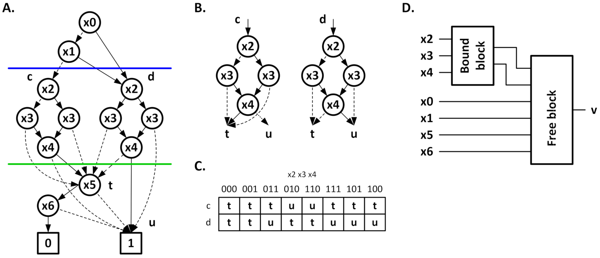
Consider the function described by BDD, as shown in Case A of
Figure 11. The introduced cutting lines divide the BDD into 3 sections. The slice containing the variables
x5 and
x6 is associated with the free set. A slice containing the variables
x2,
x3, and
x4 is associated with the bound set. On the other hand, the slice associated with the variables
x0 and
x1 can be associated with either the bound set or free set (in the present case, it was associated with the free set). When considering the slice between the cut lines (shown in
Figure 11B), it is crucial to determine the number of bound functions necessary to perform such decomposition. As can be seen in Case B of
Figure 11, this section is an SMTBDD diagram [
36,
37]. This slice has two roots (labeled c and d) and leaves symbolically labeled t and u. To determine the number of necessary bound functions, it is necessary to create a root table [
36,
38].
The root table, for the case in question, is presented in
Figure 11C. The lines of this table correspond to the individual root (c and d). On the other hand, the columns correspond to the possible combination of variables in the considered SMTBDD). The cells contain symbolic marks of leaves that are reached from the root (associated with the row), along the path determined by the combination of variables in a given column for the analyzed SMTBDD. Thus, patterns of the columns can be distinguished in the root table. Thus, the number of bound functions is the number of bits necessary to distinguish between different column patterns in the root table. For Case C, of
Figure 11, there are three column patterns, which leads to the need to use two bound functions. The obtained division is shown in Case D, of
Figure 11.
Simple serial decomposition is the basis for more complex decomposition models, such as multiple or iterative decomposition [
39]. Additionally, it should be remembered that the quality of the obtained solutions depends on the order of variables in the BDD [
40]. The key methods are to quickly estimate the effectiveness of mapping in blocks with specific configuration capabilities [
35,
39], as well as optimization methods, such as non-disjoint decomposition [
35].
In practice, the implementation of a single function is very rare. As a rule, multi-output functions are implemented in FPGAs. In this situation, a very effective approach is to share logic resources between structures associated with single functions. It turns out that this approach does not always lead to good results, and resource sharing should only be partial [
39]. Thus, a question arises on how to find the bound function common to several single functions, so that the obtained solutions are efficient, in terms of the use of logical resources [
39].
Consider the two logic functions, described by BDD (shown in Cases A and B, of
Figure 12). The decomposition was performed with the use of multiple cuts, which led to the formation of the root tables shown in Case C, of
Figure 12. There are four root patterns (A, B, C, and D) in the root table for the function
f0, which leads to the need to use two bound functions. However, in the root table for the
f1 function, there are also four column patterns (E, F, G, and H), which also leads to the need to use two bound functions. Thus, in an implementation without resource sharing, the total number of bound functions is four. Questions arise as to whether it is possible to find a bound function common to
f0 and
f1. To analyze this problem, a graph was created, in which the nodes correspond to the combination of variables from the columns of the root tables. Each node can be assigned a symbolic column pattern designation for both
f0 and
f1. By combining the nodes with the same symbols of the columns, we obtain the graph shown in Case D, of
Figure 12. It turns out that the graph has been divided into three parts. Thus, it is possible to distinguish individual parts by the value that the newly introduced function
g0′ will take, which will be shared for both
f0 and
f1. If the function
g0′ takes the value 0, nodes connected with red edges are indicated. Otherwise, the group containing the remaining nodes is indicated. Of course, it is necessary to introduce the two additional bound functions
g10 and
g11 separately for both functions
f0 and
f1. This approach has reduced the total number of bound functions from four to three.
The logic structure created after mapping the multi-output function
f0f1 in LUT_X blocks (where X is the number of block inputs) is shown in
Figure 13.
5. Hardware Mapping Method of a Partially-Mapped Flow Graph
Developed logic optimization of data flow graphs results in the mapping of a subgraph, representing the logic operations in look-up tables. This enables using a developed, BDD-based decomposition strategy to improve implementation. Before the hardware mapping is performed, the input data flow graph is subject to the accommodation of the nodes to available components. Nodes representing arithmetic operations must meet the mapping requirements implied of available arithmetic blocks in the library. Multiple argument nodes are expanded into two arguments nodes. To balance computation time, the expansion procedure calculates the computation time completion, using an as soon as possible approach for each argument node. The computation time-driven expansion method selects arguments with the earliest computation completion time to be expanded to the two-argument node. This approach enables the expanding a node in a processing time balanced manner that differs from typical balanced tree expansion (balancing number of nodes for left and right branches). The arithmetic complement edge attribute is translated into an equivalent structure in 2′s complement system, using logic inversion and the addition of 1. After completing all mentioned operations, the data flow graph is ready for hardware mapping.
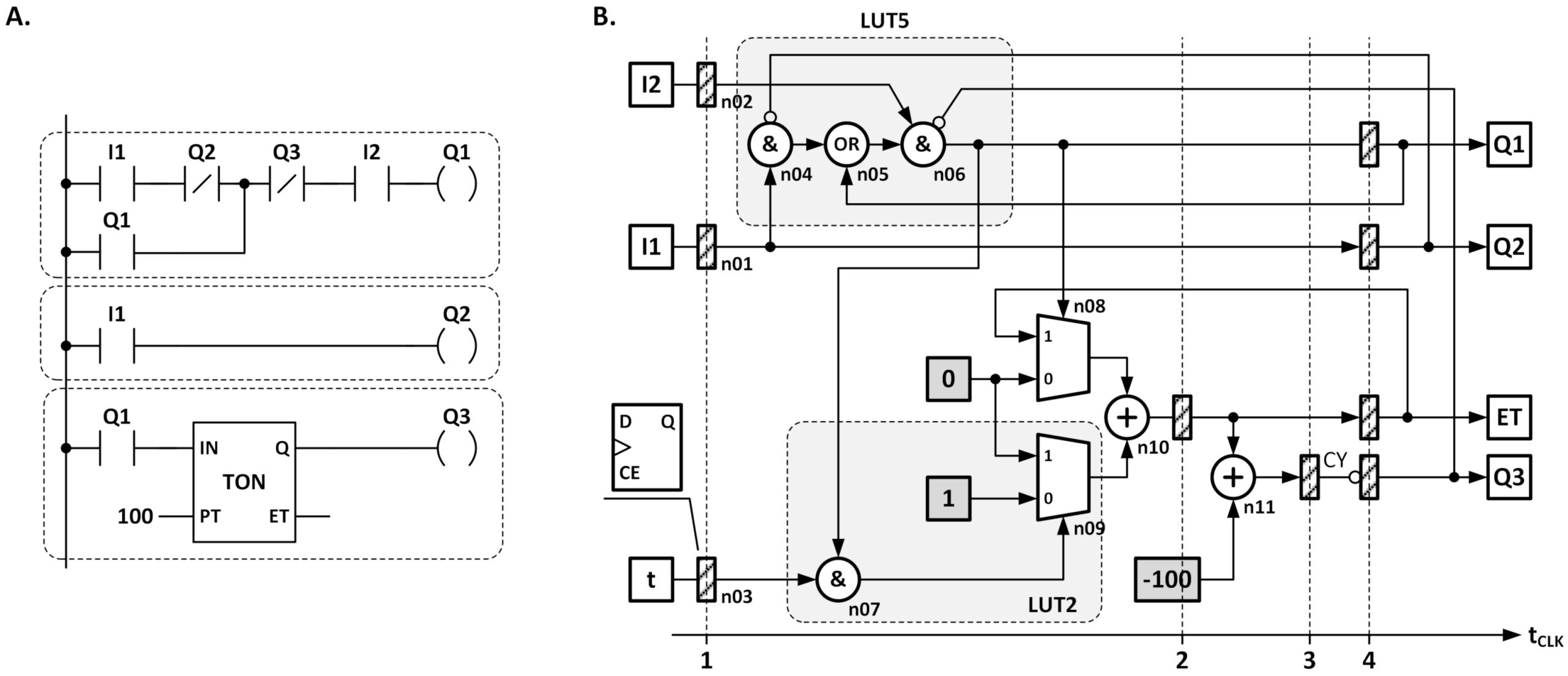
An exemplary LD program is shown in
Figure 14 (Case A). To illustrate the extended ability of the proposed mapping strategy, the program utilizes the TON timer, which uses arithmetic and logic operations. Next, the program is translated into a data flow graph. Case B shows a data flow graph after the initial optimizations and scheduling of operations. Arithmetic operations, due to different complexities and numbers of cycles for completing the computations, require the use of a scheduling process. Additionally, it should be noted that multiplication and division can be implemented using combinational or sequential approaches. To reduce resource requirements, the sequential approach is used in the direct implementation. The direct implementation utilizes an as soon as possible (ASAP) scheduling approach [
22,
41]. This method enables obtaining the resource allocation, with the smallest number of clock cycles to complete computations. In the block diagram, there are marked nodes selected for the LUT mapping procedure. At the bottom of the data flow graph, a timeline is shown, scaled in clock cycles. The hatched rectangles denote registers placed across the structure. The controller is equipped with a set of input registers (updated in the first calculation cycle) and a set of output registers (updated in the last calculation cycle). All inputs are sampled simultaneously at the beginning of the calculations and all outputs are updated in the last computation cycle. The arithmetic components are passed to the implementation tools as library components. The conditional choice nodes (multiplexers) are a subject of expansion to logic implementations, when nodes connected to selection inputs represent constants or logic operations. In the considered data flow graph nodes, n07 and n09 are translated into the logic structure, while meeting the given requirements.
The data flow graph is used for preparing the synthesizable description for the FPGA implementation tools. In the experiments, Xilinx FPGAs families are used [
42]. In
Figure 15, the register transfer level block diagram is shown, obtained after mapping the data flow graph to the respective hardware components. The subgraphs defining logic operations have been substituted, with direct mapping to LUT components.
The multiplexer selecting among constants 0 and 1 is substituted by a logic circuit. It should be noted that multiplexers selecting among constant values are always expandable to logic operations. Each bit of the results belongs to the set:
, where
f is a selection function of the multiplexer. The other optimization, after translating a multiplexer, is connected with adder optimization. FPGA devices implement additional circuitry, enabling the simplified implementation of ripple carry adders using carry chain [
28]. In LUT6 based architectures (since Virtex 5), the carry chain links four LUTs, located in a slice, together. To improve the performance of the adder, the 4-bit carry chain utilizes look-ahead adder optimization and dedicated connection resources with low delay and direct connection to vertically adjacent slices (creating vertical carry lines, implemented using metal segments). Finally, the hardware structure is supplemented with the cycle controller that manages the data flow among registers, according to the given schedule. The controller is implemented using a shift register that simplifies the implementation of rotating one pattern dependent on the RUN signal, as shown in the waveform in
Figure 15.
6. Experiments
To illustrate the performance of the direct implemented controllers and support of hardware mapping strategy for logic operations, a set of control circuits was implemented. The resulting comparison was partitioned into the comparison of the logic block utilization for the part of the controller responsible for logic operations, complete implementation, and final controller performance. The Artix 7 FPGAs from Xilinx [
28,
42] were selected for experiments.. The comparison was made between the dekBDD, the academic ABC system, and commercial tools. In the case of the ABC system, they used the following synthesis script: “strash; dch; resyn2; if -K 5 –p”. This complex command line assures mapping in LUT blocks with 5 inputs, using resynthesis. The experimental results, accomplished by the authors, have proved that the obtained results are very efficient, in terms of used resources and power consumption.
The results are gathered in
Table 1. To perform the benchmark, a two-state processing part, that is extracted for implementation using the dekBDD toolset, has been redirected to other tools, too. Benchmark programs AGV, GRAVEL, and MIX_BRIX are examples of the IEC61131-3 standard [
11]. Those benchmarks illustrate the ability to create an implementation from a description using SFC and LD languages. There are also defined mathematical dependencies that compare the weight of the delivered materials or count the number of items delivered to the controlled process (MIX_BRIX, GRAVEL). The AGV controller is the simplest one, utilizing only logic dependencies. The SFC hardware implementation consists of multiple two-state finite state machines. Each machine is associated with the respective step. This implementation perfectly fits the FPGA device architecture, which offers a large number of flip-flops. Its number is twice the LUT6 number, in the case of the Artix family. It should be noted that LUT6 can operate as two independent LUT5 blocks, fed with the same set of signals offering the architecture 2 × LUT5. The method of implementing SFC resembles the method of one-hot encoding. This results in simplified implementation, while immediate decoding of the condition is possible by analyzing the active steps. This also proves the feasibility of the mapping model of SFC for the FPGA architecture. Summarizing benchmarks AGV, GRAVEL, and MIX_BRIX proved the efficiency of SFC mapping. The excitation functions of the steps do not require specific decomposition and are implemented successfully with the same number of resources by all evaluated tools.
The LIFT_n is a scalable implementation of a lift controller in an n-storied building using LD-only implementations. The controller brings the complex logic dependencies of controlling lift cabin movement (up or down) and processing the requests. The number of handled floors increases the logic condition complexity. There are gathered numbers of inputs and outputs of logic structure for respective implementation. This set of benchmarks shows the efficiency of decomposition models. It could be observed that the dekBDD offers results comparable to Synplify and Vivado (LIFT_12 slightly outperforms Synplify, by about 4%). To summarize, the proposed decomposition offers a better result, in comparison to the ABC system.
In
Table 2, complete hardware requirements for the entire controller, including arithmetic computations, are gathered (timers, counters, comparators, etc.). The number of flip-flops is shown (FF column). The number of clock cycles, required for completing the calculations, is shown in the T
CK column. Next, the computation performance is shown. The f
MAX column gathers the maximal clock frequency. Using the maximal frequency and required number of clock cycles, the computation time is calculated (column t
CALC). The time given in this column covers complete computation time. Finally, a performance comparison is made to logic controllers, based on instruction execution. The I
CNT column gathers the number of instructions a particular program consists of. For the simplicity of the calculations, it is assumed that each instruction can be executed in a single cycle (this assumption gives the handicap to PLC CPU). The THP column contains the throughput of the controller structure, expressing performance in billions of instructions executed per second.
The proposed direct hardware implementation of the controllers offers extraordinary computation performance. It should be noted that, opposite to programmatic implementation, there is a constant computation time, independent from the logic conditions of program execution. The number of clock cycles is relatively low. The GRAVEL program requires seven clock cycles to complete computation, due to mutually dependent arithmetic operations. It should be noted that the mapping strategy that allocates arithmetic blocks in separate cycles, as required for computation completion, allows for achieving the maximal clock frequency (above 300 MHz).
An interesting observation can be made, in the case of the LIFT_n controller implementation. The controller requires four clock cycles to complete the computation. The growing complexity of the controller (4, 8, and 12) increases the propagation delay, reducing the maximal clock frequency (from 307.0 MHz to 242.8 MHz). It should be noted that the increase in complexity results in increased throughput. This shows a unique property of direct hardware implementation that offers extraordinary computation performance, using massively parallel computations. It should be noted that, in all cases, the maximal clock frequency that can be applied to the FPGA device is significantly greater than 200 MHz. In practical applications, assuming a constant clock frequency of 200 MHz for the controller, the response time is between 10 ns for AGV to 35 ns for GRAVEL (for the considered benchmarks).
The comparison with other implementation methods is gathered in
Table 3, including program execution times for Simatic S7-319 [
43] and LD direct hardware implementation methods. The LD direct implementation methods were divided into the rung-based method (RG column) [
8,
10] and the rung-based method with optimization [
9,
12,
13,
21] (RGO column). The last column (DFG column) holds the results for the developed method. The test programs AGV, GRAVEL, and MIX_BRIX are described using SFC. To be able to synthesize those programs, they were translated to the equivalent LD. The Simatic S7-319 execution time is calculated for the shortest instruction execution time. For all direct hardware-implemented controllers, the clock signal frequency is assumed to 200 MHz (1 T
CK = 5 ns). The LD implementation, presented in [
9,
12,
13,
21], does not enable the implementation of timers, counters, and functional blocks. Results presented here are based on the experience and estimation of implementing the timer and arithmetic modules (performed by the authors). To summarize, the presented DFG assures an extended synthesis of the control program that offers the best performance. The rung-based method (RG column) offers a performance improvement, in comparison to PLC implementation. Further performance improvement is observed in the rung-based optimized method (column RGO). For the RG and RGO methods, performance is dependent on the program representation using a ladder diagram. Two functionally equivalent programs can be drawn using the different number of rungs that directly affect the RG method. Switches and coils order the results with the different numbers of cycles required to complete computations. This is a result of examining variable dependencies only. The proposed DFG method offers the shortest execution time and is capable of the direct implementation of programs using both LD and SFC languages. The statement analysis and translation to intermediate form makes the implementation process independent from the LD program drawing.


