Article

Nanoelectrode Ensembles Consisting of Carbon Nanotubes

Department of Chemistry, University of Cincinnati, Cincinnati, OH 45221-0172, USA
*
Author to whom correspondence should be addressed.
Appl. Sci. 2021, 11(18), 8399; https://doi.org/10.3390/app11188399
Submission received: 13 August 2021 / Revised: 3 September 2021 / Accepted: 7 September 2021 / Published: 10 September 2021
(This article belongs to the Special Issue Nanoelectrochemistry for Single Particle Detection)

Abstract

:
Incorporating the nanoscale properties of carbon nanotubes (CNTs) and their assemblies into macroscopic materials is at the forefront of scientific innovation. The electrical conductivity, chemical inertness, and large aspect ratios of these cylindrical structures make them ideal electrode materials for electrochemical studies. The ability to assemble CNTs into nano-, micro-, and macroscale materials broadens their field of applications. Here, we report the fabrication of random arrays of CNT cross-sections and their performance as nanoelectrode ensembles (NEEs). Single ribbons of drawable CNTs were employed to create the CNT-NEEs that allows easier fabrication of nanoscale electrodes for general electrochemical applications. Surface analysis of the prepared NEEs using scanning electron microscopy showed a random distribution of CNTs within the encapsulating polymer. Electrochemical testing via cyclic voltammetry and scanning electrochemical cell microscopy revealed voltametric differences from the typical macroelectrode response with the steady-state nature of NEEs. Finally, when the NEE was employed for Pb2+ detection using square-wave anodic stripping voltammetry, a limit of detection of 0.57 ppb with a linear range of 10–35 ppb was achieved.

1. Introduction

Nanoelectrodes have many characteristics that are important for analytical and physiological applications, including a low charging current [1,2], enhanced mass transport [1,2,3,4,5,6,7,8], and the ability to perform in more resistive media [2,3,9,10]. However, working with an individual nanoelectrode can be difficult because the small size complicates fabrication, and the low current response requires more sensitive instrumentation. To overcome the low current response of an individual nanoelectrode, nanoelectrode arrays (NEAs) or ensembles (NEEs) have been fabricated [2]. Although the literature makes little distinction between these terms, NEAs tend to consist of nanoelectrodes with controlled interspacing, typically equidistant, whereas NEEs have randomly arranged nanoelectrodes [11]. In both cases, the nanoelectrodes work in parallel, which significantly improves the signal-to-noise ratio [3,5,8,9].
NEAs and NEEs can be fabricated from various materials such as gold [10,12,13,14,15,16,17,18,19], platinum [16], TiO2 [20,21], ZnO [22,23], CeO2 [24], nickel [25], boron-doped diamond [26], carbon fibers [27,28], SiO2 with a Ti/Pt coating [29], and carbon nanotubes (CNTs). NEAs and NEEs are typically fabricated using one of two methods. The first method is a template synthesis approach, which involves either electroless or electrical deposition of a metal into a porous template [10,30]. Common template membranes include anodic aluminum oxide [16,20] and porous polycarbonate [10,12,13,17,18,19,21,25]. The second method uses self-assembled monolayers to fabricate NEAs and NEEs [30].
NEAs and NEEs have been applied as biosensors [16,22,24,27], dopamine sensors [14,15,23,26], immunosensors [12,13,19], and glucose sensors [17,31], as well as for intercellular electrophysiological imaging [29,32]. A crucial factor in the increased sensitivity of NEAs and NEEs as sensors is analyte diffusion to the electrode surface. Because the sensing areas of NEAs and NEEs are on the nanoscale, the diffusion layer thickness is comparable to that of the electric double layer, which leads to an increase in the mass transport of molecules to the electrode surface [33]. In cyclic voltammetry (CV) tests with NEAs or NEEs, a redox-active analyte either rapidly establishes a steady-state diffusion profile or exhibits a time-dependent diffusion-limited response. When the spacing between the nanoelectrodes within an array is 12.5 times greater than the nanoelectrode radius, the diffusion profiles of the nanoelectrodes do not overlap. The resulting convergent flux of dissolved redox species leads to a sigmoidal voltammogram, indicating a steady-state response [33]. When the spacing between the nanoelectrodes is less than 10 times the nanoelectrode radius, the radial diffusion to neighboring nanoelectrodes overlaps, leading to a diffusion-controlled CV response for reversible redox analytes. Even with such overlap, NEAs and NEEs can provide greater sensitivity than macroelectrodes [33]. Because an NEE has a smaller electroactive area than a planar electrode, the charging current is lower, which is an important factor for achieving enhanced faradaic signals [3,4,8].
As cylindrical macromolecules with nanoscale diameters, CNTs are an ideal material for fabricating NEAs and NEEs, where dimensions of 1–100 nm are required [2]. NEAs and NEEs typically employ vertically aligned CNTs (VA-CNTs) that are grown through chemical vapor deposition (CVD). CNTs have been reported to exhibit excellent performance as electrodes due to their wide working potential range [5,6,34], chemical inertness [5,9,35], good electrical conductivity [3,5,9,35,36,37], high surface area [9], functionalization ability [5], electrocatalytic properties [8,9,38], and biocompatibility [6,9,34,37]. CNTs also show fast electron transfer characteristics [6,8,9]. Electron transfer by CNTs has been studied at both their open ends and sidewalls, with faster electron transfer observed at the open ends [5,34]. During growth, VA-CNTs can be encased in a passivation layer (e.g., silicon dioxide or epoxy) to cover the sidewalls and restrict chemistry to the open ends. As the density of CNTs within an array can be controlled during the synthesis process, it is possible to achieve a wide range of CNT-NEAs that exhibit different electrochemical responses, with high-density arrays behaving as macroelectrodes, and low-density arrays showing steady-state responses. However, current fabrication methods for CNT-NEAs, especially low-density CNT-NEAs, require catalyst patterning techniques and instrumentation that are expensive and not readily available. There are also difficulties associated with encapsulating CNT arrays in a passivation layer [28]. Despite these fabrication difficulties, VA-CNT arrays have been used to create NEAs and NEEs for glucose biosensors [8], heavy metal detection [4,5], dopamine detection [6,37], and DNA/RNA sensors [34,39,40,41,42,43]. The use of drawable (also called spinnable) CNTs provides a simpler bottom-up assembly method that can be used to fabricate nano-, micro-, or macroelectrodes [37,44]. Lin et al. employed spinnable CNTs to fabricate band electrodes, which are macro-sized in length but sub-micron sized in width, allowing for high mass transfer coefficients and response currents [37]. Our team has fabricated microelectrodes of different diameters below 100 micron from spinnable CNTs that have shown excellent performance when employed as sensors [44].
There are many advantages of using NEAs and NEEs in research. Their low charging current, enhanced mass transport, and ability to be used in resistive mediums has attracted many electrochemical sensor developers. Most CNT-NEAs and NEEs fabrication methods reported have employed expensive fabrication methods to synthesize well-spaced CNTs and encapsulate them with a passivation layer that also has drawbacks. This work reports a simpler method for fabricating CNT-NEEs that employs drawable or spinnable multiwalled CNTs. Rather than controlling the catalyst amount and position when growing the CNTs, aligned CNTs were easily drawn out into a CNT film/ribbon, and a passivation polymer layer of hydrogenated nitrile butadiene rubber (HNBR) was employed to separate each CNT layer. The electrochemistry of these CNT-NEEs was investigated using CV and scanning electrochemical cell microscopy (SECCM) to demonstrate their steady-state nature. Finally, the CNT-NEEs were employed to detect toxic Pb2+ in acetate buffer.

2. Materials and Methods

2.1. Chemicals and Instrumentation

Drawable CNT arrays were synthesized using CVD with ethylene from Wright Brothers (Cincinnati, OH, USA) as the carbon source and argon as the carrier gas. Physical-vapor-deposited Fe/Co was employed as the catalyst from GoodFellow Corporation (Coraopolis, PA, USA). The synthesis details have been reported by our team elsewhere [45,46]. Zetpol 1020 HNBR from Zeon Chemicals L.P. (Louisville, KY, USA) was used in the fabrication of CNT-NEEs. The CNT-NEEs were cleaned using a Plasma Prep III solid-state air plasma cleaner from SPI Supplies (West Chester, PA, USA). The CNT-NEEs were assembled using quick dry epoxy resin (J-B Weld), fast dry silver paint (Ted Pella, Redding, CA, USA), and a copper wire. Electrochemical measurements used hexamineruthenium(III) chloride (Ru(NH3)6Cl3 or Ruhex, 98%) from Acros Organics (Waltham, MA, USA) and potassium chloride (KCl, 99%) from Sigma-Aldrich (St. Louis, MO, USA) prepared in Milli-Q ultrapure water (18.2 MΩ cm). Lead detection was performed using sodium acetate trihydrate (BioXtra, 99.0%) from Sigma-Aldrich, glacial acetic acid (Pharmco, Shelbyville, KY, USA), and a lead standard for ICP (Sigma-Aldrich), which were prepared in Milli-Q ultrapure water (18.2 MΩ cm). Optical microscope images of the electrodes were obtained using a Keyence digital microscope (Osaka, Japan). Electrochemical testing was performed using a CH Instruments electrochemical workstation (CHI760E) (Austin, TX, USA) and a BASi Epsilon EClipse potentiostat/galvanostat (West Lafayette, IN, USA). Scanning electron micrographs were obtained on a Philips FEI XL30 ESEM (North Billerica, MA, USA).

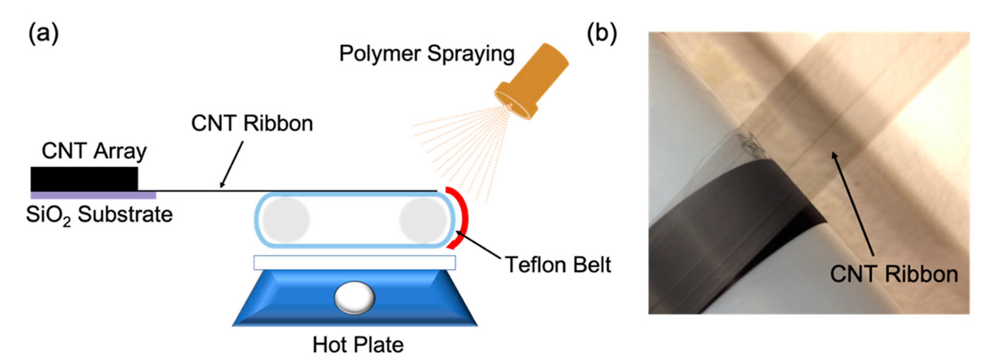
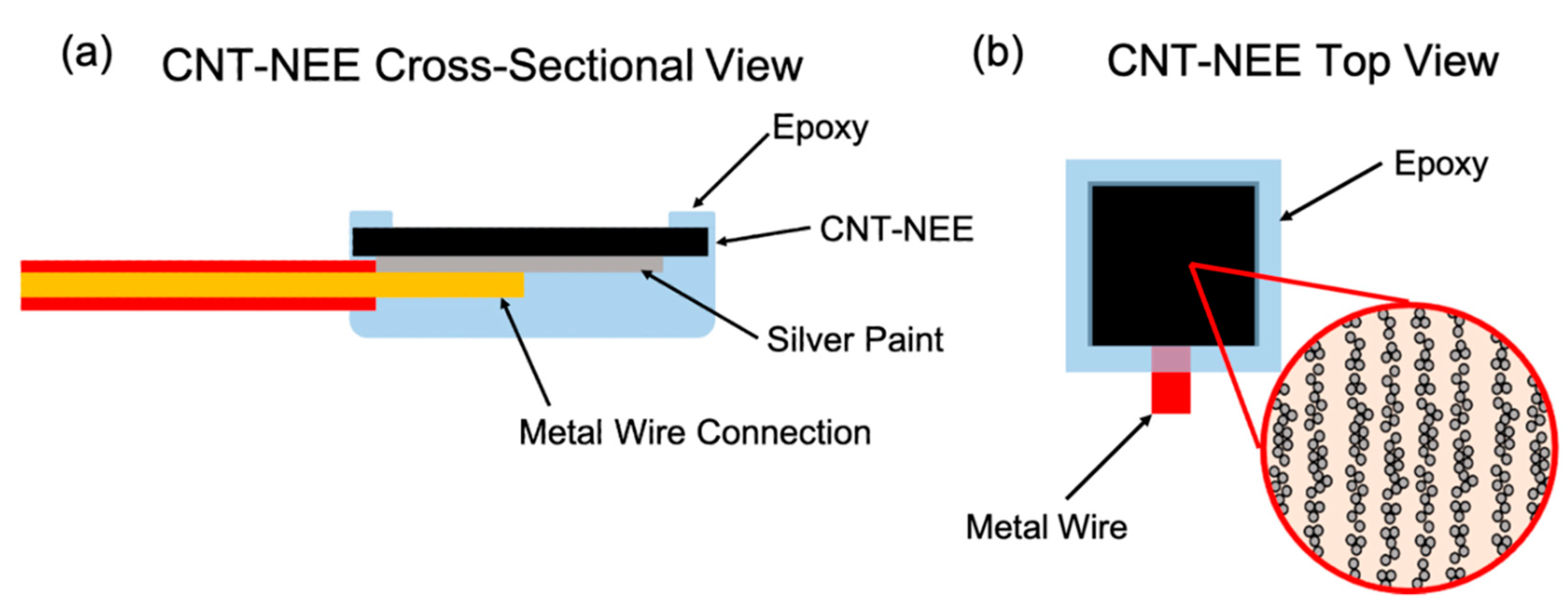
2.2. CNT-NEE Fabrication

CNT-NEEs were fabricated by alternating layers of HNBR with ribbons of spinnable CNTs, as shown in Figure 1. The spinnable or drawable CNTs were grown in a vertically aligned forest, typically with heights of ~450 µm [45,47], and then drawn into ribbon-like films (Figure 1b). The CNT films were relatively dense (Figure 2a) but contained separated CNTs and bundles (Figure 2b). HNBR was chosen as the encapsulating polymer due to its strong interaction with CNTs, as previously reported by Alvarez et al. [48]. Initially, a layer of HNBR dissolved in acetone was sprayed on the Teflon belt, which moved continuously on a motorized drum. The bottom side of the Teflon belt was positioned 10 mm away from a hot plate, allowing acetone to evaporate and HNBR to dry before collecting the CNT film. The spinnable CNTs were pulled out as a thin film onto the HNBR layer, and more HNBR was then sprayed over the CNT film, encapsulating the CNTs. To build up multiple layers (hundreds), the HNBR layer was allowed to dry before adding another layer of CNTs. The layers on the belt were cut and stacked to create a bulk material of aligned CNTs within HNBR, which was then cured under heat (160 °C) and pressure (4000 PSI). Using a cryomicrotome, the HNBR-encapsulated CNTs were sectioned orthogonal to the direction of the CNTs with ~100 μm thickness, in a similar manner to our prior work [44]. The resulting CNT-NEE had exposed open ends that were employed as nanoelectrodes.
An electrical connection to the CNT-NEE was established by attaching a copper wire to the backside of the CNT-HNBR material using fast drying silver paint. Subsequently, an epoxy resin was placed over the copper wire and silver paint and around the edges of the CNT-HNBR material, which, after drying, acted as a dielectric protection layer. An illustration of the CNT-NEE assembly is shown in Figure 3a, and Figure 3b illustrates the nature of the nanoelectrodes at higher magnification.

2.3. SECCM Measurements

Nanopipettes were fabricated from single-barreled quartz capillaries (1 mm OD, 0.7 mm ID, Q100-70-10, Sutter Instrument (Novato, CA, USA), using a P2000 laser puller (Sutter Instrument, Novato, CA, USA). Electrochemical characterization was performed by filling the nanopipettes with 0.1 M KCl solution and measuring the resistance at the nanopipette opening using CV. Based on the measured resistance, the average nanopipette diameter was determined to be ~240 nm. Subsequently, the nanopipette was filled with 5 mM Ruhex in 50 mM KCl solution, which formed a nanodroplet-sized meniscus at the tip. To create an electrical connection, an Ag wire (99.9%) was polished and bleached to create Ag/AgCl and then inserted into the filled nanopipette. The nanopipette was attached to a piezoelectric positioner (P621-ZCD, Physik Instrumente, Auburn, MA, USA). The prepared CNT-NEE sample was mounted on an xy piezoelectric positioner (MCLS03792, Mad City Labs, Madison, WI, USA). The nanopipette was positioned over the CNT sample with the aid of stepper motors (MPC-200, Sutter Instrument, Novato, CA, USA) and an optical camera. Cyclic voltammograms were obtained using Chem-Clamp (CHEM N = 1, Dagan Corporation, Minneapolis, MN, USA) coupled with Warwick Electrochemical Scanning Probe Microscopy Software. The experiments were carried out in a home-built Faraday cage.

3. Results and Discussion

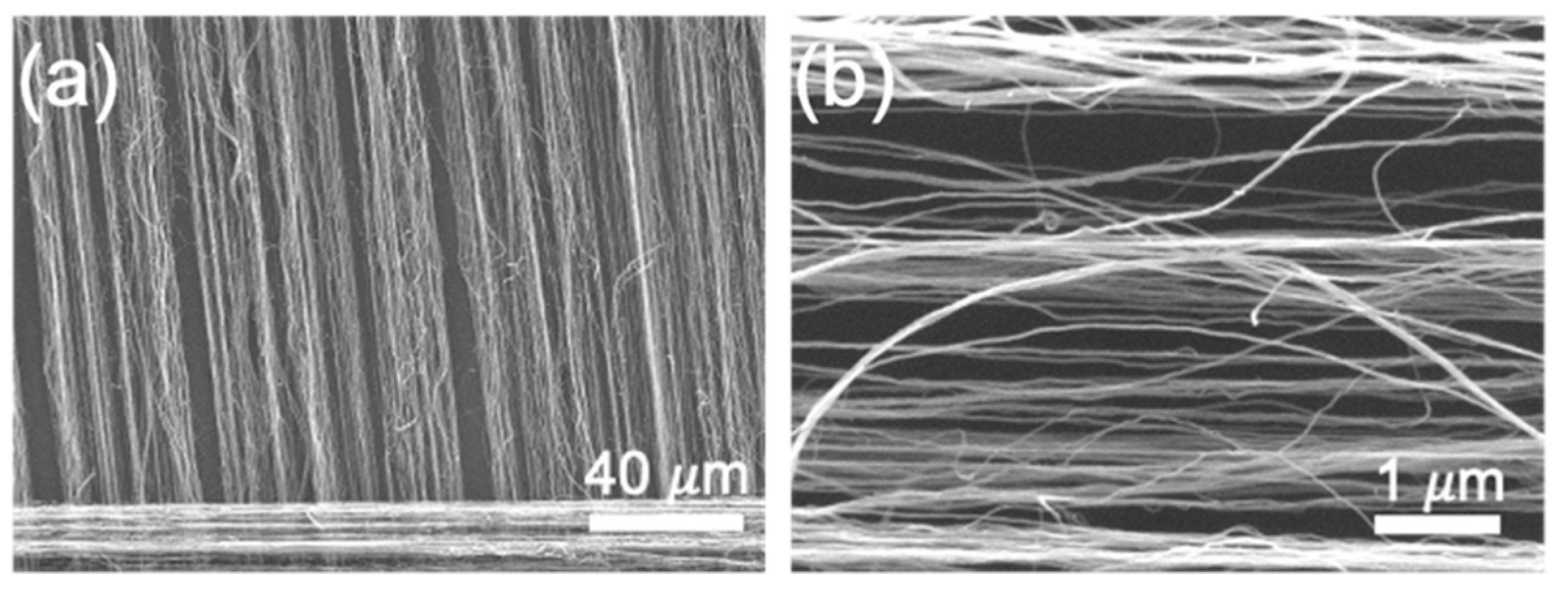
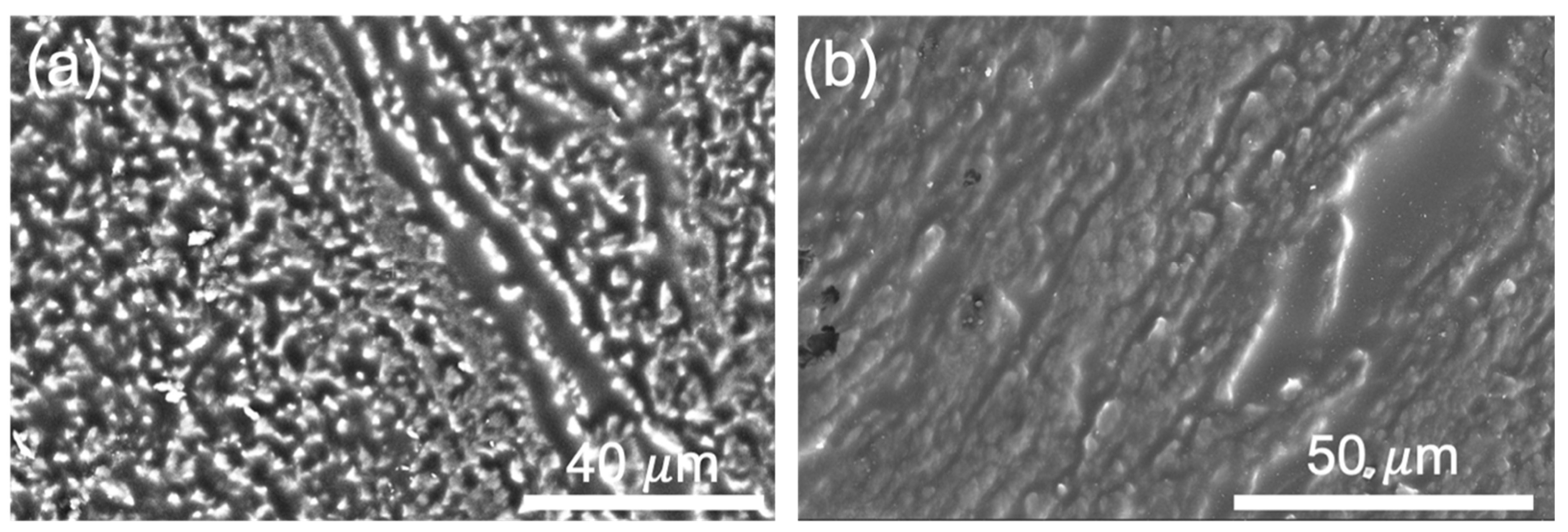
3.1. CNT-NEE Surface Analysis

Figure 4 shows scanning electron microscopy (SEM) images of the CNT-NEE cross section after cryomicrotoming, where the brighter spots in Figure 4a correspond to the CNT open ends. The SEM images reveal that HNBR completely encapsulated the CNTs, leaving no void spaces between the polymer and the CNTs. The CNT-NEE sample in Figure 4b was treated for 60 s using an air plasma cleaner, which etched the polymer layer, thus cleaning the surface and exposing more CNTs. A visual comparison of the SEM images in Figure 4a,b shows that the plasma-cleaned CNT-NEE contained more CNTs, but greater lengths of the CNTs were exposed. To limit the CNT sidewalls exposed, the plasma cleaning time was decreased to 15 s for the CNT-NEE electrodes employed in this work. Although this fabrication method does not allow the precise positioning of CNTs and bundles, the spacing among the nanoelectrodes should be statistically similar because it is related to the CNT density in the drawn ribbon. As shown by the high-magnification SEM image in Figure 2b, the ribbon-like CNTs were extremely porous. Although the CNTs form small bundles of multiple CNTs, no bundle should be larger than 50 nm in one direction, as determined by the previously nature of the drawable CNTs. This thickness of the individual film was reported by our team elsewhere [49]. The observed porosity of the CNT film is important for the fabrication of CNT-NEEs, because it provides separation between random nanoscale bundles and individual tubes.
Using high-magnification SEM images and ImageJ software, the approximate percentage areas occupied by CNTs and HNBR within the CNT-NEE were estimated (Supplementary Materials Figure S1; for details, please see the supporting information). The CNT-NEE was found to contain approximately 22.16% CNTs. Although this approach may only provide an estimate of the maximum area, it can act as a guide for future comparisons with electroactive areas determined using electrochemical methods. The obtained areal coverage may also be affected by the employed method, as SEM images are subject to distortion due to the brightness of CNTs and lack resolution for accurate assessments.

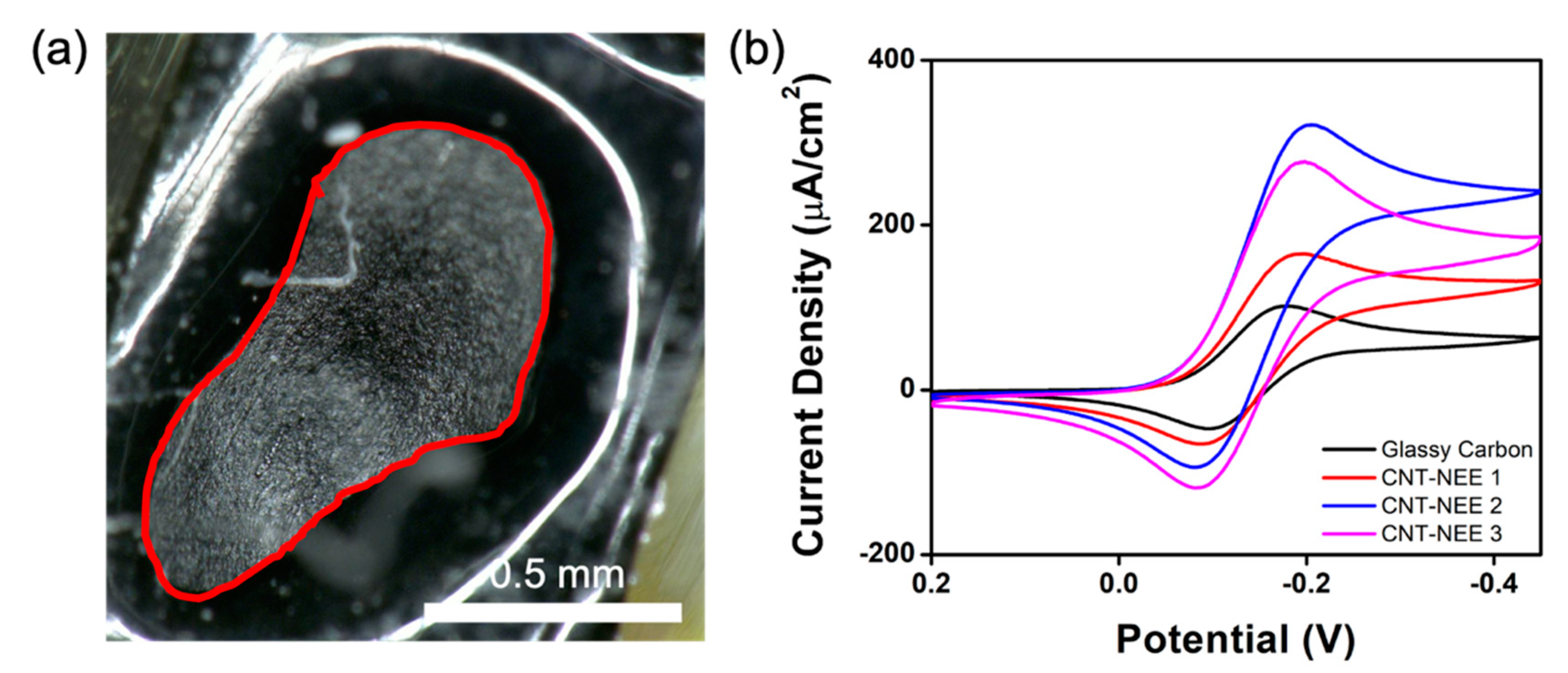
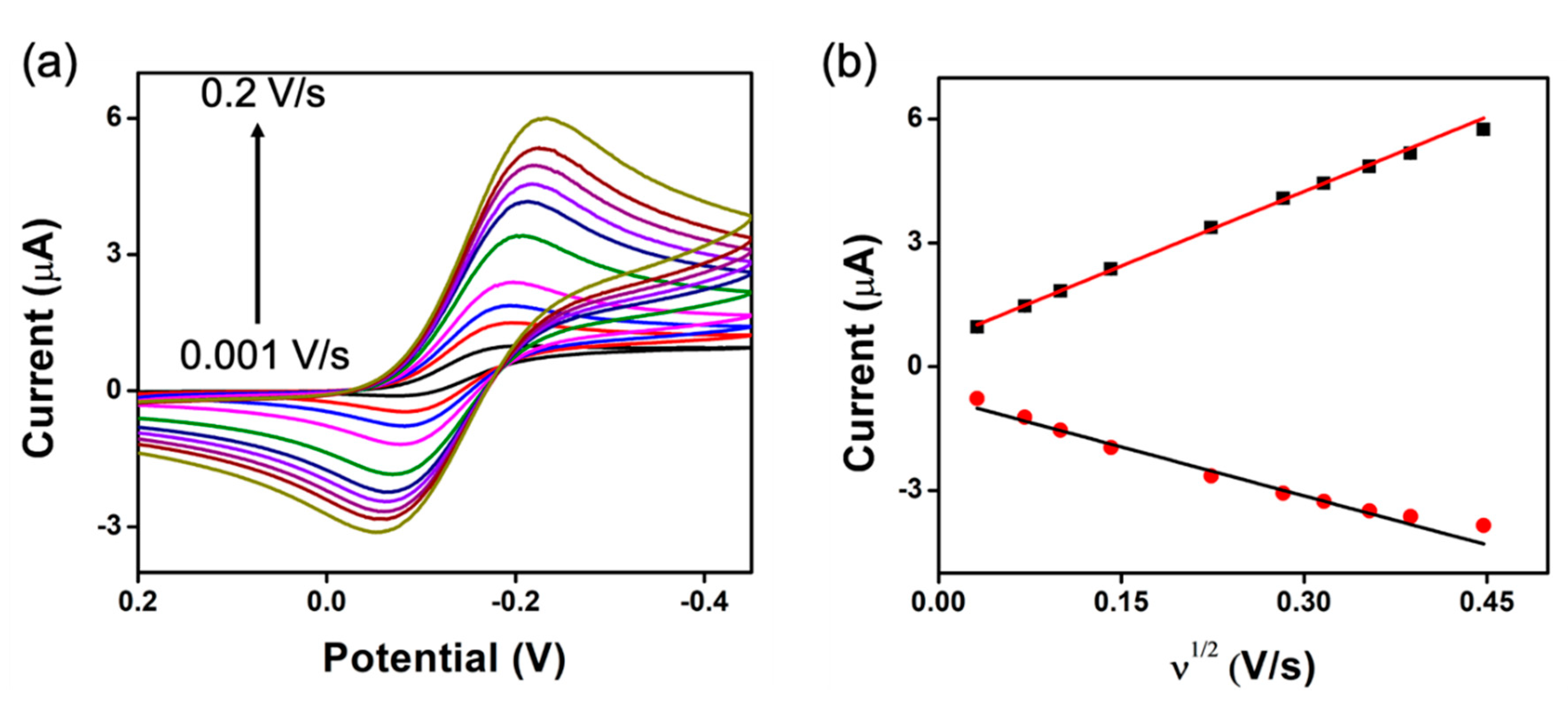
3.2. CV Characterization of CNT-NEEs

Using optical microscope images and ImageJ software, the geometrical surface area of the CNT-NEE was determined. Figure 5a shows the CNT-NEE surface, where the area outlined in red corresponds to the geometrical area of the CNT-NEE (Table 1) and the shiny region outside the red line corresponds to the dielectric epoxy that covered the edges to prevent electrolyte leaching into the metal connection sites. It is important to note that the area exposed to solution (named as the geometrical area) varied between CNT-NEE samples, as shown in Figure S2 and Table 1. The CNT-NEEs were initially tested using CV in the potential window of +0.2 V to −0.45 V at a scan rate of 0.01 V/s. A solution of 50 mM KCl was used as a blank to ensure the electrical connection was sufficient and that no contamination peaks were present.
Using a solution of 2.5 mM Ruhex in 25 mM KCl, the redox activities of the electrodes were investigated. The CV results for three CNT-NEEs (CNT-NEE 1, CNT-NEE 2, and CNT-NEE 3) and a traditional glassy carbon (GC) electrode are shown in Figure 5b. Owing to the differences in electrode areas, comparisons were made using the current densities, as determined by dividing the current response of each electrode by the corresponding active area (Table 1). The active areas of the electrodes were determined by capacitance measurements, as follows. In a solution of 0.1 M acetate buffer (pH 4.5), the CV response was recorded in the potential window of +0.2 V to +0.1 V at a scan rate of 0.2 V/s. From the CV response, the charging current was determined, which was then used to calculate the active area. First, the double layer capacitance was calculated using Equation (1).
i c = ν C d l
where i c is the charging current (A), ν is the scan rate (V/s), and C d l is the double layer capacitance (F). Subsequently, C d l was employed to determine the active area of each electrode using Equation (2).
C d l = ε 0 ε r A d
where ε 0 is the permittivity of free space (8.854 × 10⁻¹² F/m), ε r is the dielectric permittivity of the solution (6.15), A is the active area of the electrode (m2), and d is the diffusion layer thickness (m). As summarized in Table 1, the active areas of the CNT-NEEs were smaller than the geometrical areas, indicating that only a small percentage of the CNT-NEE geometrical area was occupied by CNTs while the remainder was occupied by HNBR. This finding is consistent with the SEM images and the estimation of the area occupied by CNTs (Figure S1).
A comparison of the normalized current responses revealed higher current densities for the CNT-NEEs than for the GC electrode. Thus, although the electrodes in the CNT-NEE were smaller than the traditional GC electrode, they showed larger current densities. To compare the charging currents of the GC electrode and the CNT-NEEs, a similar approach was used to convert the current response in a blank solution of 50 mM KCl to current density (Figure S3). The electrodes in the CNT-NEEs displayed a lower charging current than the GC electrode, which is promising in terms of the sensitivity of the CNT-NEEs for electrochemical applications, as demonstrated by the low signal-to-noise ratio for the detection of Pb2+ (see below).
The cyclic voltammogram of each CNT-NEE showed diffusion-controlled reduction and oxidation peaks for Ru(NH3)63+/2+ instead of a steady-state response, indicating that the electrodes in the CNT-NEE behaved as a macroelectrode. This macroelectrode response indicates that the CNTs within the CNT-NEE acted as a bulk material rather than as an NEA. It was hypothesized that for NEEs with bundles of CNTs as the sensing area, the CNT bundles would fall within the microelectrode range and thus exhibit a steady-state current response if each bundle experienced a radially convergent flux. The high density of CNTs and random distribution of CNTs with in the CNT-NEE material means the distance between the various sensing areas may not be significantly larger (12 times the radius) than the diffusion layer thickness resulting in the radial diffusion to all the CNTs to overlap, leading to planar diffusion to the electrode. These overlapping diffusion layers were also observed by Lin et al. and Koehne et al. [6,40] for CNT-NEAs with a high density of CNTs; however, the fabrication process for these CNT-NEAs requires encapsulating VA-CNT arrays. The CNT-NEEs in this work used a simpler fabrication process, which also created a large amount of bulk material, allowing for many electrodes to be fabricated. The CNT-NEEs reported here were fabricated using drawable CNTs with an average diameter of 8 nm, and the extremely porous CNT ribbon (Figure 2b) was expected to have large spacings within the constituent CNT bundles. As the CNT-NEEs exhibited macroelectrode CV responses, it was concluded that the spacing between the nanoelectrodes was not much greater than the diffusion layer thickness. The diffusion layer thickness was estimated from the CV response using Equation (3).
δ = π D R T F ν
where δ is the diffusion layer thickness, D is the diffusion coefficient (8.2 × 10⁻⁶ cm2/s), R is the gas constant (8.31 J/mol·K), T is the temperature (298 K), F is the Faraday constant, and ν is the scan rate (0.01 V/s). The estimated diffusion layer thickness of δ = 81.3 µm was significantly larger than the estimated distance of tens of nanometers between the CNT nanoelectrodes within the CNT-NEE. This finding again indicates that the diffusion layers of the individual sensing areas overlapped, resulting in a planar diffusion response at the electrodes in the CNT-NEE.
The peak-to-peak separations ( Δ Ep) calculated for the three CNT-NEE samples (107 mV, 124 mV, and 115 mV) were much greater than the reversible peak separation of 59 mV based on the Nernst equation. A similar quasi-reversible electrochemical reaction on CNT electrodes was reported by Koehne et al. [40]. The quasi-reversible nature of the CNT-NEEs was further supported by the observation that the cathodic peak currents were higher than the anodic peak currents at various scan rates (Figure 6a) [40,41,43]. Both peak currents were plotted against the square root of the scan rate ( ν 1 / 2 ) (Figure 6b) and against the scan rate (Figure S4). Linear relationships were observed for the cathodic and anodic peak currents with   ν 1 / 2 , as represented by Equations (4) and (5), respectively, indicating that the electron transfer process was diffusion controlled.
i p c   ( μ A ) = ( 12.05 ± 0.12 ) υ 1 2   ( V / s ) + ( 0.63 ± 0.04 )
R2 = 0.999
i p a   ( μ A ) = ( 7.91 ± 0.31 ) υ 1 2   ( V / s ) ( 0.76 ± 0.05 )
R2 = 0.987
However, because of the quasi-reversible nature of the CNT-NEE, the anodic peak currents were lower than the cathodic peak currents, and the linearity of the relationship was decreased, likely by the adsorption of reduced analyte species. The diffusion of reduced electroactive species from the electrode surface during reduction can result in the presence of a lower concentration of product during oxidation [50].
Owing to the proximity of the CNTs in the NEE, the diffusion layers overlapped, resulting in planar diffusion and a bulk electrode response. However, the CNT-NEE is made up of many nanoscale CNTs, which should individually behave as nanoelectrodes. To investigate the possibility of a steady-state response for the CNT-NEEs, CV characterization was conducted using the SECCM technique.

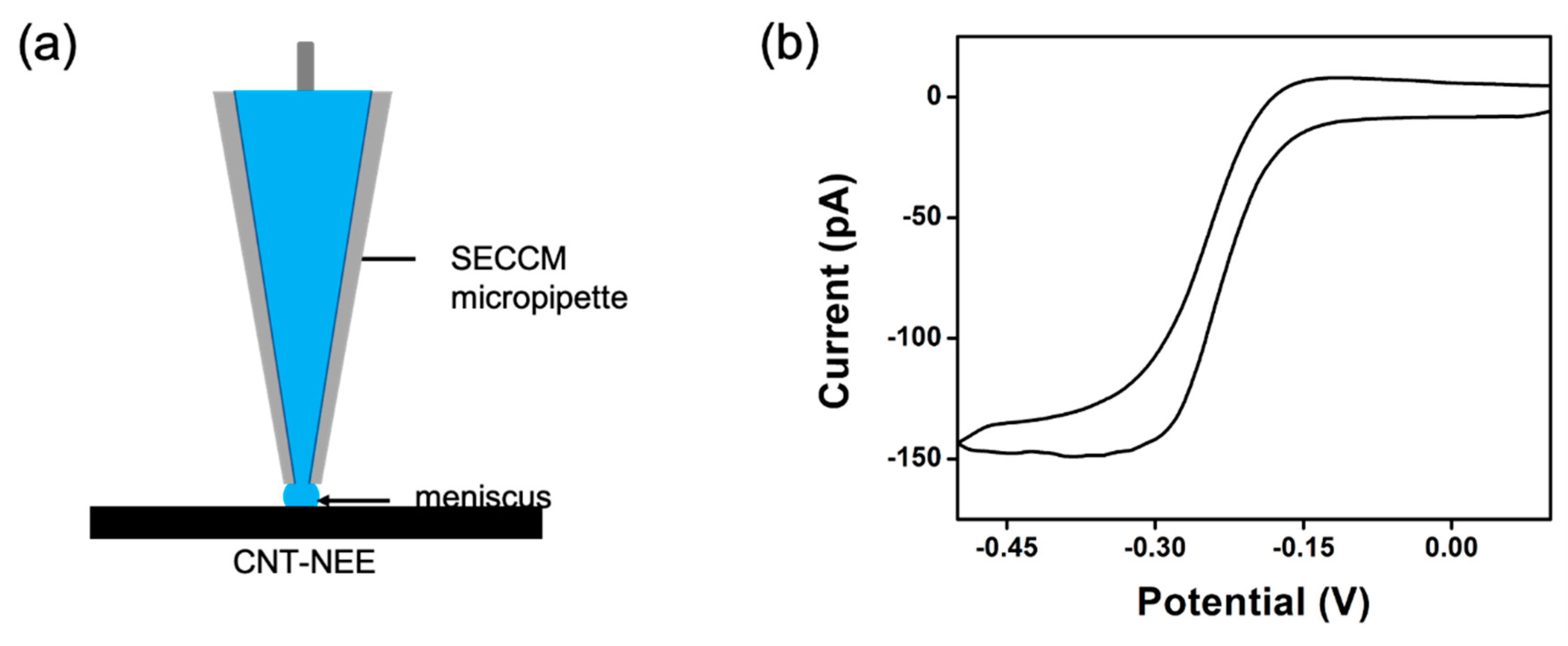
3.3. SECCM Analysis of CNT-NEEs

The SECCM analysis used a CNT-NEE as the working electrode and a quasi-reference counter electrode (QRCE) consisting of a glass capillary with an approximately 200 nm tip containing an Ag/AgCl wire in a solution of 2.5 mM Ruhex and 25 mM KCl. A droplet of the redox solution protruding from the tip of the glass capillary formed a meniscus, which was brought into contact with the CNT-NEE (Figure 7a). Establishment of this connection between the working electrode and QRCE induced the reduction of Ruhex, and the corresponding CV response was collected (Figure 7b). Because the CNT-NEE was fabricated from alternating layers of CNTs and HNBR, the CV response as the SECCM probe was moved across the substrate, indicating whether the analyzed section contained CNTs or only the polymer. As only a small area (~200 nm) of the CNT-NEE was in contact with the meniscus, a steady-state current response was observed (Figure 7b). The main information extracted from SECCM was the homogenous nature of the CNT nanoelectrodes on the surface. By moving across the electrode active area, we were able to evaluate the similarity of the CNT nanoelectrodes distribution in the CNT-NEE. Unless the meniscus was moved to the protecting epoxy surface, the current responses determined by SECCM were quite similar.

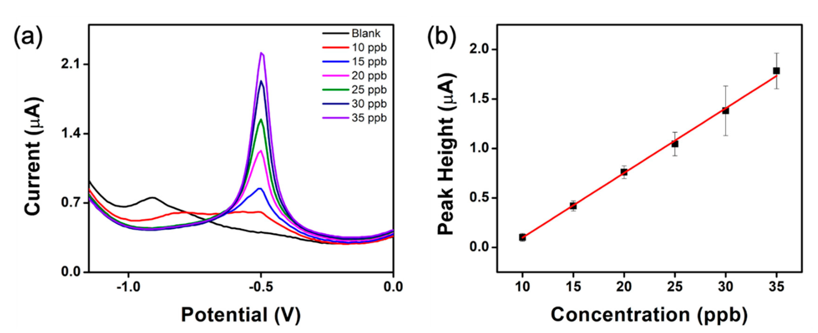
3.4. Lead Detection in Acetate Buffer

The CNT-NEE was applied to the detection of Pb2+ in 0.1 M acetate buffer (pH 4.5, 40 mL) using square-wave anodic stripping voltammetry (SWASV). The deposition potential (Edep) was −2.0 V, and the deposition time (tdep) was 300 s. After the deposition of Pb2+ on the CNT-NEE, it was stripped off in the potential window of −2.0 V to +0.3 V with a potential step (Estep) of 0.010 V, an amplitude of 0.05 V, and a frequency of 30 Hz. The SWASV response of the CNT-NEE increased as the concentration of Pb2+ in acetate buffer (pH 4.5) increased, as shown in Figure 8a, and a linear range of 10–35 ppb Pb2+ was observed. A calibration curve was constructed by plotting the peak height against Pb2+ concentration (Figure 8b).
i p ( μ A ) = ( 0.065 ± 0.001 ) C ( ppb ) ( 0.555 ± 0.017 )
R 2 = 0.999
The limit of detection (LOD) was determined to be 0.57 ppb, using L O D = 3 S a / b , where S a is the standard deviation of the blank solution, and b is the slope of the calibration curve. The relative standard deviation (RSD) for the reproducibility of the CNT-NEE electrodes was 18.3%, while the RSD for repeatability was 14.7%, (see the SI for more information). Controlled potential electrolysis (CPE) was performed as a cleaning method between runs for 120 s at +0.1 V, which has shown to be effective to achieve good reproducibility and repeatability. Previously, Tu et al. reported the detection of Pb2+ in 0.1 M NaNO3 at concentrations as low as 2 ppb Pb2+ using a CNT-NEA modified with a mercury film [4]. Liu et al. used a CNT-NEA coated with a bismuth film to detect heavy metals in 0.1 M acetate buffer (pH 4.5), and an LOD of 40 ppt was achieved for both lead and cadmium [5]. Both mercury and bismuth are known to aid in the detection of lead in solution. In contrast, the CNT-NEE reported here is capable of detecting the World Health Organization maximum contamination level of 10 ppb Pb2+ without using any additional metals.

4. Conclusions

This work demonstrated a simple CNT-NEE fabrication method using drawable CNTs, which limited the nanoelectrode dimensions in at least one direction to a maximum of 50 nm. SEM imaging clearly revealed the random distribution, spacing, and density of the CNT nanoelectrodes. Although the CNT nanoelectrodes were visibly isolated from each other, the CNT-NEE displayed macroelectrode performance for traditional CV measurements using Ru(NH3)63+/2+, which was attributed to overlapping diffusion profiles. However, electrochemical characterization of the CNT-NEE using SECCM revealed true nanoelectrode performance. The observed sigmoidal voltammograms were indicative of a steady state at the interface due to the reduced electrode area in contact with the electroactive solution. Furthermore, the CNT-NEE achieved an LOD of 0.57 ppb for the detection of toxic Pb2+ in acetate buffer, thus demonstrating the potential applicability of the CNT-NEE as an electrochemical sensor.

Supplementary Materials

The following are available online at https://www.mdpi.com/article/10.3390/app11188399/s1, Figure S1: SEM image at 10,000× used to determine percentage of CNTs versus HNBR with in the CNT-NEEs. Red outline around image show total area used, while smaller read lines shows approximate areas where CNTs are exposed. Figure S2: Light microscope image at 100× of the CNT-NEE used to determine the total area of CNTs and HNBR exposed to solution. The red line defines the area. Figure S3: Current density for Glassy carbon, CNT-NEE 1, CNT-NEE 2, and CNT-NEE 3 in 50 mM KCl at 0.01 V/s. Figure S4: Scan rate versus peak current for CNT-NEE. Figure S5: Water window on CNT-NEE in 50 mM KCl. Figure S6: (a) Current vs potential for Glassy carbon, CNT-NEE 1, CNT-NEE 2, and CNT-NEE 3 (b) current density for Glassy carbon, CNT-NEE1, CNT-NEE 2, and CNT-NEE 3 normalized using geometrical areas. Figure S7: (a) Peak heights for 10 ppb Pb2+ determined from one electrode over multiple runs blue line indicates peak height for 15 ppb Pb2+ while red line indicates the baseline from SWASV. (b) Peak heights compared for different CNT-NEE electrodes blue line indicated the peak height for 15 ppb Pb2+ and the red line indicated the baseline from SWASV.

Author Contributions

Conceptualization, N.T.A.; Formal analysis, G.R.D. and N.T.A.; Investigation, G.R.D., H.K. and C.E.R.; Supervision, N.T.A.; Validation, N.T.A.; Writing—original draft, G.R.D.; Writing—review & editing, R.W. and N.T.A. All authors have read and agreed to the published version of the manuscript.

Funding

University of Cincinnati professorship start-up funds for N.T.A.

Institutional Review Board Statement

Not applicable.

Informed Consent Statement

Not applicable.

Conflicts of Interest

The authors declare no conflict of interest.

References

  1. Compton, R.G.; Wildgoose, G.G.; Rees, N.V.; Streeter, I.; Baron, R. Design, fabrication, characterisation and application of nanoelectrode arrays. Chem. Phys. Lett. 2008, 459, 1–17. [Google Scholar] [CrossRef]
  2. Arrigan, D.W.M. Nanoelectrodes, nanoelectrode arrays and their applications. Analyst 2004, 129, 1157–1165. [Google Scholar] [CrossRef] [PubMed]
  3. Tu, Y.; Lin, Y.; Ren, Z.F. Nanoelectrode arrays based on low site density aligned carbon nanotubes. Nano Lett. 2003, 3, 107–109. [Google Scholar] [CrossRef] [Green Version]
  4. Tu, Y.; Lin, Y.; Yantasee, W.; Ren, Z. Carbon nanotubes based nanoelectrode arrays: Fabrication, evaluation, and application in voltammetric analysis. Electroanalysis 2005, 17, 79–84. [Google Scholar] [CrossRef]
  5. Liu, G.; Lin, Y.; Tu, Y.; Ren, Z. Ultrasensitive voltammetric detection of trace heavy metal ions using carbon nanotube nanoelectrode array. Analyst 2005, 130, 1098–1101. [Google Scholar] [CrossRef]
  6. Lin, R.; Lim, T.M.; Tran, T. Enhancement of mass transfer coefficient towards carbon nanotube nanoelectrode array. Sens. Actuators B Chem. 2018, 260, 1052–1058. [Google Scholar] [CrossRef]
  7. Patil, A.V.; Beker, A.F.; Wiertz, F.G.M.; Heering, H.A.; Coslovich, G.; Vlijm, R.; Oosterkamp, T.H. Fabrication and characterization of polymer insulated carbon nanotube modified electrochemical nanoprobes. Nanoscale 2010, 2, 734–738. [Google Scholar] [CrossRef]
  8. Lin, Y.; Lu, F.; Tu, Y.; Ren, Z. Glucose biosensors based on carbon nanotube nanoelectrode ensembles. Nano Lett. 2004, 4, 191–195. [Google Scholar] [CrossRef]
  9. Liu, Y.; Zhang, J.; Cheng, Y.; Jiang, S.P. Effect of Carbon Nanotubes on Direct Electron Transfer and Electrocatalytic Activity of Immobilized Glucose Oxidase. ACS Omega 2018, 3, 667–676. [Google Scholar] [CrossRef] [PubMed]
  10. Menon, V.P.; Martin, C.R. Fabrication and evaluation of nanoelectrode ensembles. Anal. Chem. 1995, 67, 1920–1928. [Google Scholar] [CrossRef]
  11. Karimian, N.; Moretto, L.M.; Ugo, P. Nanobiosensing with arrays and ensembles of nanoelectrodes. Sensors 2017, 17, 65. [Google Scholar] [CrossRef]
  12. Habtamu, H.B.; Sentic, M.; Silvestrini, M.; De Leo, L.; Not, T.; Arbault, S.; Manojlovic, D.; Sojic, N.; Ugo, P. A sensitive electrochemiluminescence immunosensor for celiac disease diagnosis based on nanoelectrode ensembles. Anal. Chem. 2015, 87, 12080–12087. [Google Scholar] [CrossRef]
  13. Gaetani, C.; Ambrosi, E.; Ugo, P.; Moretto, L.M. Electrochemical immunosensor for detection of IgY in food and food supplements. Chemosensors 2017, 5, 10. [Google Scholar] [CrossRef] [Green Version]
  14. Kim, D.S.; Kang, E.S.; Baek, S.; Choo, S.S.; Chung, Y.H.; Lee, D.; Min, J.; Kim, T.H. Electrochemical detection of dopamine using periodic cylindrical gold nanoelectrode arrays. Sci. Rep. 2018, 8, 14049. [Google Scholar] [CrossRef] [PubMed] [Green Version]
  15. Kim, T.H.; Yea, C.H.; Chueng, S.T.D.; Yin, P.T.T.; Conley, B.; Dardir, K.; Pak, Y.; Jung, G.Y.; Choi, J.W.; Lee, K.B. Large-scale nanoelectrode arrays to monitor the dopaminergic differentiation of human neural stem cells. Adv. Mater. 2015, 27, 6356–6362. [Google Scholar] [CrossRef] [PubMed]
  16. Li, Z.; Liu, C.; Sarpong, V.; Gu, Z. Multisegment nanowire/nanoparticle hybrid arrays as electrochemical biosensors for simultaneous detection of antibiotics. Biosens. Bioelectron. 2019, 126, 632–639. [Google Scholar] [CrossRef]
  17. Habtamu, H.B.; Ugo, P. Miniaturized enzymatic biosensor via biofunctionalization of the insulator of nanoelectrode ensembles. Electroanalysis 2015, 27, 2187–2193. [Google Scholar] [CrossRef]
  18. Beluomini, M.A.; Karimian, N.; Stradiotto, N.R.; Ugo, P. Tailor-made 3d-nanoelectrode ensembles modified with molecularly imprinted poly(o-phenylenediamine) for the sensitive detection of L-arabitol. Sens. Actuators B Chem. 2019, 284, 250–257. [Google Scholar] [CrossRef]
  19. Li, R.; Cao, L.; Liang, C.; Sun, S.; Liu, H.; Yan, P. Development and modeling of an ultrasensitive label-free electrochemical immunosensor for okadaic acid based on polythionine-modified three-dimensional gold nanoelectrode ensembles. Ionics 2020, 26, 4661–4670. [Google Scholar] [CrossRef]
  20. Ongaro, M.; Mardegan, A.; Stortini, A.M.; Signoretto, M.; Ugo, P. Arrays of templated TiO2 nanofibres as improved photoanodes for water splitting under visible light. Nanotechnology 2015, 26, 165402. [Google Scholar] [CrossRef]
  21. Ongaro, M.; Signoretto, M.; Trevisan, V.; Stortini, A.M.; Ugo, P. Arrays of TiO2 nanowires as photoelectrochemical sensors for hydrazine detection. Chemosensors 2015, 3, 146–156. [Google Scholar] [CrossRef] [Green Version]
  22. Shanmugam, N.R.; Muthukumar, S.; Chaudhry, S.; Anguiano, J.; Prasad, S. Ultrasensitive nanostructure sensor arrays on flexible substrates for multiplexed and simultaneous electrochemical detection of a panel of cardiac biomarkers. Biosens. Bioelectron. 2017, 89, 764–772. [Google Scholar] [CrossRef]
  23. Wang, H.H.; Chen, X.J.; Li, W.T.; Zhou, W.H.; Guo, X.C.; Kang, W.Y.; Kou, D.X.; Zhou, Z.J.; Meng, Y.N.; Tian, Q.W.; et al. ZnO nanotubes supported molecularly imprinted polymers arrays as sensing materials for electrochemical detection of dopamine. Talanta 2018, 176, 573–581. [Google Scholar] [CrossRef]
  24. Luo, J.; Wan, M.; Cui, J.; Zhang, X.; Zhang, Y.; Wang, Y.; Qin, Y.; Zheng, H.; Wu, Y. Synthesis of nonstoichiometric CeO2@CNT core/shell nanowire arrays and their applications in biosensing. Mater. Lett. 2017, 188, 275–279. [Google Scholar] [CrossRef]
  25. Jamal, M.; Hasan, M.; Mathewson, A.; Razeeb, K.M. Disposable sensor based on enzyme-free ni nanowire array electrode to detect glutamate. Biosens. Bioelectron. 2013, 40, 213–218. [Google Scholar] [CrossRef]
  26. Dincer, C.; Ktaich, R.; Laubender, E.; Hees, J.J.; Kieninger, J.; Nebel, C.E.; Heinze, J.; Urban, G.A. Nanocrystalline boron-doped diamond nanoelectrode arrays for ultrasensitive dopamine detection. Electrochim. Acta 2015, 185, 101–106. [Google Scholar] [CrossRef]
  27. Periyakaruppan, A.; Gandhiraman, R.P.; Meyyappan, M.; Koehne, J.E. Label-free detection of cardiac troponin-I using carbon nanofiber based nanoelectrode arrays. Anal. Chem. 2013, 85, 3858–3863. [Google Scholar] [CrossRef] [Green Version]
  28. Koehne, J.E.; Marsh, M.; Boakye, A.; Douglas, B.; Kim, I.Y.; Chang, S.Y.; Jang, D.P.; Bennet, K.E.; Kimble, C.; Andrews, R.; et al. Carbon nanofiber electrode array for electrochemical detection of dopamine using fast scan cyclic voltammetry. Analyst 2011, 136, 1802–1805. [Google Scholar] [CrossRef] [Green Version]
  29. Abbott, J.; Ye, T.; Qin, L.; Jorgolli, M.; Gertner, R.S.; Ham, D.; Park, H. CMOS nanoelectrode array for all-electrical intracellular electrophysiological imaging. Nat. Nanotechnol. 2017, 12, 460–466. [Google Scholar] [CrossRef]
  30. Jeoung, E.; Galow, T.H.; Schotter, J.; Bal, M.; Ursache, A.; Tuominen, M.T.; Stafford, C.M.; Russell, T.P.; Rotello, V.M. Fabrication and characterization of nanoelectrode arrays formed via block copolymer self-assembly. Langmuir 2001, 17, 6396–6398. [Google Scholar] [CrossRef]
  31. Chen, Y.; Hsu, J.; Chen, Z.; Lin, Y.; Hsu, Y. Fabrication of Fe3O4 nanotube arrays for high-performance non-enzymatic detection of glucose. J. Electroanal. Chem. 2017, 788, 144–149. [Google Scholar] [CrossRef]
  32. Abbott, J.; Ye, T.; Ham, D.; Park, H. Optimizing nanoelectrode arrays for scalable intracellular electrophysiology. Acc. Chem. Res. 2018, 51, 600–608. [Google Scholar] [CrossRef] [PubMed]
  33. Ongaro, M.; Ugo, P. Bioelectroanalysis with nanoelectrode ensembles and arrays. Anal. Bioanal. Chem. 2012, 405, 3715–3729. [Google Scholar] [CrossRef]
  34. Koehne, J.E.; Li, J.; Cassell, A.M.; Chen, H.; Ye, Q.; Han, J.; Meyyappan, M. System optimization for the development of ultrasensitive electronic biosensors using carbon nanotube nanoelectrode arrays. Mech. Chem. Biosyst. 2004, 1, 69–80. [Google Scholar] [CrossRef] [PubMed]
  35. Ye, J.S.; Bai, Y.C.; Zhang, W.D. Modification of vertically aligned carbon nanotube arrays with palladium nanoparticles for electrocatalytic reduction of oxygen. Microchim. Acta 2009, 165, 361–366. [Google Scholar] [CrossRef]
  36. Yun, Y.H.; Dong, Z.; Shanov, V.N.; Doepke, A.; Heineman, W.R.; Halsall, H.B.; Bhattacharya, A.; Wong, D.K.Y.; Schulz, M.J. Fabrication and characterization of carbon nanotube array electrodes with gold nanoparticle tips. Sens. Actuators B Chem. 2008, 133, 208–212. [Google Scholar] [CrossRef]
  37. Lin, R.; Lim, T.M.; Tran, T. Carbon nanotube band electrodes for electrochemical sensors. Electrochem. Commun. 2018, 86, 135–139. [Google Scholar] [CrossRef]
  38. Wang, Z.; Latonen, R.M.; Kvarnström, C.; Ivaska, A.; Niu, L. Preparation of multi-walled carbon nanotube/amino-terminated ionic liquid arrays and their electrocatalysis towards oxygen reduction. Materials 2010, 3, 672–681. [Google Scholar] [CrossRef] [Green Version]
  39. Koehne, J.; Chen, H.; Li, J.; Cassell, A.M.; Ye, Q.; Ng, H.T.; Han, J.; Meyyappan, M. Ultrasensitive label-free DNA analysis using an electronic chip based on carbon nanotube nanoelectrode arrays. Nanotechnology 2003, 14, 1239–1245. [Google Scholar] [CrossRef]
  40. Koehne, J.; Li, J.; Cassell, A.M.; Chen, H.; Ye, Q.; Ng, H.T.; Han, J.; Meyyappan, M. The fabrication and electrochemical characterization of carbon nanotube nanoelectrode arrays. J. Mater. Chem. 2004, 14, 676–684. [Google Scholar] [CrossRef]
  41. Li, J.; Ng, H.T.; Cassell, A.; Fan, W.; Chen, H.; Ye, Q.; Koehne, J.; Han, J.; Meyyappan, M. Carbon nanotube nanoelectrode array for ultrasensitive DNA detection. Nano Lett. 2003, 3, 597–602. [Google Scholar] [CrossRef]
  42. Koehne, J.E.; Chen, H.; Cassell, A.M.; Ye, Q.; Han, J.; Meyyappan, M.; Li, J. Miniaturized multiplex label-free electronic chip for rapid nucleic acid analysis based on carbon nanotube nanoelectrode arrays. Clin. Chem. 2004, 50, 1886–1893. [Google Scholar] [CrossRef] [PubMed]
  43. Li, J.; Koehne, J.E.; Cassell, A.M.; Chen, H.; Ng, H.T.; Ye, Q.; Fan, W.; Han, J.; Meyyappan, M. Inlaid multi-walled carbon nanotube nanoelectrode arrays for electroanalysis. Electroanalysis 2005, 17, 15–27. [Google Scholar] [CrossRef]
  44. Gupta, P.; Lazenby, R.A.; Rahm, C.E.; Heineman, W.R.; Buschbeck, E.; White, R.J.; Alvarez, N.T. Electrochemistry of controlled diameter carbon nanotube fibers at the cross section and sidewall. ACS Appl. Energy Mater. 2019, 2, 8757–8766. [Google Scholar] [CrossRef]
  45. Alvarez, N.T.; Miller, P.; Haase, M.R.; Lobo, R.; Malik, R.; Shanov, V. Tailoring physical properties of carbon nanotube threads during assembly. Carbon 2019, 144, 55–62. [Google Scholar] [CrossRef]
  46. Alvarez, N.T.; Miller, P.; Haase, M.; Kienzle, N.; Zhang, L.; Schulz, M.J.; Shanov, V. Carbon nanotube assembly at near-industrial natural-fiber spinning rates. Carbon 2015, 86, 350–357. [Google Scholar] [CrossRef]
  47. Yu, Q.; Alvarez, N.T.; Miller, P.; Malik, R.; Haase, M.R.; Schulz, M.; Shanov, V.; Zhu, X. Mechanical strength improvements of carbon nanotube threads through epoxy cross-linking. Materials 2016, 9, 68. [Google Scholar] [CrossRef] [Green Version]
  48. Alvarez, N.T.; Ochmann, T.; Kienzle, N.; Ruff, B.; Haase, M.R.; Hopkins, T.; Pixley, S.; Mast, D.; Schulz, M.J.; Shanov, V. Polymer Coating of carbon nanotube fibers for electric microcables. Nanomaterials 2014, 4, 879–893. [Google Scholar] [CrossRef]
  49. Gazica, K.; FitzGerald, E.; Dangel, G.; Haynes, E.N.; Yadav, J.; Alvarez, N.T. Towards on-site detection of cadmium in human urine. J. Electroanal. Chem. 2020, 859, 113808. [Google Scholar] [CrossRef]
  50. Ferrari, A.G.M.; Foster, C.W.; Kelly, P.J.; Brownson, D.A.C.; Banks, C.E. Determination of the electrochemical area of screen-printed electrochemical sensing platforms. Biosensors 2018, 8, 53. [Google Scholar] [CrossRef] [Green Version]
Figure 1. Illustration of the CNT-NEE fabrication process. (a) Ribbon-like CNTs drawn by a moving belt onto a Teflon substrate, where liquid HNBR is sprayed onto the CNT ribbon. (b) Photograph of the ribbon-like CNTs employed for CNT-NEE fabrication.
Applsci 11 08399 g001
Figure 2. SEM images of drawable CNTs assembled into ribbon-like porous structures at magnifications of (a) 650× and (b) 20k×.
Applsci 11 08399 g002
Figure 3. Illustration of the CNT-NEE assembly. (a) Cross-sectional view of the fabricated CNT-NEE. (b) Top view of the CNT-NEE with a higher magnification illustration of the layering of CNTs and HNBR.
Applsci 11 08399 g003
Figure 4. SEM images of the CNT-NEE: (a) untreated thin film after microtoming and (b) film after plasma treatment for 60 s at 1000× magnification.
Applsci 11 08399 g004
Figure 5. CNT-NEE characterization. (a) Optical microscope image of the electrode face at 150× magnification. The exposed area of the CNT-NEE is outlined in red. (b) Cyclic voltammograms of the GC electrode (black) and CNT-NEE 1 (red), CNT-NEE 2 (blue), and CNT-NEE 3 (pink) in 2.5 mM Ruhex and 25 mM KCl at a scan rate of 0.01 V/s normalized by the active area of each electrode.
Applsci 11 08399 g005
Figure 6. Scan rate study of the CNT-NEE. (a) Cyclic voltammograms collected at scan rates of 0.001, 0.005, 0.01, 0.02, 0.05, 0.08, 0.1, 0.125, 0.15, and 0.2 V/s in 2.5 mM Ruhex and 25 mM KCl. (b) ip vs. υ 1 / 2 plots (black squares: ipc; red circles: ipa) for the CNT-NEE (n = 3).
Applsci 11 08399 g006
Figure 7. SECCM characterization of the CNT-NEE. (a) Illustration of the SECCM contact area, where the CNT-NEE is the working electrode and an Ag/AgCl wire inserted in the micropipette is the QRCE. (b) Sigmoidal voltammogram collected using SECCM.
Applsci 11 08399 g007
Figure 8. Lead detection using the CNT-NEE. (a) SWASV response in 0.1 M acetate buffer (pH 4.5) with varying concentrations Pb2+ (0, 10, 15, 20, 25, 30, and 35 ppb). (b) Calibration curve for Pb2+ detection (n = 3).
Applsci 11 08399 g008
Table 1. Characteristics of CNT-NEEs and the glassy carbon electrode.
Cathodic Peak Current (µA)Anodic Peak Current (µA)Active Area (cm2) from ipcGeometrical Area (cm2)
CNT-NEE 11.59−1.420.01010.0084
CNT-NEE 21.62−1.410.00510.0120
CNT-NEE 31.70−1.410.00620.0082
Glassy Carbon14.9−12.90.14930.0706
Publisher’s Note: MDPI stays neutral with regard to jurisdictional claims in published maps and institutional affiliations.

